Note: Descriptions are shown in the official language in which they were submitted.
- ~2&37~
" . 1
1 TITLE OF THE INVENTION
PHOTONIC SWITC~ING SYSTEM
BACKGROUND OF THE INVENTION
The present invention generally relates to
photonic switching systems, and more particularly to a
photonic switching system which cross connects, drops or
inserts optical signal links of a plurality of channels.
In a broadband integrated services digital
lo network (ISDN), it is necessary to use a transmission
apparatus having a throughput in the order of 42.3
Gbps. In other words, it must be possible to cross
connect, drop or insert 155.520 Mbps data of
approximately 272 channels.
In a conventional system which cross connects,
drops or inserts optical signal links of a plurality of
channels, the process of cross connecting, dropping or
inserting is carried out after once converting a
received optical signal into an electrical signal, and
the processed electrical signal is converted back into
an optical signal before being transmitted to a
terminal, a subscriber or a next node.
When carrying out the process electrically, it
is necessary to use a large scale integrated circuit
(LSI) having a high performance and capable of
processing a large number of signals which are
transmitted at a high transmission rate, but the
performance of the existing LSI cannot meet such a
demand. Even if an LSI having such a high performance
were existed, the number of input and output pins would
become extremely large, it would be extremely
troublesome to equip the system with such an LSI, and
required coaxial cables and interconnections would
become extremely complex and large in scale. For this
reason, there is a problem in that it is extremely
difficult to realize by the conventional method a
switching system whicn -s capable of swi.chlns cptical
-" 2~ 78 : ~
2 27879-47E
signal links as the signal capacity further increases in the
; future.
SUMMARY OF THE I~VENTION
Accordingly, it is a general object of the present
invention to provide a novel and use$ul photonic switching system
in which the problems de~cribed above are eliminated.
Another and more specific object of the present
invention is to provide a photonic switching system comprising:
an optical link conversion board having a first end and a second
end opposite to the first end; a plurallty of variable wavelength
light emitting elements arranged at a constant pitch along the
first end of said optical link conversion board and emitting
optical signal components having different wavelengths; a single
optical star coupler means mixing the optical signal components
received from said light emitting elements and outputting a mixed
optical slgnal; and a plurality of multi-wavelength selective
fllters arranged at a constant pitch along the second end of said
optical link conversion board and receiving and processing only
the mixed optical signal from said single optical star coupler
means, each of said multi-wavelength selective filters selectively
outputting an optical signal which includes optical signal
components having desired wavelengths out of the wavelengths
included in the optical signal components making up the mixed
optical signal.
Still another ob~ect of the present invention is to
provide a photonic switching system comprising: an optical llnk
converslon board havlng a first end and a second end opposite to
the flrst end; a plurality of variable wavelength llght emitting
212~78
3 27879-47E
elements arranged at a constant pitch along the first end of said
optical link conversion board and emitting op~ical signal
components having different wavelengths; optical star coupler
means mixing ~he optical signal components received from said
light emitting elements and outputting a mixed optical signal; and
a plurality of multi-wavelength selective filters arranged at a
constant pitch along the second end of said optical link
conversion board and receiving the mixed optical signal from said
optical star coupler means, each of said multi-wavelength
selective filters selectively outputting an optical ~ignal which
includes optical signal components having desired wavelengths out
of the wavelengths included in the optical signal components
making up the mixed optical signal, wherein said multi-wavelength
selective filter comprises a first optical star coupler ~hich
drops the mixed optlcal signal received from said optical star
coupler means and outputs optical signals, a plurality of
wavelength selecting elements which receive the optical signals
from aid first optical star coupler and respectively output
optical signal component~ from said wavelength selecting elements
and outputs the optical signal which includes the optical signal
components having the desired wavelengths.
Other objects and further features of the present
invention will be apparent from the following detailed description
when read in con~unctlon with the accompanying drawings.
BRIEF DESCRIPTION OF THE DRAWINGS
Figure 1 is a system block diagram generally showing an
optical link conversion board of a conceivable photonic switching
system;
~2S~
4 27879-47E
Figure 2 i5 a perspective view ~howing the conceivable
photonic switching system;
Figure 3 is a system block diagram generally showing an
optical link conversion board of another conceivable photonlc
switching system;
Figure 4 is a system block diagram showing an optical
link conversion board of a first embodiment of a photonic
switching system accordlng to the present lnvention;
Flgure 5 is a system block diagram showing an optical
link converslon board of a second embodiment of the photonic
switchlng system accordlng to the present lnventlon;
Figures 6 and 7 are system block diagrams for explaining ;
the blocking which occurs depending on the number of stages of
optical link converslon board groups;
Figures 8 and 9 are system block diagram~ respectlvely
showing optical link conversion boards of first and second optical
link conversion board groups used in a third embodiment of the
photonic switching system according to the present invention;
Figure 10 i5 a perspective view generally showing the
third embodiment of the photonlc switching system
212~7~
-- 5
1 according to the present invention;
FIG.ll is a system block diagram showing an
embodiment of a multi-wavelength selective filter;
FIG.12 is a system block diagram generally
showing an optical link conversion board of a first
optical link conversion board group used in a fourth
embodiment of the photonic switching system according to
the present invention;
FIGS.13A through 13C are diagrams for
explaining the fourth embodiment of the photonic
switching system;
FIG.14 is a system block diagram for
explaining another embodiment of a multi-wavelength
selective filter;
FIG.15 is a system block diagram showing the
multi-wavelength selective filter shown in FIG.14 in
more detail; and
FIG.16 shows an embodiment of a fiber notch
filter shown in FIG.15.
DESCRIPTION OF THE PREFERRED EMBODIMENTS
First, a description will be given of a
conceivable photonic switching system so as to
facilitate the understanding of the present invention.
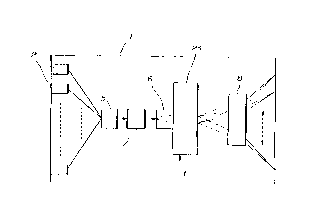
FIG.l shows an optical link conversion board l
of the conceivable photonic switching system. The
optical link conversion board 1 is made of a light guide
material and has a generally flat shape.
A plurality of wavelength converter elements 2
which can convert the wavelength of input light
(hereinafter referred to as an optical signal) into
arbitrary wavelength are provided on the left end of the
optical link conversion board l in FIG.l at a constant
pitch. Each wavelength converter element 2 has a light
3S input end facing left and a light output end facing
right in FIG.l. For example, 16 or 17 wavelength
converter elements 2 are provided. For example, a
: ,,
2~2~78
- 6 -
1 wavelength converting laser diode which can freely
convert the wavelength of the input optical signal by
controlling an applying current may be used for the
wavelength converter element 2.
A combiner 5 combines output optical signals
of all the wavelength converter elements 2 and outputs
an optical signal to a deflector 3. For example, a
photocoupler is used as the combiner 5. The combiner 5
is provided at a central part of the optical link
conversion board 1, and output ends of the wavelength
converter elements 2 and the combiner 5 are optically
coupled via guide means 9 such as optical waveguides and
optical fibers.
In principle, the deflector 3 may use
refraction of a prism. The deflector 3 deflects the
optical signal from the combiner 5 in different
directions depending on the wavelength, and optical
signals are output from the right end of the optical
link conversion board 1 at a constant interval.
Accordingly, the optical signals input to the
wavelength converter elements 2 at the left end of the
light link conversion board 1 are output from different
positions at the right end of the optical link
conversion board 1 depending on the wavelength converted
in each wavelength converter element 2.
In other words, by controlling the wavelength
at each wavelength converter element 2, each optical
signal is output from an arbitrary position at the right
end of the optical link conversion board 1.
As shown in FIG.2, a plurality of the above
described optical link conversion boards 1 are arranged
in parallel to form an optical link conversion board
group. For example, a first optical link conversion
board group la is made up of 16 optical link conversion
boards 1 which are arranged vertically and are mutually
parallel. For example, a second optical link conversion
board group lb is made up of 17 optical link conversion
~ .
-' 2}2~7~
1 boards 1 which are arranged horizontally and are
mutually parallel. For example, a third optical link
conversion board group lc is made up of 16 optical link
conversion boards 1 which are arranged vertically and
are mutually parallel.
Each light input end (wavelength converter
element 2) of the first optical link conversion board
group la is arranged to match a corresponding one of
light output positions of 16 (horizontal) x 17
tvertical) = 272 channels of an optical transmitter part
101. In addition, the first and second optical link
conversion board groups la and lb are coupled in series
and perpendicular to each other so that each light
output position of the first optical link conversion
board group la matches a corresponding one of light
input ends (wavelength converter elements 2) o~ the
second optical link conversion ~oard group lb.
Similarly, the second and third optical link
conversion board groups lb and lc are coupled in series
and perpendicular to each other so that each light
output position of the second optical link conversion
board group lb matches a corresponding one of light
input ends (wavelength converter elements 2) of the
third optical link conversion board group lc. In this
case, each optical link conversion board l of the first
and third optical link conversion board groups la and lc
has 17 wavelength converter elements 2, and each optical
link conversion board 1 of the second optical link
conversion board group lb has 16 wavelength converter
elements 2.
According to this conceivable photonic
switching system, the wavelength of the output optical
signal may be adjusted individually in each of the first
through third optical link conversion board groups la
through lc so as to guide the optical signal output from
each optical communication channel of the optical
transmitter part 101 to an arbitrary optical
212~878
1 communication channel of an optical receiver part 102.
Of course, it is possible to arrange the first
and third optical link conversion board groups la and lc
horizontally and the second optical link conversion
board group lb vertically with respect to the optical
transmitter part 101 and the optical receiver part 102.
If blocking is permitted, it is possible to
omit the third optical link conversion board group lc
and form the photonic switching system using only two
stages of optical link conversion board groups (that is,
the first and second optical link conversion board
groups la and lb). However, when three stages of
optical link conversion board groups are provided as
shown in FIG.2, it becomes possible to carry out a
blocking-free routing of optical signals.
FIG.3 shows an optical link conversion board
of another conceivable photonic switching system. In
FIG.3, those parts which are the same as those
corresponding parts in FIGS.l and 2 are designated by
the same reference numerals, and a description thereof
will be omitted.
In the optical link conversion board la shown
in FIG.3, a variable wavelength light emitting element 4
which can emit an optical signal having an arbitrary
wavelength is provided in place of the wavelength
con~erter element 2. In addition, the optical link
conversion board 1 of tha first optical link conversion
board group la and the optical transmitter part 101 may
be provided integrally. For example, a wavelength
tunable laser diode which generates laser beams of
different wavelengths by varying the applying current
may be used for the variable wavelength light emitting
element 4.
Next, a description will be given of a first
embodiment of a photonic switching system according to
the present invention, by referring to FIG.4. In FIG.4,
those parts which are the same as those corresponding
212& ?178
-~ _ 9 _
1 parts in FIGS.l and 3 are designated by the same
reference numerals, and a description thereof will be
omitted.
The optical link conversion board l shown in
FIG.4 may be used as each of the first through third
optical link conversion groups la through lc shown in
FIG.3. In FIG.4, a photocoupler 5 is used as the
combiner and an acousto-optic device 23 is used as the
deflector. A collimator 6 forms the output light of the
photocoupler 5 into parallel light beams, and an optical
amplifier 7 compensates for the optical loss at the
acousto-optic device 23. A lens 8 converges the light
beam at the light output position.
A signal having an RF frequency f is applied
to the acousto-optic device 23. An angle e of
diffraction of the acousto-optic device 23 can be
described by ~ = f~/v, where ~ denotes the wavelength
and v denotes the speed of sound within an acousto-optic
medium.
Accordingly, in order to change ~, the RF
frequency f or the speed v is changed. When an optical
signal including optical signal components having
various wavelengths is input to the acousto-optic device
23, the input optical signal (light) takes an angle of
diffraction dependent~-on the wavelength and is deflected
in different directions without the need to change the
RF frequency f. Hence, by appropriately selecting the
RF frequency f, the optical signal components having
different wavelengths can be ouL~L sequentially from
the right end of the optical link conversion board 1 at
constant intervals depending on the wavelength.
FIG.5 shows an optical link conversion board
of a second embodiment of the photonic switching system
according to the present invention. In FIG.5, those
parts which are the same as those corresponding parts in
FIGS.3 and 4 are designated by the same reference -
numerals, and a description thereof will be omitted.
212~87~
-- 10 --
1 In this embodiment, the variable wavelength
- light emitting element 4 is provided in place of the
wavelength converter element 2 of the optical link
conversion board 1 of the first optical link conversion
board group la.
In addition, it is possible to deflect the
optical signal to a predetermined light output position
by inputting the input optical signal to dif~erent
acousto-optic devices 23 and applying signals having
different RF frequencies f to the acousto-optic devices
23.
Furthermore, it is possible to use a
; diffraction grating or a hologram as the beam
deflector. A wave length divider may be used in place
of the acousto-optic device 23 and the optical signal
may be guided thereafter to the predetermined light
output position using an optical fiber or the like.
Moreover, a light refractive index crystal may
be used in place of the acousto-optic device 23. In
this case, a diffraction grating is formed by
irradiating on the crystal light beams from both sides
with an angle of 45~ in both the upward and downward
directions.
However, in the first and second embodiments
described above, it is~impossible to freely guide the
optical signals from all input positions to any output
position when only two stages of the optical link
conversion board groups are used, and the so-called
blocking occurs. For this reason, it is necessary to
connect three stages of the optical link conversion
board groups in order to carry out the blocking-free
routing of the optical signals.
FIG.6 shows a case where only two stages of
optical link conversion board groups are connected,
where there are 3 x 3 = 9 input ports and output ports.
When the input signals at the input ports 3 and b
respectively are to be output from the output ports G
212~378
1 and H, it is only possible to output the signal at the
input port a to the output port G or the signal at the
input port b to the output port G because there is only
one route which connects optical link conversion boards
301 and 302 as indicated by a thick solid line in
FIG.6. In other words, the blocking occurs.
On the other hand, FIG.7 shows a case where
three stages of optical link conversion board groups are
connected, where there are 3 x 3 = 9 input ports and
output ports. When the input signals at the input ports
a and b respectively are to be output from the output
ports G and H, it is possible to output the signal at
the input port a to the output port G and to output the
signal at the input port b to the output port G because
there are more than one route connecting optical link
conversion boards 201 and 202 as indicated by a thick
solid line in FIG.7. In FIG.7, there are three routes
connecting the optical link conversion boards 201 and
202, and no blocking occurs.
Next, a description will be given of
embodiments in which the blocking can be prevented even
when only two stages of optical link conversion board
groups are connected.
FIGS.8 and 9 are system block diagrams ;~
respectively showing optical link conversion boards of
in first and second optical link conversion board groups
which are used in a third embodiment of the photonic
switching system according to the present invention. In
FIGS.8 and 9, those parts which are the same as those
corresponding parts in FIGS.4 and 5 are designated by
the same reference numerals, and a description thereof
will be omitted.
In FIG.8, an optical link conversion board 11
which forms a first optical link conversion board group
lla has the variable wavelength light emitting elements
4 provided at the input (left) end thereof for
generating optical signals having arbitrary
. ~
~ .
.
.
212~87~
- 12 -
1 wavelengths. An optical star coupler 15 is provided at
the central part of the optical link conversion board 11
for mixing the optical signals output from all of the
variable wavelength light emitting elements 4. The
mixed optical signal is guided to the light output
positions at the output (right) end. A multi-wavelength
selective filter 13 is provided at each light output
position. The multi-wavelength selective filter 13
selects an arbitrary wavelength out of the mixed optical
signal. Hence, from each light output position, it is
possible to output an arbitrary number of optical signal
components having arbitrary wavelengths or to output no
optical signal. The optical link conversion board 11 of
the first optical link conversion board group lla and
the optical transmitter part 101 mayr or may not be
provided integrally.
In FIG.9, an optical link conversion board 12
which forms a second optical link conversion board group
12a has light input parts 16 provided at the input
(left) end thereof solely for receiving input optical
signal. ~he light input parts 16 are arranged at a
constant pitch. Wavelength filters 17 are provided at
the output (right) end of the optical link conversion
board 12 The wavelength filters 17 are arranged at a
constant pitch. Each wavelength filter 17 selectively
outputs an optical signal component having an arbitrary
wavelength out of the optical signal received from the
optical star coupler 15.
Because the optical link conversion board 11
of the first optical link conversion board group lla has
the structure shown in FIG.8 and the optical link
conversion board 12 of the second optical link
conversion board group 12a has the structure shown in
FIG.9, the plurality of optical signal components output
from one light output position of the optical link
conversion board 11 can be separated and output from
differen~ light output positions of the optical link
'"' '': :
212~78
- 13 -
.
1 conversion board 12. Hence, whPn the first and second
optical link conversion board groups lla and 12a are
connected as shown in FIG.10, it is possible to carry
out the routing of the optical signals from the optical
transmitter part 101 to the optical receiver part 102
without introducing the blocking, although only two
stages of optical link conversion board groups are
provided.
FIG.11 shows an embodiment of the multi-
wavelength selective filter 13. The multi-wavelength
selective filter 13 includes optical star couplers 13a
and 13c and wavelength filters 13b. The optical star
coupler 13a drops the input optical signal into a
plurality of optical signal components. The dropped
optical signal components from the optical star coupler
13a are passed through the wavelength filters 13b. Each
wavelength filter 13b can selectively output optical
signal component having an arbitrary wavelength
dependent on a control signal CNT applied thereto. The
optical signal components from the wavelength filters
13b are mixed and output from the optical star coupler -
13c.
For example, the number of wavelength filters
13b is equal to the number of wavelengths of the optical -
signal components included in the input optical signal.
Hence, it is possible to pass an arbitrary number of
optical signal components having arbitrary wavelengths
by independently controlling the wavelength filters 13b
so that optical signal components having different
wavelengths are permitted to pass or not permitted to
pass at all.
FIG.12 shows the optical link conversion board
11 of the first optical link conversion board group lla
which is used in a fourth embodiment of the photonic
switching system according to the present invention. In
FIG.12, those parts which are the same as those
corresponding parts in FI&S.4 and 8 2r2 design2,ed bv
212~878
- 14 -
1 the same reference numerals, and a description thereof
will be omitted.
In this embcdiment, an acousto-optic device 23
is used in place of the multi-wavelength selective
filter 13. In addition, the acousto-optic device 23 is
driven by a modulation frequency f in which frequencies
fl, f2, ..., fl7 may be multiplexed. The optical star
coupler 15, the collimator 6, the optical amplifier 7
and the lens 8 are the same as those described in
10 conjunction with FIG.4. -
According to this emhodiment, the second
optical link conversion board group 12a may be made up
of the optical link conversion board 12 shown in FIG.9.
By using the second optical link conversion board group
12a and the first optical link conversion board group
lla which is made up of the optical link conversion
board 11 shown in FIG.12, it is also possible to carry
out a blocking-free routing of optical signals using
only two stages of optical link conversion board groups.
In this embodiment, the acousto-optic device
23 deflects one or a plurality of optical signal
components having a plurality of wavelengths to a
desired light output position of the optical link
conversion board 1. FIG.13A shows a case where the RF
frequency f = fl is applied to the acousto-optic -~-
device 23 to deflect the optical signal component having
the wavelength Al to a light output position LOP2.
Similarly, FIG.13B shows a case where the RF frequency f
= f2 is applied to the acousto-optic device 23 to
deflect the optical signal component having the
wavelength A2 to the light output position LOP2.
FIG.13C shows a case where the RF frequency f = f
f2 is applied to the acousto-optic device 23 to
deflect the optical signal components having the
wavelengths ~1 and 12 to the light ~uL~uL position
LOP2.
Hence, according to this embodiment, it is
212~78
- 15 -
1 possible to output to one light output position of the
optical link conversion board 1 an optical signal whicA
includes a plurality of optical signal components having
different wavelengths. This is the reason why it
becomes possible to carry out a blocking-free routing of
optical signals by use of only two stages of optical
link conversion boards.
Of course, the embodiment shown in FIG.4 may
be modified similarly like the fourth embodiment of the
photonic switching system.
In the embodiments described above, the
optical link conversion boards need not be connected
directly, and optical fibers or optical fiber bundles
may be used to connect the optical link conversion
boards. In addition, when a semiconductor laser diode
amplifier or an Er doped fiber having optical amplifying
function is inserted in the optical fibers or optical
fiber bundles, it is possible to compensate for the
optical loss introduced at each optical link conversion
board and prevent characteristic deterioration of the
light receiving circuit on the reception side.
Furthermore, in the described embodiments, the
so-called cross connection is taken as an example of the
optical switching. However, when a part of the input or
output channel is dropped, it is of course possible to
easily carry out the so-called insert or drop.
Next, a description will be given of another
embodiment of tne multi-wavelength selective filter.
According to this embodiment of the multi-wavelength
selective filter, it is possible to extract an arbitrary
number of optical signal components having arbitrary
wavelengths out of an optical signal which includes a
plurality of optical signal components having different
wavelengths.
First, a description will be given of an
operating principle of the multi-wavelength selective
filter, by relerring ~o rIG.14. The mul~i-wavelength
212~7~
- 16 -
1 selective filter shown in FIG.14 includes a plurality of
speciflc waYelength eliminating means S01, a plurality
of optical link switching means 503 and a control means
504 which are coupled as shown.
The plurality of specific wavelength
eliminating means 501 respectively eliminate optical
signal components having different wavelengths from
passing optical signal. The plurality of optical link
switching means 503 can freely switch the optical links
so that the optical signal transmitted through an
optical link 502 is transmitted as it is through the
optical link 502 or is returned to the optical path
after passing through the specific wavelength
eliminating means 501. The control means 504 controls
the operation of each optical link switching means 503.
Hence, it is possible to pass only the optical signal
components having wavelengths other than the wavelength
eliminated by the specific wavelength eliminating means
501. As a result, it is possible to pass an arbitrary
number of optical signal components having arbitrary
wavelengths from a case where all the optical signal
components having the different wavelengths are passed
to a case where all the optical signal components having
the different wavelengths are not passed at all.
FIG.15 shows the embo~; -nt of the multi-
wavelength selective filter shown in FIG.14 in more
detail. In FIG.15, those parts which are the same as
those corresponding parts in FIG.14 are designated by
the same reference numerals, and a description thereof
will be omitted.
In a multi-wavelength selective filter S10
shown in FIG.15, a fiber notch filter is used as the
specific wavelength eliminating means 501. An optical
fiber is used as the optical link 502, and an optical
switch is used as the optical link switching means 503.
A control circuit is used as the control means 504. A
plurality or optical switches 503 are inserted in se-les
212 ~ 3 7 8
, ~.
- 17 -
1 in the optical fiber 502 for arbitrarily switching the
optical link. For example, the number of optlcal
switches 503 is equal to the number of optical signal
components having the different wavelengths included in
the optical signal which is transmitted in the optical
fiber 503. In other words, when the optical signal
includes 10 kinds of optical signal components having
the different wavelengths, then 10 optical switches 503
are inserted.
The fiber notch filter 501 eliminates an
optical signal component having a specific wavelength
from the passing optical signal. The number of fiber
notch filters 501 provided corresponds to the number of
optical switches 503 which are provided. The fiber
notch filters 501 respectively eliminate optical signal
components having mutually different wavelengths from
the passing optical signal.
FIG.16 shows an embodiment of the fiber notch
filter 501 which includes first and second coupler parts
511 and 513, and a delay loop 512 which is made of an
optical fiber. The input optical signal is equally
dropped into two optical signal components. One optical
signal component from the first coupler part 511 is
supplied directly to the second coupler part 513, while
the other optical signal component from the first
coupler part 511 is supplied to the second coupler part
513 after passing through the delay loop 512. The
optical signal components from the first coupler part
511 and the delay loop 512 are mixed into one optical
signal and then equally dropped into two optical signal
components by the second coupler part 513. Only one of
the two optical signal components from the second
coupler part 513 is output from the fiber notch filter
501.
Accordingly, the optical signal components
which are mixed at the second coupler part 513 after
passing two different routes have a phase difference
2~26878
- 18 -
1 because one of the optical signal components is passed
through the delay loop 512. As a result, the optical
signal component having a specific wavelength is
attenuated and eliminated by the interference and only
the optical signal component having the remaining
wavelengths is output. The fiber notch filters 501
shown in FIG.15 can respectively eliminate optical
signal components having mutually different wavelengths
because the lengths of the delay loops 512 are different
for each fiber notch filter 501.
Returning now to the description of FIG.15,
the optical switches 503 are provided so that it is
possible to individually select whether the optical
signal transmitted through the optical fiber 502 is to
be transmitted as it is through the optical fiber 502 or
is to be returned to the optical fiber 502 after passing
through the fiber notch filter 501. For example, the
optical switch 503 on the right side in FIG.15 passes
the optical signal as it is through the optical fiber
502, while the optical switch 503 on the left side in
FIG.15 returns the optical signal to the optical fiber
502 after passing the optical signal through the fiber
notch filter 501.
The switching of the optical switches 503 can
~' 25 be made by varying applying voltages--to the optical
switches 503. The control circuit 504 controls this
switching of the optical switches 503. The control
circuit 504 includes switches 541 and voltage generating
circuits 542. For example, a control signal from a
computer (not shown~ is input to the control circuit
504, and the switches 541 which are provided in
correspondence with the optical switches 503 are opened
or closed in response to the control signal, thereby
controlling the corresponding voltage generating
circuits 542 to an ON or OFF state. The applied
currents to the optical switches 503 are independently
controlled so as to independently control the optical
212~78 ::-
' "' - 19 -
1 link switching operation of the optical switches 503,
and thus, the optical signal is passed through one or a
plurality of arbitrary fiber notch filters 501.
~herefore, when the optical signal does not
pass through any fiber notch filter 501, all of the
wavelengths of the optical signal are transmitted
through the optical fiber 502. On the other hand, when ~ :
the optical signal passes through all of the fiber notch
filters 501, all of the wavelengths of the optical
10 signal are eliminated and no optical signal is output :
from the multi-wavelength selective filter 510.
Further, when the optical signal passes through one or a
plurality of fiber notch filters 501, only the optical
signal components having the wavelengths other than one
or plurality of wavelengths eliminated by the one or
plurality of fiber notch filters 501 are transmitted ~:
through the optical fiber 502 and output from the
multi-wavelength selective filter 510.
Of course, the multi-wavelength selective
filter 510 can be used in place of the multi-wavelength
selective filter 13 shown in FIG.8.
Further, the present invention is not limited
to these embodiments, but various variations and
modifications may be made without departing from the : -
~ 25 scope of the present invention. ;