Note: Descriptions are shown in the official language in which they were submitted.
. CA 02126922 1998-09-24
PT00926U r
METHOD AND APPARATUS FOR REDUCING DISCONTINUITIES IN
AN ACTIVE ADDRESSING DISPLAY SYSTEM
Field of the Invention
This invention relates in general to displays for displaying image
data, and more specifically to a method and apparatus for reducing
discontinuities in active-addressed displays.
Background of the Invention
An example of a direct multiplexed, rms (root mean square)
responding electronic display is the well-known liquid crystal display
(LCD). In such a display, a nematic liquid crystal material is positioned
between two parallel glass plates having electrodes applied to each surface
in contact with the liquid crystal material. The electrodes typically are
arranged in vertical columns on one plate and horizontal rows on the
other plate for driving a picture element (pixel) wherever a column and
row electrode overlap.
In rms-responding displays, the optical state of a pixel is substantially
responsive to the square of the voltage applied to the pixel, i.e., the
difference in the voltages applied to the electrodes on the opposite sides of
the pixel. LCDs have an inherent time constant that characterizes the time
required for the optical state of a pixel to return to an equilibrium state
after the optical state has been modified by changing the voltage applied to
the pixel. Recent technological advances have produced LCDs with time
constants (approximately 16.7 milliseconds) approaching the frame period
used in many video displays. Such a short time constant allows the LCD
to respond quickly and is especially advantageous for depicting motion
without noticeable smearing or flickering of the displayed image.
Conventional direct multiplexed addressing methods for LCDs
encounter a problem when the display time constant approaches the
frame period. The problem occurs because conventional direct
multiplexed addressing methods subject each pixel to a short duration
"selection" pulse once per frame. The voltage level of the selection pulse
is typically 7-13 times higher than the rms voltages averaged over the
frame period. The optical state of a pixel in an LCD having a short time
212 6 9 2 2
constant tends to return towards an equilibrium state between selection
pulses, resulting in lowered image contrast, because the human eye
integrates the resultant brightness transients at a perceived intermediate
level. In addition, the high level of the selection pulse can cause
5 alignrnent instabilities in some types of LCDs.
To overcome the above-described problems, an "active addressing"
method for driving rms responding electronic displays has been
developed. The active addressing method continuously drives the row
electrodes with signals comprising a train of periodic pulses having a
10 common period T corresponding to the frame period. The row signals are
independent of the image to be displayed and preferably are orthogonal
and normalized, i.e., orthonormal. The term "orthogonal" denotes that, if
the amplitude of a signal applied to one of the rows is multiplied by the
amplitude of a signal applied to another one of the rows, the integral of
15 this product over the frame period is zero. The term "normalized"
denotes that all the row signals have the same rms voltage integrated over
the frame period T.
During each frame period a plurality of signals for the column
electrodes are calculated and generated from the collective state of the
20 pixels in each of the columns. The column voltage at any time t during
the frame period is proportional to the sum obtained by considering each
pixel in the column, multiplying a "pixel value" representing the optical
state (either -1 for fully "on", +1 for fullv "off", or values between -1 and
+1 for proportionally corresponding gray shades) of the pixel by the value
25 of that pixel's row signal at time t, and adding the products obtained
thereby to the sum. In effect, the column voltages can be derived by
transforming each column of a matrix of incoming image data bv the
orthonormal signals utilized for driving the rows of the display.
If driven in the active addressing manner described above, it can be
30 shown mathematically that there is applied to each pixel of the display an
rms voltage averaged over the frame period, and that the rms voltage is
proportional to the pixel value for the frame. The advantage of active
addressing is that it restores high contrast to the displayed image because,
instead of applying a single, high level selection pulse to each pixel during
35 the frame period, active addressing applies a plurality of much lower level
('-5 times the rms voltage) selection pulses spread throughout the frame
period. In addition, the much lower level of the selection pulses
~.
2 1 2 6 9 2 2
substantially reduces the probability of alignment instabilities. As a result,
utilizing an active addressing method, rms responding electronic displays,
such as LCDs utilized in portable radio devices, can display image data at
video speeds without smearing or flickering. Additionally, LCDs driven
5 with an active addressing method can display image data having multiple
shades without the contrast problems present in LCDs driven with
conventional multiplexed addressing methods.
A drawback to utilizing active addressing results from the large
number of calculations required to generate column and row signals for
10 driving an rms-responding display. For example, a display having 480
rows and 640 columns requires approximately 230, 400 (# rows~)
operations simply for generation of the column values for a single
column during one frame period. While it is, of course, possible to
perform calculations at this rate, such complex, rapidly performed
15 calculations necessitate a large amount of power consumption and a large
amount of memorv. Therefore, a method referred to as "reduced line
addressing" has been developed.
In reduced line addressing, the rows of a display are evenly divided
and addressed separately. If, for instance, a display having ~80 rows and
20 6~0 columns is utilized to display image data, the display could be divided
into eight groups of sixty (60) rows, which are each addressed for 1/5 of the
frame time, thus requiring only 60 (rather than '~0) orthonormal signals
for driving the rows. In operation, columns of an orthonormal matrix,
which is representative of the orthonormal signals, are applied to rows of
25 the different segments during different time periods. During the different
time periods, the columns of the display are driven with rows of a
"transformed image data ~atrix", which is representative of the image
data which has been previously transformed, as described above, utilizing
the orthonormal signals. In reduced line addressing, how-ev,er, the
30 transformed image data matrix can be transform-ed using the smaller set of
orthonormal signals, i.e., using 60 orthonormal signals rather than ~0
orthonormal signals. More specifically, the image data matrix is divided
into segments of 60 rows, and each segment is transformed in an
independent transformation using the 60 orthonormal signals to generate
35 the transformed image data matrix.
Using the reduced line addressing method as described,
approximately 3,600, i.e., 602 operations are required for generation of the
- - ~
L'T(~ 212 6 9 2 2
column voltages for a single column during each segment time. Because
the frame period has been divided into eight segments, the total number
of operations for generation of the column voltages for a single column
during the frame period is approximately 28, 800, i.e., 8 ~ 3,600. Therefore,
5 in the above-described example, generating column values for driving a
single column of a 480 x 6~0 display over an entire frame period using
reduced line addressing requires only an eighth of the operations
necessary for column voltage generation when the display is addressed as
a whole. It will be appreciated that the reduced line addressing method
10 therefore necessitates less power, less memory, and less time for
performance of the required operations.
However, displays driven using reduced line addressing methods
often have visible discontinuities at the boundaries of the display
segments. The discontinuities result from the fact that, during generation
15 of the column voltages, the actual image data is quantized as it is
transformed due to limitations of hardware and software for performing
the transformation. Therefore, the rms voltage applied to each pixel
during the frame period cannot exactly reproduce the original image data,
although the loss in data is not noticeable within each display segment
20 because the column voltages for the rows of image data within each
segment have been generated in a single transformation. The pixels at the
boundaries of each display segment, however, are driven with column
voltages generated in different transformations. As a result,
discontinuities are introduced at the boundaries of the display segments,
25 and, when viewed by the human eve, the image may not flow smoothly
from one display segment to the next.
Thus, what is needed is method and apparatus for reducing
discontinuities at rhe boundaries of an active-adc~ressed display driven
using reduced line addressing methods.
Summary of the Invention
According to an aspect of the present invention, a method for
addressing a display comprises the steps of driving a first plurality of rows
35 of the display during a first set of time periods and driving a second
plurality of rows of the display during a second set of time periods,
I~o()~ 2126~22
wherein the second plurality of rows includes at least one o~ erlapping
row which is also included in the first plurality of rows.
According to another aspect of the present invention, an electronic
device for presenting data comprises a display having at least first and
second segments comprising, respectively, first and second pluralities of
rows, wherein at least one overlapping row is included in both the first
and second segments. A first driving circuit coupled to the display drives,
during a first set of time periods, the first plurality of rows with a first setof orthonormal functions, including a first at least one modified
orthonormal function for driving the at least one overlapping row, and a
second driving circuit coupled to the display drives, during a second set of
time periods, the second plurality of rows with a second set of
orthonormal functions, including a second at least one modified
orthonormal function for driving the at least one overlapping row.
Brief Description of the Drawings
FIG. 1 is a front orthographic view of a portion of a conventional
liquid crystal display.
FIG. 2 is an orthographic cross-section view along the line 2-2 of
FIG. 1 of the portion of the conventional liquid crystal displa~,-.
FIG. 3 is a matrix of Walsh functions in accordance with the present
invention.
FIG. ~ depicts drive signals corresponding to the Walsh functions of
FIG. 3 in accordance with the present invention.
FIG. 5 is a front orthographic view of a conventional liquid crystal
display which is divided into segments that are addressed in accordance
with conventional reduced line addressing techniques.
FIG. 6 is an electrical block diagram of an electronic device
comprising a liquid crystal display which is addressed in accordance with
the present invention.
FIG. 7 depicts a matrix associated with column voltages and
matrices associated with row voltages for driving a liquid crystal display
having two segments which include an overlapping row of electrodes in
accordance with the present invention.
212 6 3 2 2
FIGs. ~-11 are flowcharts illustrating the operation of a controller
included in the electronic device of FIG. 6 when driving the liquid crvstal
display of FIG. 7 in accordance with the present invention.
FIG. 12 depicts matrices associated with row voltages for driving a
liquid crystal display having a plurality of segments, each of which shares
an overlapping row of electrodes with an adjacent segment, in accordance
with the present invention.
FIG. 13 depicts a matrix associated with column voltages for driving
the liquid crystal display of FIG. 13 in accordance with the present
invention.
FIG. 1~ depicts a matrix associated with column voltages and
matrices associated with row voltages for driving a liquid crystal display
having two segments which include a plurality of overlapping rows of
electrodes in accordance with the present invention.
Description of a Preferred Embodiment
Referring to FIGs. 1 and 2, orthographic front and cross-section
views of a portion of a conventional liquid crystal display (LCD) lQ0 depict
first and second transparent substrates 102, 206 having a space
therebetween filled with a layer of liquid crystal material 202. A perimeter
seal 204 prevents the liquid crystal material from escaping from the LCD
100. The LCD 100 further includes a plurality of transparent electrodes
comprising row electrodes 106 positioned on the second transparent
substrate 206 and column electrodes 104 positioned on the first transparent
substrate 102. ~t each point at which a column electrode 104 overlaps a
row electrode 106, such as the overlap 108, voltages applied to the
overlapping electrodes 104,1û6 can control the optical state of the liquid
crystal material 202 therebetween, thus forming a controllable picture
element, hereafter referred to as a "pixel". While an LCD is the preferred
display element in accordance with the preferred embodiment of the
present invention, it will be appreciated that other types of display
elements may be used as well, provided that such other types of display
elements exhibit optical characteristics responsive to the square or the
voltage applied to each pixel, similar to the root mean square (rms)
response of an LCD.
. . CA 02126922 1998-09-24
.. PT00926U f'
Referring to FIGs. 3 and 4, an eight-by-eight (third order) matrix of
Walsh functions 300 and the corresponding Walsh waves 400 in
accordance with the preferred embodiment of the present invention are
shown. Walsh functions are both orthogonal and normalized, i.e.,
orthonormal, and are therefore preferable for use in an active-addressed
display system, as briefly discussed in the Background of the Invention
herein above. It may be appreciated by one of ordinary skill in the art that
other classes of functions, such as Pseudo Random Binary Sequence
(PRBS) functions or Discrete Cosine Transform (DCT) functions, may also
be utilized in active-addressed display systems.
When Walsh functions are used in an active-addressed display
~yslem, voltages having levels represented by the Walsh waves 400 are
uniquely applied to a selected plurality of electrodes of the LCD 100. For
example, the Walsh waves 404, 406, and 408 could be applied to the first
(uppermost), second and third row electrodes 106, respectively, and so on.
In this manner, each of the Walsh waves 400 would be applied uniquely to
a corresponding one of the row electrodes 106. It is preferable not to use
the Walsh wave 402 in an LCD application because the Walsh wave 402
would bias the LCD 100 with an undesirable DC voltage.
It is of interest to note that the values of the Walsh waves 400 are
constant during each time slot t. The duration of the time slot t for the
eight Walsh waves 400 is one-eighth of the duration of one complete cycle
of Walsh waves 400 from start 410 to finish 412. When using Walsh
waves for actively addressing a display, the duration of one complete cycle
of the Walsh waves 400 is set equal to the frame duration, i.e., the time to
receive one complete set of data for controlling all the pixels 108 of the
LCD 100. The eight Walsh waves 400 are capable of uniquely driving up to
eight row electrodes lQ6 (seven if the Walsh wave 402 is not used). It will
be appreciated that a practical display has many more rows. For example,
displays having four-hundred-eighty (480) rows and six-hundred-forty
(640) columns are widely used today in laptop computers. Because Walsh
function matrices are available in complete sets determined by powers of
two, and because the orthonormality requirement for active addressing
does not allow more than one electrode to be driven from each Walsh
wave, a five-hundred-twelve by five-hundred-twelve (29 x 29) Walsh
function matrix would be required to drive a display having four-
hundred-eighty row electrodes 106. For this case, the duration of the time
6~ 2 1 2 6 ~ ~ 2
slot t is 1/512 of the frame duration. Four-hundred-eighty Walsh waves
would be used to drive the four-hundred-eighty row electrodes 106, while
the remaining thirty-two, preferablv including the first Walsh wave 402
having a DC bias, would be unused.
The columns of the LCD 100 are, at the same time, driven with
column voltages derived by transforming the image data, which can be
represented by a matrix of image data values, utilizing orthonormal
functions representative of the Walsh waves 400. This transformation can
be accomplished, for example, by using matrix multiplication, Walsh ~
Transforms, modifications of Fourier Transforms, or other such
algorithms. In accordance with active addressing methods, the rms
voltage applied to each of the pixels of the LCD 100 during a frame
duration approximates an inverse transformation of the column voltages,
thereby reproducing the image data on the LCD 100.
Referring next to FIG. 5, an illustration depicts a conventional
active-addressed LCD, such as the LCD 100, which is driven in accordance
with reduced line addressing techniques, thereby reducing the power
necessary for driving the LCD 100, as described briefly hereinabove in the
Background of the Invention. As shown, the LCD 100 is divided into
segments, each of which comprises an equal number of rows. For
illustrative purposes only, the LCD 100 is depicted as having onlv eight
columns and eight rows, which are evenly divided into two segments 500,
502 of four rows each. The two segments 500, 502 are addressed separately
using matrices of orthonormal functions, such as Walsh functions.
Because each segment 500, 502 comprises only four rows, the matrix 504
used for driving each segment 500, 502 need only include four
orthonormal functions having four values each. Additionally, the
reduced-size matrix 5)4 is used for transforming subs~ts of the image data,
which is preferably in the form of an image data matrix. For the current
example, in which an eight-by-eight LCD 100 is divided into two segments
500, 502, the orthonormal function matrix 504 is used first to transform the
first four rows of the image data matrix, and then to transform the second
four rows of the image data, thereby generating a transformed image data
matrix 506, which includes column values for driving columns of the LCD
100.
rn operation, row drivers (not shown) are employed to drive,
during a first time period, the first four rows of the LCD 100 with row
2 1 2 6 9 2 2
voltages associated with the values in the first column of the orthonormal
matrix 50~. For instance, during the first time period, row 1 is driven with
voltage al, row 2 is driven with voltage a~, row 3 is driven with voltage a3
and row ~ is driven with voltage a4. At the same time, the columns are
5 driven with voltages associated with values included in the first row of
the transformed image data matrix 506. During the second time period,
the second four rows of the LCD 100 are driven with row voltages
associated with the values in the first column of the orthonormal matrix
504. Specifically, row 5 is driven with voltage al, row 6 is driven with
voltage 22, row 7 is driven with voltage n3, and row 8 is driven wiith
voltage a~. At the same time, the columns of the LCD 100 are driven with
voltages associated with values included in the fifth row of the
transformed image data matrix 506, as shown. During the third time
period, the first four rows of the LCD 100 are again driven, this time with
15 row voltages associated with the values in the second column of the
orthonormal matrix 504. Simultaneously, the columns are driven with
voltages associated with values included in the second row of the
transformed image data matrix 506. This operation continues until, after
eight time periods, the rows of each of the segments have been addressed
20 with all of the columns of the orthonormal matrix 504, and the columns
of the LCD 100 have been addressed with all of the rows of the
transformed image data matrix 506.
In reduced line addressing, the number of operations necessarv for
driving the columns of a display is greatlv reduced when compared to the
25 number necessary when an entire display is addressed as a w hole.
Therefore, reduced line addressing requires less power consumption and
less memory. However, displays driven in segments often have visible
discontinuities at the boundaries of the display segments The
discontinuities result from the fact that, after generation of the column
30 values, the transformed image data is quantized. Therefore, the rms
voltage applied to each pixel during the frame duration cannot exactiv
reproduce the original image data, although the loss in data is not
noticeable within each display segment because the column voltages for
the rows of image data within each segment have been generated utilizing
35 a single transformation. The pixels at the boundaries of each displav
segment, however, are driven with column voltages generated in
different transformations. As a result, discontinuities are introduced at
1 2 6 ~ 2 2
the boundaries of the display segments, and, when viewed by the human
eye, the image may not flow smoothly from one display segment to the
next. These discontinuities can advantageously be reduced by utilizing an
improved addressing method, which is described in greater detail below.
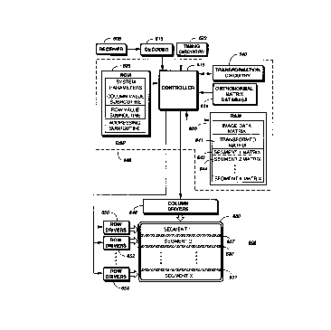
FIG. 6 is an electrical block diagram of an electronic device which
receives and displays image data on an LCD 600, the rows of which are
divided into segments such that the LCD 600 can be addressed using
reduced line addressing techniques, thereby reducing the amount of time,
memorv and power necessary for computation of column voltages. When
the electronic device is a radio communication device 605, as shown, the
image data to be displayed on the LCD 600 is included in a radio frequency
signal, which is received and demodulated by a receiver 608 internal to the
radio communication device 605. A decoder 610 coupled to the receiver
608 decodes the radio frequency signal to recover the image data therefrom
in a conventional manner, and a controller 615 coupled to the decoder 610
further processes the image data.
Coupled to the controller 615 is timing circuitry 620 for establishing
system timing. The timing circuitrv 620 can, for example, comprise a
crystal (not shown) and conventional oscillator circuitry (not shown).
~0 Additionally, a memory, such as a read only memory (ROM) 625, stores
system parameters and system subroutines which are executed by the
controller 615. A random access memory (R~vl) 630, also coupled to the
controller 615, is employed to store the incoming image data as an image
data matrix and to temporarily store other variables derived during
operation of the radio communication device 605.
Preferably, the radio communication device 605 further comprises
an orthonormal matrix database 635 for storing a plurality of orthonormal
functions in the form of a matrix. The orthonormal furctions can be, for
instance, ~Valsh functions, as described above, DCT functions, or PRBS
functions, the number of which must be equal to or greater than the
number of rows included in each segment of the LCD 600 which is to be
addressed. It will be recognized bv one of ordinary skill in the art that,
when Walsh functions are used, the representative Walsh function
matrix (not shown) may actually include a greater number of rows than
necessarv, as Walsh function matrices are available in compiete sets
determined by powers of two.
CA 02126922 1998-09-24
PT00926U (~
In accordance with the preferred embodiment of the present
invention, the LCD 600 is divided into segments which comprise an equal
number of rows. However, unlike LCDs addressed using conventional
reduced line addressing techniques, the LCD 600 includes segments which
overlap. More specifically, each segment of the LCD 600 includes at least
one row 637 which is also included in another LCD segment. For example,
a first LCD segment could include rows one through sixty of the LCD 600,
while a second segment adjacent to the first segment could include rows
sixty through one-hundred-nineteen. In this case, row sixty would be
10 included in both the first and second segments of the LCD 600.
The radio communication device 605 further includes
transformation circuitry 640 for generating column values for addressing
columns of the LCD 600 in accordance with the preferred embodiment of
the present invention. The transformation circuitry 640, which is coupled
15 through the controller 615 to the orthonormal matrix database 635,
transforms subsets of the image data utilizing a set of orthonormal
functions, thereby generating column values. The subsets of the image
data are preferably rows of the image data matrix which correspond to the
rows included in the segments of the LCD 600.
By way of example, when the LCD 600 is divided into first and
second segments, each comprising sixty rows, the first sixty rows of the
image data matrix are transformed using sixty orthonormal functions
stored in the orthonormal matrix database 635, thereby generating a first
set of transformed image data values, i.e., column values. The first set of
25 transformed image data values is a subset of the total number of column
values, which are stored in the form of a "transformed matrix" 641 in the
RAM 630. Thereafter, rows sixty through one-hundred-nineteen of the
image data matrix are transformed using the same sixty orthonormal
functions, thereby generating a second set of transformed image data
30 values for storage as vaIues in the transformed matrix 641. It will be
appreciated that, in this manner, the sixtieth row and any other
overlapping rows 637 will be transformed twice: once during calculations
involving the rows of the image data matrix which correspond to LCD
rows included in the first segment, and once during calculations
35 involving the rows of the image data matrix which correspond to LCD
rows included in the second segment. This procedure is followed until
the entire image data matrix has been transformed utilizing the
21263~2
orthonormal functions stored in the orthonormal matrix database 635, at
which point all of the column values included within the transformed
matrix 6~1 have been generated.
The transformation circuitry 6~0 transforms the image data using
an algorithm such as a Fast Walsh Transform, a modification of a Fast
Fourier Transform, or matrix multiplication. When matrix
multiplication is employed, the transformation can be approximated by
the following equation:
CV = OM ~ I,
wherein I represents the subset of the image data matrix to be transformed,
OM represents a matrix formed from the set of orthonormal functions,
and CV represents the column values generated by the multiplication of
1~ the image data and the orthonormal functions.
Values for driving the rows of the LCD 600 are also generated from
the orthonormal functions, some of which are modified by the controller
61~. ~lore specifically, the controller 615 divides in half the coefficients of
orthonormal functions which correspond to overlapping rows 637 of the
LCD 600 and stores these sets of modified functions in the R~M 630.
When, for instance, the LCD 600 comprises first and second segments, each
having sixty rows, a first row calculation is performed in which the
coefficients of the last orthonormal function are divided by t~.vo because
the last orthonormal function, i.e., the sixtieth orthonormal function,
corresponds to the sixtieth row, i.e., the overlapping row 637, in the first
segment. This first modified set of functions is stored as a first "segment
matrix' 6~2 in the RAM 630. In a second segment row calculation, the
coe~ficients of the first orthonormal function are di~idec~ bv t~o, thereb~T
generating a second set of modified functions, which is stored as a second
segment matrix 6~ in the RAM 630. The first orthonormal function is
modified because, for the second segment of the LCD 600, the first
orthonormal function corresponds to the overlapping row 637, i.e., the
sixtieth row of the LCD 600. It will be appreciated that, if the second
segment includes a second overlapping row 637, such as when the LCD 600
includes a third segment adjacent to and overlapping the second segment,
an orthonormal function corresponding to the second overlappin,, row
63, will also be modified before storage in the second segment matrix 6~.
-
13
This operation is continued until segment matrices corresponding to each
of the LCD segments are calculated and stored in the RAM 630.
According to the present invention, further coupled to the
controller 615 are column drivers 648 for driving columns of the LCD 600
5 with column voltages associated with the column values included in the
rows of the transformed matrix 641. Additionally, row drivers 650, 652,
654 coupled to the controller 615 drive the rows of the LCD 600 with row
voltages corresponding to the columns of the segment matrices 6~2, 644.
Preferably, one set of row drivers 650, 652, 65~ are utilized for each segment
10 of the LCD 600 which is to be addressed.
It will be recognized that the controller 615, the ROM 625, the RAM
630, the orthonormal matrix database 635, and the transformation circuitry
640 can be implemented in a digital signal processor 646, such as the DSP
65000 manufactured by Motorola, Inc. However, in alternate
15 embodiments of the present invention, the listed elements can be
implemented utilizing discrete components. The column drivers 648 can
be implemented using model no. SED1779DOA column drivers
manufactured by Seiko Epson Corporation, and the row drivers 650, 652,
654 can be implemented using model no. SED1704 row drivers, also
20 manufactured by Seiko Epson Corp. However, other row and column
drivers which operate in a similar manner may also be employed.
In accordance with the present invention, the overlapping rows 637
of the LCD 6QO are, as will be described in greater detail below, driven both
with voltages intended for driving a first segment and voltages intended
30 for driving a second segment, wherein the voltages are only half of their
conventional value, i.e., the value associated with the orthonormal
function. Therefore, rather than being turned on when the first segment
is addressed and turned off when the second segment is addressed, as in
the prior art, the rows at the borders of the segments, which are
35 overlapping rows 637, are turned on for twice the conventional time at
half the conventional voltage. This addressing method helps to reduce
sharp discontinuities at the borders of the segments. Additionally, as
,~-
,~ . .
. . CA 02126922 1998-09-24
PT00~26U
14
described above, the rows of the image data matrix which correspond to
the overlapping rows 637 are transformed in two different
transformations during generation of the column values, which further
smooths the display of the image data between the different segments of
the LCD 600. Conversely, in LCDs addressed using conventional methods,
rows at the borders of LCD segments are addressed separately, and the rows
of the image data matrix corresponding to border rows are transformed in
unrelated transformations. As a result, noticeable discontinuities, which
are very undesirable from a user standpoint, are present at the borders of
the different LCD segments.
Referring next to FIG. 7, matrices associated with voltages used in
addressing an LCD 600' are depicted. For illustrative purposes only, the
LCD 600' is shown as including two segments 705, 710 having four rows
each, although it will be appreciated that an LCD of any size and including
any number of segments can be addressed utilizing the addressing method
according to the present invention. As shown, the segments 705, 710
overlap such that row 4 is shared. The rows included in the first segment
705 are addressed with voltages corresponding to a first segment matrix
642, which is calculated in the above-described manner, and the rows
included in the second segment 710 are addressed with voltages
corresponding to a second segment matrix 644. Simultaneously, the
columns of the LCD 600' are addressed with voltages corresponding to a
transformed matrix 641, the values of which have been calculated in a
transformation of the image data by the orthonormal functions stored in
the orthonormal matrix database 635, as described above. The addressing
of the LCD 600' can be better understood by further referencing FIGs. 8-11
in conjunction with FIG. 7.
FIGs. 8-11 are flowcharts illustrating the operation of the controller
615 (FIG. 6) in accordance with the preferred embodiment of the present
invention. Referring to FIG. 8, the controller 615 receives, at step 805,
image data from the decoder 610. The image data is thereafter stored, at
step 810, in the RAM 630 as an image data matrix. Subsequently, the
controller 615 performs, at steps 815, 820, column and row value
subroutines prior to performing, at step 825, an addressing subroutine in
which the LCD 600' is addressed.
Referring to FIG. 9, the controller 615, after storing the image data,
retrieves the orthonormal matrix, which comprises the orthonormal
-
2126~22
1~
functions, from the orthonormal matrix database 635 (FIG. 6~, at step 830.
Additionally, the controller 615 retrieves, at step 835, the image data
matrix from the RAM 630. The orthonormal matrix and rows 1-~ of the
image data matrix are thereafter provided, at step 840, to the
transformation circuitry 640 for transformation thereby to generate
column values in the manner described above. At steps 8~5, 850, the
column values, i.e., the transformed image data values, are received by the
controller 615 and stored as rows 1-~a of the transformed matrix 6~1 (FIG.
7) in the RAM 630. The controller 615 further provides the
transformation circuitry 640 with the orthonormal matrix and ro~s ~-7 of
the image data matrix, at step 855. The transformed image data v alues,
which are received by the controller 615 at step 860, are then stored, at step
86~, as rows ~b-7 of the transformed matrix 6~1 in the RAM 630.
The row value subroutine depicted in FIG. 10 is thereafter
performed bv the controller 615. .~fter retrieving the orthonormal matrix
from the database 635, at step 870, the controller 615 divides, at step 87~, thecoefficients of the last orthonormal function by two to generate a sét of
modified functions, which are stored, at step 880, in the R~I 630 as a first
segment matrix 6~2 (FIG. 7). In a separate computation, the controller 61
divides, at step 885, the coefficients of the first orthonormal function by
two to generate another set of modified functions. This second set is
stored, at step 890, as a second segment matrix 6~.
Once the transformed matrix 6~1 and the first and second segment
matrices 6~2, 6~ have been calculated, the LCD 600' can be addressed, as
shown in FIG. 11. During a first time period, tl, which is an eighth of the
frame duration, the controller 615 provides, at step 900, the first column of
the first segment matrix 6~2 (FIG. 7) to row drivers 650 (FIG. 6!. Row
drivers 650 drive rows 1-~ of the LCD 600' with voltages correspcnding to
the first column of the first segment matrix 6~2 (FIG. 7). .~t the same time,
row 1 of the transformed matrix 6~1 is provided to the column drivers 6~8,
which drive the columns of the LCD 600' with column voltages
approximating the values included in the first row of the transformed
matrix 6~1. Subsequently, during time period t2, the first column of the
second segment matrix 6~ is provided, at step 905, to row drivers 652,
which drive rows ~-7 of the LCD 600' with voltages corresponding to the
values in the first column of the second segment matrix 6~.
Simultaneously, the column drivers 6~8 are provided with row ~b of the
- -
2 1 2 6 3 2 2
16
transformed matriY 6~1. During this time, row drivers 650 are turned off,
i.e., row drivers 650 are provided ~--ith values equivalent to zero volts. It
will be appreciated that, although not specifically recited in the following
description, each set of row drivers 650, 652 is turned off after the time
perlOd IIl Whlrn lt lS use~.
During time period t3, the controller 615, at step 910, provides row
drivers 6~0 with the second column of the first segment matrix 612 and
provides the column drivers 6~8 with row 2 of the transformed matrix
6~1. Thereafter, during time period t~, row drivers 652 receive the second
column of the second segment mat-ix 6~, and the column drivers 6~8
receive ro~ 5 of the transformed matrix 641. This operation continues
through steps 9'70, 925, 930, and 93~ until all of the time periods tl-t8 have
passed, during which the rows of the LCD 600' are addressed with all of the
columns of the first and second segment matrices 6~2, 64~ and the
columns of the LCD 600' are addressed with all of the rows of the
transformed matrix 6~1, as sho~n in FIG. 7.
B~, using the addressing method as described above, discontinuities
between the two segments 705, 710 are reduced. This smoothing effect
occurs because the overlapping row included in both segments 705, 710 is
addressed for twice the conventional amount of time with only half the
conventional voltage, and because rows of the image data matrix
corresponding to the overlapping row of the LCD 600' has been
transformed in two different transformations, thereby avoiding a sharp
transition between column values. For the above example, row ~ of the
image data matrix, which corresponds to the over!apping LCD row, has
been transformed in two different transformations to yield two rows of the
transformed matrix 6~1. This results in a displav which has a much less
abrupt discontinuity between segments than does an LCD addressed u~sing
con~entional reduced line addressing techniques.
As mentioned above, the LCD 600' is shown as having only two
segments 705, 710 (FIG. 7) to simplifv the description of the addressing
method according to the present invention. It will be appreciated,
however, that an LCD having any number of segments can be addressed
using the above-described addressing method, as shown in FIGs. 12 and 13.
FIG. 1~ depicts segments matrices 95~, 951, 952, g53 which are calculated
from a set of four orthogonal functions and which are Lltilized to drive
rows of an LCD 9~5 having - columns and y rows divided into r segments,
I' I ()~)~_h ~ 2 1 2 6 9 2 2
wherein each segment comprises four of the y rows. The ~ourth row of a
first segment matrix 950, which drives, for example, a first segment 9~ of
the LCD 9~5, has been previously calculated by dividing the coefficients of
the fourth orthonormal function by two. The second segment matrix 9~1,
which drives the second segment 958 of the LCD 945, comprises a first row
which has been previously calculated by dividing the coefficients of the
first orthonormal function by two. Additionally, the coefficients of the
fourth orthonormal function have been divided by two to generate the
fourth row of the second segment matrix 951. The first and fourth rows of
the third segment matrix 952 have been similarly calculated, i.e., by
dividing the coefficients of the first and fourth orthonormal functions,
respectively, by two. It will be appreciated that, in the last segment matrix
953, only the first row, which drives the last segment 960 of the LCD 9~
and which corresponds to overlapping row (y-3), is generated by dividing
the coefficients of an orthonormal function bv two. Voltages associated
with the columns of each of the segment matrices 950, 951, 9~', 9~3 are
distributed in time as described above in reference to FIGs. 7 and 11.
FIG. 13 depicts the transform matrix 962 associated with voltages for
driving the ~ columns of the LCD 9~. The transform matrix 96~
preferably includes a single row of values for each row of the image data
matrix which is associated with a non-overlapping row of the LCD 9~5.
Additionallv, for each row of the image data matrix which is associated
with an overlapping row in the LCD 94~, the transform matrix 962
includes two rows, each of which has been generated in a different
transformation. Voltages associated with the rows of the transform matrix
962 are applied to the columns of the LCD 9~ at the different time periods
shown in FIG. 13.
~lthough the previous examples have described LcDc which
include segments having only a single overlapping row, it will be
recognized that the addressing method according to the present invention
can be expanded to address LCDs having segments which include more
than a single overlapping row, thereby further smoothing the
discontinuities at the boundaries of the segments. FIG. 1~ depicts an LCD
970 having two segments 972, 97~ which share two overlapping rows.
first segment matrix 976 for addressing the first segment 972 compr ses
four rows, two of which generated by modifving orthonormal functions.
~Iore specifically, the first and second rows of the first segment matrix 9,6
-
2~26~22
1~
correspond to the first two of a set of four orthonormal functions. The
third row of the first segment matrix 976 is preferably formed by dividing
the coefficients of the third orthonormal function by two, and the fourth
row is formed by dividing the coefficients of the fourth orthonormal
5 function by two. The second segment matri~ 978 also includes four rows.
However, the first two rows, rather than the last two, are generated by
modifying orthonormal functions. The first row of the second segment
matrix 9/8 is formed by dividing the coefficients of the first orthonormal
function by two, and the second row is formed by dividing the coefficients
10 of the second orthonormal function by two.
Similar to the matrices in the above examples, the transform matrix
980 for addressing the columns of the LCD 9~0 includes a single row for
each of the rows of the image data matrix which corresponds to a non-
overlapping row of the LCD 970. Two rows are included in the transform
15 matrix 9S0 for each of the rows of the image data matrix ~ hich
corresponds to an overlapping row of the LCD 970. Therefore, the
transform matrix 980 includes two rows, i.e., rows 3~l and 3~, which have
been generated by transforming the third row of the image data matrix in
two different transformations and two rows, i.e., rows 4n and ~b, which
20 have been generated by transforming the fourth row of the image data
matrix in two different transformation.
It will be appreciated by one of ordinar,v skill in the art that the
addressing method according to the present invention can be easily
adapted for use with other LCDs which combine characteristics of the LCDs
25 described above. For instance, the improved addressing method can be
used for addressing LCDs having both a large number of cegments and a
large number of overlapping row-s between adjacent segments.
In summary, the addressing method described above is employed to
drive LCDs which have been divided into a pl~lrality of segments, each
30 having an equal number of rows. In this manner, the number of
operations required for calculating column voltages for driving columns
of the LCD can be substantially reduced as compared to conventional
active addressing methods. The reduced calculations necessitate less
power consumption, less time, and less space in memorv. Furthermore,
35 in accordance with the present invention, the LCD segments overlap, i.e.,
adjacent segments share rows of the LCD. The row voltages for addressing
overlapping rows of the LCD are consequently calculated by dividing in
2 :1 2 ~ 9 2 2
19
half coefficients of the conventional orthonormal functions used in active
addressing, and the overlapping rows are driven for twice the
conventional amount of time. Additionally, the column voltages for
driving columns of the LCD are generated by transforming, in two
5 different transformation, rows of received image data which correspond to
overlapping LCD rows. In this manner, discontinuities which typically
result from conventional reduced line addressing methods can be
advantageously reduced without sacrificing the reduced power
consumption which results from addressing LCDs in segments. These
10 discontinuities can be even further reduced, therebv smoothing the
display of an image, by increasing the number of overlapping rows in
segments of an LCD.
It will be appreciated by now that there has been provided a method
and apparatus for reducing discontinuities at the boundaries of an active-
15 addressed display which is divided into segments to reduce the number of
necessary addressing calculations.
What is claimed is: