Note: Descriptions are shown in the official language in which they were submitted.
7 ~ 7 0
. ._
VIDEO GRAPHICS CONTROLLER WITH IMPROVED CALCULATION CAPABILITIES
This invention relates in general to computers and more
particularly to a graphics processor with improved calculation
capabilities.
In order to commlln;cate with a user, a computer must be
able to output information to a display.
In a graphics system, the display is defined by an array of
pixels. For example, in a st~n~rd-mode VGA (Video Graphics
Adapter) ~ystem, the screen is addressed as an array of 640 x
480 pixels. Each pixel on the display may be set to a desired
color from a defined palette. Typically 16 or 256 color
palettes are supported. The number of pixels which may be
displayed is defined by the graphic subsystem. Typical VGA
modes support 640 x 480, 800 x 600 and 1024 x 768 resolutions.
VGA modes with resolution greater than 640 x 480 are generally
referred to as "super VGA".
Many of today's application programs are graphics
intensive. For example, a computer-aided design program, such
as AUTOCAD~ by AutoDesk, Inc., Sausalito, California, may spend
a substantial amount of time drawing a figure to the screen. In
some cases, even a small change in the drawing will require the
entire drawing to be redrawn. Consequently, the ability of the
graphics processor to draw line~ quickly becomes of critical
importance.
The problems associated with line drawing have been well
documented for a number of years. Many of these problems are
addressed in an article "Ambiguity in Incremental Line
Rastering", by, ~ack E. Bresenham, IEEE CG&A, Nay 1987, which
may be referred to for further details. The Bresenham article
describes problems in drawing a line using an array of pixels,
since lines having real values between two discrete pixels will
have to approximated using one pixel or the other. Because of
the inaccuracies inherent in approximating the line, issues
concerning the retraceability of lines and the handling
symmetric figures made up of polylines become important.
Consequently, the flexibility of a graphics processor, i.e. the
ability of the graphics processor to facilitate modification of
~ ~ ~ 7 3 7 0
.., ". ,
the line drawing parameters is highly desirable.
Therefore, a need has arisen in the industry for a graphics
processor which provides fast and flexibility processing of
lines and polylines.
In accordance with the present invention, a method and
apparatus for increasing the speed and flexibility of line
drawing in a graphics processor is provided which eliminates
substantial problems with the prior art.
The invention in one aspect provides circuitry for drawing
lines comprised of a plurality of pixels, comprising circuitry
for receiving parameters defining first and second endpoints of
a line, circuitry for calculating line parameters based on the
first and second endpoints, wherein the calculated line
parameters include a line error term which is updated after each
pixel of the line is drawn to determine selection of a next
pixel of the line and circuitry for storing the calculated line
parameters. There is also circuitry for selectively modifying
the contents of the storing circuitry to redefine the calculated
line parameters in response to a control signal prior to
updating the line error term and circuitry for drawing a line
based on the contents of the storing circuitry.
The invention also comprehends a method of drawing lines in
a computer, comprising the steps of receiving parameters
defining first and second endpoints of a line, calculating line
parameters defining a line based on the first and second
endpoints, wherein the calculated line parameters include a line
error term which is updated after each pixel of the line is
drawn to determine selection of a next pixel of the line,
respon~ive to a control signal, selectively allowing line
parameters to be modified prior to drawing a line based on the
line parameter~ and prior to updating the line error term or
drawing a line based on the calculated line parameters without
modification of the line parameters.
Further the invention pertains to a computer system
comprising a central processing unit, a display and a graphics
processor for drawing a line comprised of a plurality of pixel~
coupled to the central processor and the display, the graphics
processor including the circuitry referred to above.
WO93/14~8 ~1 2 7 ~ 7 ~ PCT/US93/~K22
The present invention provides significant
advantages over the prior art. Because the CPU may
modify the parameters before the line is draw by the line
draw engine, significant flexibility is provided by the
graphics processor. The CPU may, for example, adjust the
parameters to generate a desired pattern, to vary the
length of the line, or to cure a slope-related problem.
BRIEF DESCRIPTION OF THE DRAWINGS
For a more complete understanding of the present
invention, and the advantages thereof, reference is now
made to the following descriptions taken in conjunction
with the accompanying drawings, in which:
FIGURE l illustrates a block diagram of a typical
computer system;
FIGURE 2 illustrates a block diagram of the graphics
subsystem of the present invention;
FIGURE 3 illustrates a block diagram of the portion
of the graphics processor involved in line processing;
FIGUREs 4a-d illustrate examples of different line
possibilities using discrete pixels;
FIGURE 5 illustrates a diagram of the registers used
in the line draw engine;
FIGURE 6 illustrates a diagram of the octant sign
codes;
FIGURE 7 illustrates a flow chart of the operation
of the line draw engine;
FIGURE 8 illustrates a rendering of a curve using
multiple line segments;
FIGURE 9 illustrates a flow chart describing
coordinate buffering; and
FIGURE l0 illustrates a flow chart describing line
pattern features.
WOg3/l~K8 PCT/US93/~622
21~737~ 4 '~
DETAILED DESCRIPTION OF THE INVENTION
The preferred embodiment of the present invention
and its advantages are best understood by referring to
FIGUREs 1-10 of the drawings, like numerals being used
for like and corresponding parts of the various drawings.
SYSTEM CONFIGURATION
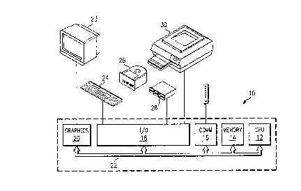
FIGURE 1 illustrates a block diagram of the general
architecture of a typical computer system. The computer
system 10 comprises a CPU 12, memory 14, communications
interface 16, input/output (I/O) interface 18 and
graphics circuitry 20. The various subsystems 12-20
communicate over a bus 22. The graphics subsystem 20
outputs data to a display 23, the I/O subsystem 18
communicates with keyboard 24, hard disk 26, floppy disk
28, and printer 30. Communications subsystem 16
transmits and receives data over telephone lines. While
the computer system of FIGURE 1 illustrates many of the
components of a typical computer system, other
components, such as CD-ROMs, sound processing cards, and
so on, may also be utilized in the computer system 10.
GRAPHICS SUBSYSTEM
FIGURE 2 illustrates a block diagram of the graphics
subsystem 20. The graphics subsystem 20 comprises
graphics processor 32, which is coupled to bus interface
circuitry 34, frame buffer memory subsystem 36 and
digital-to-analog (DAC) subsystem 38. The bus interface
34 comprises bus control interface 40, Boot/Control ROM
42, address interface 44 and data interface 46. Bus
control interface 40 is coupled directly to the graphics
processor 32. Boot/Control ROM 42, address interface 44
and data interface 46 are coupled to the graphics
processor via bus 48. Boot/Control RON 42 is enabled via
WO93/14~ 2 ~ 2 7 ~ PCT/US93/~622
graphics processor 32. Bus 48 is also coupled to clock
generator 50 which provides a clock signal to the DAC 38.
DAC 38 is also coupled to graphics processor 32 and to
the serial shift registers of frame buffer 36. The
serial shift registers of frame buffer 36 are also
coupled to graphics processor 32 via multiplexer 52.
Frame buffer 36 receives address, data and control
signals from graphics processor 36 over address bus 54,
data bus 56, and control bus 58, respectively. Frame
buffer 36, in the preferred embodiment, comprises a
plurality of video RAMs (VRAMs) arranged in two banks tA
and B~, each bank comprising four planes. Each plane
provides an 8-bit pixel; thus, each bank outputs data in
32-bit words.
The frame buffer 36 stores the pixel data for each
addressable location on the screen. The serial shift
registers of the frame buffer memory system 36 serially
ouL~u~ the pixels to the DAC 38, which converts the
digital value of each pixel to an appropriate signal for
display by the monitor.
LINE DRAW Facility
An important aspect of the graphics processor 32 is
the line draw facility. A block diagram of the portion
of the graphics processor involved in line processing is
illustrated in connection with FIGURE 3. A line draw
facility 60 is coupled to memory controller 62, memory
address generator 64, datapath circuitry 66, and bus
interface 34. The memory controller 62 receives memory
cycle requests from the line draw facility 60, Bit Block
Transfer (BLT) engine (not shown) and bus interface 34
and supplies control signals (RAS, CAS, OE and WE) to the
frame buffer 36 responsive thereto. The memory
controller 62 also provides acknowledge signals to the
requesting component.
WO93/14~8 PCT/US93/~622
212737~ 6
The memory address generator 64 supplies the
appropriate addresses based on control inputs from the
line draw facility 60, BLT engine and bus interface 34,
and outputs addresses to the frame buffer 36.
The datapath circuitry 66 enables communication with
the frame buffer under control of the memory controller
62, which arbitrates between requests from the line draw
facility 60, BLT engine and bus interface 34 (which
passes data requests to and from the CPU 12). The
datapath circuitry 66 receives mask and control signals
from the line draw facility 60 and transfers and receives
data to and from the frame buffer 36. The CPU may also
read from and write to registers in the line draw
facility 60 via the bus interface.
The graphics processor 32 provides control signals
to the line draw facility 60 including a system clock
signal, a reset signal, and the number of bits per pixel.
The line draw facility 60 enhances the performance
of the graphics processor while drawing lines by off-
loading calculations from the CPU 12 and computing the
individual pixel addresses constituting a line in the
line draw facility 60. In the preferred embodiment, the
line draw facility 60 is based on the Bresenham line
drawing algorithm described in detailed in J. E.
Bresenham, "Algorithm for Computer Control of a Digital
Plotter", IBM Systems J., Jan. 1965, pp. 25-30. The
following C language program describes computation of the
Bresenham parameters. In this program, "xO" and "yO" are
the coordinates of the starting point of the line, "xl"
and "yl" are the coordinates of the ending point of the
line, and "Constl", "Const2" and "error" are line
parameters calculated as part of the Bresenham algorithm.
W093/14468 2l2'737a PCI/US93/00622
'~_................................. 7
TABLE I
LINE DRAW ALGORITHM
s void line function()
intxO,yO,xl,yl
{
int dx, dy, Constl, Const2, error, x, y, length;
int x is major, inc x, inc_y;
dx = abs(xl - xO); /* C~lcul~te the variables */
dy = abs(yl - yO);
x_is major = (dx >= dy);
inc x = (xl > xO);
inc y = (yl > yO);
if (x_is major)
C3nstl = dy < < 1; /~ ' < < ' is shift It is the same as *2 */
Const2 = Constl - (dx << l);
Length = dx + l;
error = Constl - dx;
}
else
{
Constl = dx << l;
Const2 = Constl - (dy << l);
length = dy + l;
error = Constl - dy;
}
x = xO; y = yO;
SetPixel( x, y, Color); /* Turns on first pixel */
while (--length > O)
{
if (x_is_major)
if (inc_x)
x++;
4 ~ else
x--;
else
if (inc y)
Y++;
4 5 else
y__;
WO 93/14468 ~ ~ PCI/US93/00622
212r~37a 8
if (error < 0)
error += Constl;
else
{
if (x is_major)
if (inc_y)
Y++;
else
y__;
lo else
if (inc x)
x++;
else
x--;
error += Const2;
}
SetPixel( x, y, Color); /~ Turns on a pixel ~/
}
}
The Bresenham algorithm defines each line by four
parameters~ X0, Y0, X1, Y1 (corresponding to xO, yO, xl
and yl of the C program defined above). X0 and Y0 define
25 the start point (P0) and X1 and Y1 define the end point
(P1). The line draw facility 60 calculates the Bresenham
parameters - the line error term ("error" from the C
program), K1 (Constl from the C program) and K2 (Const2
from the C program).
~n the preferred embodiment, the line draw facility
60 uses an XY coordinate system with (0,0) being the
upper-lefthand corner of the screen. The line draw
facility 60 draws pixels of a line by storing an
appropriate color code in an address of the frame buffer
memory subsystem 36 corresponding to a desired pixel.
When the line draw facility 60 draws pixels of a line, it
always increments the pixel address in the major
direction. The major direction is the X direction if
¦X1 XOI > ¦Y1 YOI and is in the Y direction if ¦Y1-YO¦ >
¦X1 XOI. The direction which is not the major direction
~l27~7~
WO 93/14468 PCr/US93/00622
~ ,~, 9
is referred to as the minor direction. The pixel
addresses forming a line will always be axial
(incremented in the major direction) or diagonal
(incremented in both the major and minor directions).
The line drawing facility 60 will never write to adjacent
pixels in the minor direction within one line drawing
operation. Consequently, a line draw from (0,0) to
(10,0) will have the same number of pixels as a line that
runs from (0,0) to (10,5), even though the second line is
geometrically longer by a factor of 1.414. Since both
lines have equal magnitudes in the major direction, the
number of pixel steps for each line is identical.
Examples of different lines drawn in this fashion from
(0,0) to (4,2) are illustrated in FIGUREs 4a-d.
In FIGURE 4a, the pixel steps are DAAD, where "D"
defines a diagonal step and "A" defines an axial step.
In FIGURE 4b, the steps are DADA, in FIGURE 4c, the steps
are ADDA, and in FIGURE 4d, the steps are ADAD. In many
instances, the particular pixels implementing the line
are unimportant. However, in some instances, such as
where parallel lines are drawn, it is desirable to have
the same relative pixels addressed for each of the
parallel lines. In other instances, the "reversibility"
of a line is important. A line is reversible if the
pixels comprising the line are the same for both the line
drawn from P0 to P1 and the line draw from P1 to P0. The
reversibility of the line may be important, for example,
where a line is erased by writing the background color to
the pixel addresses of a line drawn to P1 to P0. If the
line is not reversible, residual pixels will be left
after the erasure. Another instance requiring
reversibility is where a polygon is traversed in one
direction, then traversed in the opposite direction.
LINE DRAW REGISTERS
WO93/14U~ - PCT/US93/~K22
212~370 lO
FIGURE 5 illustrates a diagram of the registers used
in the line draw facility 60. The line draw facility 60
includes the P0 coordinate registers (XO, Y0), the P1
coordinate registers (X1, Y1), pattern registers (Line
Pattern, Pattern Pointer, Pattern End Pointer), line
parameter registers (Line Error Term, Line Pixel Count,
Octant, Sign Code, K1 and K2) and a control register (Line
Command Bits). Each bit of the Line Command Bits
register corresponds to a control code: Start, Calc_Only,
Last_Pixel_Null, Keep_X0/Y0, Retain_Pattern_Pointer,
Reversible_Line, Axial_When_0, and Line_Reset. Registers
are defined below, with addresses as used in connection
with a VGA graphics subsystem. Addresses and registers
sizes may change upon the implementation of the graphics
subsystem.
TABLE II
LINE COMMAND, 3CF.60h (8 bit, R/W)
BIT DESCRIPTION
7 Line_Reset. Toggling this bit (set to 1, then
set to 0) places the line draw facility 60 into
a known state. It will interrupt a line draw
operation if one is executing. This bit must
be cleared (set to 0) by the controlling
process before using the line draw facility 60
and before setting any other control bits in
the register. Specifically, the following
state is set:
*Line Pattern Register bits set to all
l's.
*Pattern Pointer Register set to 31.
*Pattern End Pointer Register set to 0.
*Constant Register l(Kl) and Constant
Register 2(K2) both set to 0.
*Line Error Term Register set to 0.
*Pixel Count Register set to 0.
*Sign Codes Register set to 0.
*Facility 60 placed in ready state.
The datapath state is not affected by setting
this bit.
6 Axial_When_0. This bit provides control for
movement in the direction of the minor axis
WO93/14~ PCT/US93/~K22
11~
when the computed error term for the next pixel
to be drawn equals 0. When set to 1, this bit
causes the line draw facility 60 to step only
in the direction of the major axis when the
error term for the next pixel equals 0. When
set to 0, the line draw faci~,ty 60 steps in
both the major and minor axis direction when
the error term for the next pixel equals 0.
Reversible Line. When this bit is 0, the
Axial_When 0 bit controls the line draw
facility 60 for the case when the error term
equals 0. When this bit is 1 then the
Axial_When 0 setting is ignored. Instead, the
Sign of Delta X bit in the Sign Codes Register
(3CF.63h) controls the action of the line draw
facility 60 for the case when the error term
equals 0. When the Sign of Delta X bit is 0,
then the line draw facility 60 will move in the
direction of the minor axis when the error term
equals 0. When the Sign of Delta X bit is 1,
then the line draw facility 60 only moves in
the direction of the major axis when the error
term equals 0.
4 Retain Pattern_Pointer. This bit specifies
that the value of the Pattern Pointer Register
is not to be reset to 31 at the end of the next
line draw operation. Normally, the Pattern
Pointer Register is reset to 31 at the end of
each line draw operation.
3 Keep X0/Y0. When set to 1, this bit specifies
that both X0 and Y0 registers not be updated to
the coordinates of the last pixel of the line
drawn. Since the Line Pixel Count Register may
be modified prior to performing a line draw,
the last pixel of a line may have different
coordinates then those stored in the X1, Y1
registers.
2 Last Pixel Null. When set to 1, this bit
specifies that the last pixel of a line is no~
to be written to the frame buffer. The valu~s
of the Pattern Pointer Register and Line Error
Term Register are still set as if the pixel was
drawn.
1 Calc_Only. This bit places the line draw
facility 60 in a mode where only the line draw
parameters are calculated and the line draw
facility 60 stops. Line drawing will not
WO93/14#~ ~ ' PCT/US93/~622
21273~0 12
proceed automatically in this mode. The line
drawing function must be started manually with
the Start bit. This mode is used when the line
draw parameters error term, pixel count, and
major/minor axis sign codes must be accessed.
The calculation of parameters based on the
settings of the X and Y coordinate registers
takes effect only when Yl is written after this
bit is set.
0 Start. When set to 1, the line draw facility
60 starts drawing a line as defined by the
current line draw parameters. This bit also
indicates the status of the current line draw
operation. It will be set to 0 when the line
draw facility 60 has finished drawing the
current line. Once started, the line draw
facility 60 cannot be aborted except by
toggling the Line Reset bit.
TABLE III
PATTERN POINTER, 3CF.61h (5 bit, R/W)
BIT DESCRIPTION
7-5 Reserved (0).
4-0 Pattern Pointer.
The Pattern Pointer register shown in Table III uses
a 5-bit value (decimal 1-31) to indicate the bit position
in the Line Pattern Register whose contents will be used
to generate the next pixel. At reset (including Line
Reset) and at the end of each line draw operation, it is
reset to 31. During pixel generation, it is decremented
by 1 for each pixel count. ~esetting of the value to 31
at the end of each line draw operation can be inhibited
with the Retain Pattern_Pointer bit in the Line Command
Register.
The value in this register may be set before drawing
a line to indicate the bit position in the Line Pattern
WO93/14~ PCT/US93/00622
2127370
13
Register to use when beginning the next line draw
L operation.
TABLE IV
PATTERN END POINTER, 3CF.62h (5 bit, R/W)
BIT DESCRIPTION
7-5 Reserved (0).
4-0 Pattern End Pointer.
The Pattern End Pointer register described in Table
IV specifies the effective length of the line pattern by
indicating the lower bit position of the Line pattern
Register. Thus, if the Pattern End Pointer Register is
k, then the pattern bits from 31 to k will be used during
line rendering. Its initial value after power-up or
reset is 0.
TABLE V
OCTANT SIGN CODE, 3CF.63h (8 bit, Read/Write)
BIT DESCRIPTION
7-3 Reserved. (Write and read back 0's)
2 Sign of Delta X. (0 = Positive, 1 =
Negative)
1 Sign of Delta Y. (0 = Positive, 1 =
Negative)
0 Major Axis. (Sign of (¦Delta X¦ - ¦Delta
Y ~
The Octant Sign Code register described in Table V
contains the major/minor axis sign codes, which describes
the slope of a line. This register is set by the line
draw facility 60 when the Y1 Register is written. FIGURE
6 shows the sign code to octant mapping.
WO93/14~8 ~1 2 7 3 7 -O 14 PCT/US93/~622
TABLB VI
LINE PIXEL COUNT, 3CF.64,65h (16 bit, Read/Write)
PIXELS DRAWN
PIXEL COUNTLPN = 0 LPN = 1
0
1 2
2 3 2
n n+l n
BITS DESCRIPTION
15-10 Don't care.
9-0 Pixel count (unsigned).
The Line Pixel Count register described in Table VI
contains the pixel count for the line draw facility 60.
The value stored in this register is a 10-bit unsigned
number interpreted as: "number of pixels to be drawn" -
1. This is the difference of the coordinate endpoints of
the line for the major axis coordinates. Table VI
indicates the number of pixels drawn based on the value
of this register and the Last_Pixel Null (LPN) bit
setting. This register is set by the line draw facility
60 when the Yl Register is written.
TABLB VII
LINE ERROR TERM, 3CF.66,67h (16 bit, R/W)
BIT DESCRIPTION
15-12 Reads back the sign extension of bit 11.
11-0 Error Term (signed).
The Line Error Term register defined in Table VII
specifies the initial error term to be used by the inner
loop of the line draw algorithm. The value is a 12-bit,
two's complement quantity for values in the range
W093/14K8 PCT/US93/~622
2127~
~ - 15
t-2048..2047]. Negative values are sign extended to bits
t15..12] on a read operation. The value is calculated
from (2*dMinor-dMajor) where dMinor is the dimension of
the minor axis and dMajor is the dimension of the major
axis. Programming of this register to draw lines is
optional. If not supplied then the hardware will
generate the error term required for generation of the
line. Setting this register allows the host software
initial control of the pixel movement in minor axis
direction of line generation. In use, the software would
set the value of this register after writing the X and Y
coordinate registers when the Calc_Only bit has been set
in the Line Command Register. This register is set by
the line draw facility 60 when the Yl Register is
written. At the end of a line draw operation, this
register gets set to the value of the error term for the
last pixel drawn.
TABLE VIII
Kl CONSTANT, 3CF.68,69h (R/W)
BIT DESCRIPTION
15-11 Reserved. (Write and read back zeros.)
10-0 Kl (unsigned).
The Kl register described in Table VIII specifies
the line draw parameter constant K1. The value K1 is
calculated as 2*dMinor where dMinor is the dimension of
the minor axis. This is an 11-bit unsigned quantity.
This register is set by the line draw facility 60 when
the Y1 Coordinate Register is written.
WO93/l4~ PCT/US93/~K22
2~27370 16 ~
TABLF IX
K2 CONSTANT, 3CF.6A,6Bh (R/W)
BIT DESCRIPTION
15-12 Reads back the sign extension of bit 11.
11-0 K2 (signed).
The K2 register described in Table IX specifies the
line draw parameter constant K2. the value K2 is
calculated as (2*dMinor - 2*dMajor) where dMinor is the
dimension of the minor axis and dMajor is the dimension
of the major axis. This is a 12-bit two's complement
signed quantity. On read-back, bit 11 is sign extended
to bits 15-12. This register is set by the line draw
facility 60 when the Yl Coordinate Register is written.
TABLE X
X0, 63CO, 1 (16 bit, R/W)
BIT DESCRIPTION
15-10 Don't care.
9-0 Starting X point (0 > = X0 > = 1023).
The X0 register described in Table X specifies the X
coordinate of the line start point. Legal values are in
the range 0 to 1023. On power-up or reset, this register
is set to 0. The value in this register is not affected
by a Line Reset.
WO93/14~ 2 l ~ 7 3 7 ~ PCT/US93/~622
17
TABLE XI
Y0, 63CX2, 3 (16 bit, R/W)
BIT DESCRIPTION
15-10 Don't care.
9-0 Starting Y point (0 > = Y0 > = 1023).
The Y0 register described in Table XI specifies the
Y coordinate of the line start point. Legal values are
in the range 0 to 1023. On power-up or reset, this
register is set to o. The value in this register is not
affected by a Line Reset.
TABL~ XII
LINE PATTERN, 83CO, 1,2,3, (32 bit, R/W)
BIT DESCRIPTION
31-0 Line pattern.
The Line Pattern register described in Table XII
denotes the pattern of the line drawn to the frame
buffer. A "1" bit in this register specifies that a bit
value of 1 is to be written to the datapath and expanded
to a pixel. A "1" bit in the Line Pattern Register
usually represents foreground color pixel. A "0" bit in
this register specifies that a bit value of 0 is to be
written to the datapath. A "0" bit usually represents a
background color pixel. This register is initialized to
l's on power-up and reset.
WO93/1~K8 PCT/US93/~K22
2127370
18
TABLE XIII
Xl REGISTER, 83CC,D (16 bit R/W)
BIT DESCRIPTION
15-lO Don't care.
9-0 Ending X point (0 > = Xl ~ = 1023).
The Xl register described in Table XIII specifies
the X coordinate of the line end point. Legal values are
in the range 0 to 1023. On power-up or reset, this
register is set to 0. The value in this register is not
affected by a Line Reset.
TABLE XIV
Y1 REGISTER, 83CE,F (16 bit, R/W)
BIT DESCRIPTION
15-10 Don't care.
9-0 Ending Y point (0 > = Yl > = 1023).
The Y1 register described in Table XIV specifies the
Y coordinate of the line end point. Legal values are in
the range 0 to 1023. On power-up or reset, this register
is set to 0. The value in this register is not affected
by a Line Reset.
Writing to this register address causes the line
draw facility 60 to start automatically. If the
Calc_Only bit is set in the Line Draw Command Register,
then a write to this address causes the line draw
facility 60 to calculate the line draw parameters and
then wait. For byte accesses to this register, both
bytes must be written to cause the line draw facility 60
to start automatically.
AUTO-START/CALC-ONLY/POLYLINES
WO93/14U~ 2 ~ 2 7 3 7 ~ PCT/US93/~622
19 ~
The line draw facility 60 provides a number of
features which increase the speed and enhance the
flexibility of line drawing. FIGURE 7 illustrates a flow
chart describing the Auto-Start, Calculate-Only and
Polyline modes of operation for the line draw facility
60. In decision block 70, the Start bit of the line
command register is reviewed. If the start bit is set to
"1", the line draw facility 60 begins drawing a line as
defined by the current line draw parameters stored in the
registers of FIGURE 5. If the Start bit is set to "0",
then the line draw facility 60 waits until the Y1
coordinate is written to the Y1 register in decision
block 72. Thus, the line draw facility 60 waits until
either the Start bit is set to "1" (decision block 70) or
Y1 is written to the Y1 register (decision block 72). If,
in decision block 72, the Y1 coordinate has been written
to the Y1 register, then the line parameters described
above are calculated in block 74. After the line
parameters have been calculated (and stored in the
appropriate registers shown in FIGURE 5), the line draw
facility 60 determines whether the Calc_Only bit is set
to "0" in decision block 76. If the Calc_Only bit of the
Line Command register is set to "0", the line is drawn in
block 78. If the Calc_Only bit is set to "1" in decision
block 76, the line draw facility 60 waits until the Start
bit of the Line Command register is set to "1" in
decision block 80 before drawing the line in block 78.
After drawing the line, the line draw facility 60 checks
the Keep X0/Y0 bit in decision block 82. If the
Keep_X0/Y0 bit is set to "0", then the P1 coordinates (X0,
Y0) are set to the current pixel coordinates, i.e., the
last pixel of the line, in block 84. As described below
with regard to the Calculate-Only mode, the last pixel of
a line may be different than the pixel defined by the X1,
Y1 registers. This feature facilitates the drawing of
WO93/14468 PCT/US93/~622
2 1 2 7 ~ 20 ~~
polylines, where a pixel is shared between the last pixel
of a first line and the first pixel of a second line.
As described in FIGURE 7, the line draw facility 60
provides significant speed and flexibility enhancements.
The speed increase is perhaps best understood in
connection with FIGURE 8 which illustrates a curve drawn
as a series of connected lines 86. Each line 86 is
bounded by end points 88. In the prior art, the drawing
of each line 86 would require at least three bus cycles
prior to drawing each line - one bus cycle for writing
the P0 coordinate (assuming that X0 and Y0 are written
simultaneously), one bus cycle for writing the P1
coordinate, and one bus cycle for instructing the
graphics processor to begin the line draw operation.
When a number of lines must be drawn, the additional
clock cycle for instructing the graphics processor to
begin the line draw operation presents a significant
overhead. It should be noted that in a high resolution
graphics program, the number of lines used to implement a
curve would be much greater than that shown in FIGURE 8.
Thus, the time savings attributable to the Auto-Start
feature may be significant.
Further, it should be noted from FIGURE 8 that the
end points 88 between lines are shared, i.e., the last
pixel of one line becomes the first pixel for the next
line. The Polyline features, where the last pixel
coordinate (P~) is automatically written to the X0 and Y0
registers, further increases the speed of drawing lines.
In this mode, in conjunction with the Auto-Start mode,
the host program need only write to the X1 and Y1
registers to begin drawing the next line segment. It
should be noted that while the Y1 register has been
chosen in the illustrated embodiment to initiate the line
draw process, either the X1 or Y1 registers could be used
for this purpose.
WO93/1~8 2~,73~a PCT/US93/~K22
21
The Calculate-Only mode provides significant
flexibility in using the line draw facility 60. As shown
in FIGURE 7, when the Calc_Only bit is set to "1", the
line draw facility 60 calculates the line parameters in
block 74, but does not proceed with drawing the line in
block 78 until the Start bit is set to "1". This allows
the host program to modify the parameters prior to
drawing the line. While the preferred embodiment of the
line draw facility 60 provides for some adjustment of the
method by which the lines are drawn, i.e., through the
Axial_When_0 and Reversible_Line controls bits of the
Line Command register, there may be instances in which
further control of the line draw parameters is desired.
The parameters which may be modified in the Calculate-
Only mode are the Line Error Term, Kl and K2 Constants,Octant Sign Code and Line Pixel Count. These parameters
are held in the registers shown in FIGURE 5 and are
described hereinabove. The line draw facility 60, in the
preferred embodiment, uses these five parameters to draw
a line. It should be noted that the end point
coordinates (X1, Y1) are not needed to draw the line, but
are used to calculate the intermediate parameters. The
Line Pattern, Pattern Pointer, and Pattern End Pointer
registers are used to determine what value will be
written to the frame buffer 36 for each pixel in the
line. The pattern functions of the line draw facility 60
are described in greater detail hereinbelow.
The Calculate-Only mode may be used in a variety of
operations. For example, it may be desirable to draw a
line of a predetermined length using the slope of a line
from (0,0) to (20,18) even though the line will not span
the entire length between these two coordinates. In the
line draw facility 60 of the present invention, the
Calc_Only bit could be set to "1" and the coordinates for
P0 and P1 could be written to the appropriate registers as
~1 ~7~7~ -
22
(0, O) and (20, 18). The line draw facility 60 would then
calculate the line parameters upon receiving the Y1 coordinate.
Thereafter, the value of the Line Pixel Count register could be
modified to set the line to the desired length.
Another use of the Calculate-Only mode would be to bias the
line error term based on the octant (stored in the Octant Sign
Code register) to modify which pixels are used to implement a
given line. Several algorithms exist for implementing
reversible lines and by setting the Line Pixel Count to "1", the
Line Error Term register could be modified after each pixel is
drawn. The Calculate-Only mode could be used to calculate the
parameters and modify the line error term to a desired value.
The Calculate-Only mode could also be used to provide CPU
generated patterns. For example, a dashed line between two
points may be desired, with a solid portion terminating on each
of the endpoints. To provide a constant slope to the dashes,
the parameters for each dash could be computed using the
parameters for the line between the endpoints of the overall
line. The CPU would compute the number of pixels of each
segment and adjust the Line Pixel Count register accordingly.
With the Reep-XO/YO bit set to IIO", the X0 and Y0 registers will
be set to the end of the segment after it is drawn. The pattern
in the pattern register can then be changed (from "111 ... 111"
for the foreground color segments to "000 ... 000" for the
background color segments) and the Line Pixel Count register may
be set to the desired length of the blank segment. The blank
segment is drawn when the Start bit is set to "1". These steps
may be repeated for each segment of the dashed line. For ease
of coding, the Last_Pixel_Null bit can be set to "1" and the
Line Pixel Count register can be set to a value which is one
greater than the number of pixels desired.
WO93/1~8 2 1 2 7 3 ~ O PCT/US93/~622
23
A third aspect of the present invention which
provides additional flexibility is the ability of the
host application to set all of the parameters (except for
the P1 registers) and write the parameters to the
appropriate registers. By setting the Start bit at block
70, the line will be drawn in block 78 using the values
stored in the parameter registers without the
intermediate calculation of line parameters in block 74.
~u~KING COORDINATES
FIGURE 9 illustrates a flow chart illustrating the
buffering features of the line draw facility 60. In
decision block 90, the host application determines
whether or not polylines are to be drawn. If so, the
Keep_X0/Y0 bit of the Line Command register is set to "0"
in block 92, otherwise, if polylines are not to be
written, the state of the Keep_X0/Y0 bit is unimportant.
In block 96, the P0 and P1 coordinates are written to the
X0, Y0, X1 and Y1 registers. The line draw operation will
then continue as described in connection with FIGURE 7.
However, prior to ending the line draw operation, the
host application may write the next set of coordinates to
the X0, Y0, X1 and Y1 registers prior to the end of the
line draw operation. Thus, in decision block 98, the
host application checks the Buffer_Busy bit (which is
available in Datapath circuitry 66) to determine whether
the buffer is busy. The Buffer_Busy bit is set to a "l"
when the line draw facility 60 is drawing a line and
coordinates have been received by the line draw facility
60 for the next line. If the Buffer_Busy ~it is set to
"0", the coordinates for the next line may-be written to
the P0 and P1 registers in block l00. If the operation is
a polyline operation, the host application need write
only to the X1 and Y1 registers, requiring fewer
transactions than the general endpoint line draw case.
WO93/14U~ PCT/US93/~K22
24 _~
212 ~3 ~
Otherwise, if the buffer is busy in decision block 98,
the host application will wait until the Buffer_Busy bit
is set to "0". When buffering, the line draw facility 60
cannot be started manually and the Calculate-Only mode
can be initiated, but the contents of the register are
not valid until the line draw facility 60 is free.
In normal use, the parameter registers may not be
programmed with new values until the line draw facility
60 completes its current operation, forcing a
serialization of parameter-writing and line drawing
operations. When the line draw facility 60 completes its
operation, the Start bit is set to "0". This status bit
indicates when the line draw facility 60 may be
programmed. However, to use buffering, the software need
only check the Buffer_Busy bit, and therefore may set the
coordinate registers prior to completion of the line draw
operation, providing for an overlap of parameter-writing
and line drawing operations.
PAll~K~D LINES
The line draw facility 60 treats all lines as
pattern lines. For each pixel in a line, the Line
Pattern register determines whether a foreground or
background pixel will be written to the frame buffer 36.
If the bit in the pattern is a "1", the value stored in a
foreground color register (not shown) is written to the
frame buffer 36 and if the bit is a "0", the value stored
in a background color register (not shown) is written to
the frame buffer 36. The foreground and background color
registers are located in the datapath circuitry 66.
Operation of the line draw facility 60 with regard
to pattern lines is illustrated in connection with FIGURE
10. In block 102, the pixel color is set to the value
indicated by the bit of the Line Pattern register at the
position indicated by the Pattern Pointer register. For
WO93/14~ 2 1 2 ~ PCT/US93/~622
a 32-bit line pattern register, the pattern pointer will
7, start at "31" and decrement to "0", under normal
operation. In decision block 104, the line draw facility
60 determines whether the Last_Pixel_Null bit of the line
command register is set and whether the current pixel is
the last pixel in a line. If either the current pixel is
not the last pixel in the line or if the Last_Pixel_Null
bit is set to "0", then the pixel color determined in
block 102 is written to the frame buffer 36 in block 106.
As described below, the write to the memory may involve a
raster operation. If the Last_Pixel_Null bit is set to
"1" and the current pixel is the last pixel, then the
line draw facility 60 does not write to the frame buffer
36. In decision block 108, the line draw facility 60
determines whether the current pixel is the last pixel in
the line. If the current pixel is the last pixel, the
line draw facility 60 checks to see if the Retain_Pattern
bit of the Line Command register is set to "0". If so,
the Pattern Pointer register is reset to "31" (for a 32-
bit Pattern Pointer register) in block 112. If theRetain Pattern bit is set to "1" in decision block 110,
or if the current pixel is not the last pixel in decision
block 108, then the line draw facility 60 checks to see
whether the value stored in the Pattern Pointer register
is greater than the value stored in the Pattern End
Pointer register in decision block 114. If not, the
Pattern Pointer register is reset to "31" in block 112.
If the value stored in the Pattern Pointer register is
greater than the value stored in the Pattern End Pointer
register in decision block 114 and if the current pixel
is not the last pixel of a line with the Last_Pixel_Null
bit set to "1" in block 115, then the Pattern Pointer
register is decremented in block 116. Program control
returns to block 102 where the next pixel in the line is
set to the value indicated by the bit in the Line Pattern
WO93/14~ ~ PCT/US93/~K22
21~7~70 26
register indicated by the new value of the Pattern
Pointer register. If the current pixel is the last pixel
of the line and the Last_Pixel_Null bit is set to "1",
then the Pattern Pointer register is not decremented.
The Pattern End register provides cycling of bits
comprising all or part of the Line Pattern register. For
example, a desired pattern may alternate between seven
foreground pixels and seven background pixels. In this
case, bits 25-31 of the Line Pattern register would be
set to "1" and bits 18-24 of the Line Pattern register
would be set to "0". The Pattern End Pointer register
would be set to "18".
The Retain_Pattern bit specifies whether the pattern
will continue over two or more lines. In other words, if
the Retain_Pattern bit is set to "1", the pattern defined
by the line pattern register and the pattern end pointer
will continue over polylines, without resetting the
Pattern Pointer register to "31" at the end of each line
segment.
The Last_Pixel_Null bit specifies whether the last
pixel of a line will be written to the frame buffer 36.
The use of this control bit pertains mainly to raster
operations polylines, where the last pixel of the first
line is the first pixel of the subsequent line. Writing
to the frame buffer 36 is controlled by a raster
operation code register. The value stored in the raster
operation code register defines a logical operation which
will be performed on the source pixel (the pixel value
determined in block 102) and the corresponding pixel
already stored in the frame buffer. If a raster
operation is specified, the datapath circuitry performs a
read-modify-write operation, wherein the destination
pixel is retrieved from memory, the logical operation
with the source pixel and the result is stored to the
frame buffer.
WO93/1~8 2 ~ ~ 7 3 ~ iJ PCT/US93/~K22
27
TABLE XV
Raster Operation Codes
5Reqister Value Raster Operation
0000 0
0001 !(D + S)
0010 D & (!S)
0011 !S
0100 (!D) & S
0101 !D
0110 D XOR S
0111 !(D & S)
1000 D & S
1001 D XNOR S
1010 D
1011 D + (!S)
1100 S
1101 (!D) + S
1110 D + S
1111 1
Legend: D = Destination
S = Source
! = Not
& = And
+ = Or
Where logical operations are performed on the frame
buffer memory, writing to the same pixel location twice
may cause unintended effects. Hence, the Last_Pixel_Null
status bit prevents the raster operations from being
performed twice on a single pixel at the vertices of a
polyline.
The present invention provides significant
advantages over the prior art. The Auto-Start, Parameter
Buffering and Polyline modes significantly increase the
speed of which lines may be draw. The Calculate-Only and
Pattern pixel operations provide increased flexibility
and control in drawing the lines.
Although the present invention and its advantages
have been described in detail, it should be understood
that various changes, substitutions and alterations can
W093/1~68 PCT/US93/~622
21~7~ 28 ~-
be made herein without departing from the spirit and
scope of the invention as defined by the appended claims.