Note: Descriptions are shown in the official language in which they were submitted.
2127516
The present invention relates to a control apparatus for
a power converter for controlling the output voltage~of the
power converter which has a plurality of switching elements
in order to obtain DC converted output highly accurately.
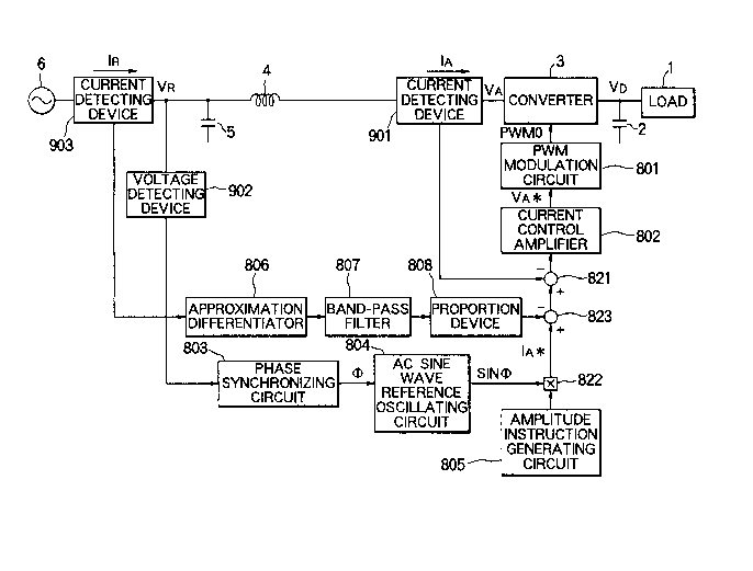
For example, Fig. 9 shows the block connection diagram
of conventional converter control circuit illustrated in High
Performance and Long Life Uninterruptable Power Source Using
Flywheel Energy Storage Unit, pp 1049 - 1055 in a bulletin of
IEEE Industry Applications Society Annual Meeting
(Oct. 7 - 12, 1990, Seattle).
Referring to Fig. 9, reference numeral 1 designates a
load, numeral 2 designates a capacitor which smooths a DC
voltage to be supplied to the load l, and numeral 3
designates a converter main circuit. The converter main
circuit has a single-phase full-bridge structure equipped
with switching elements Sl - S4, as shown in Fig. lOa, in
order to perform pulse-width modulation using triangular-wave
carrier of 1 - 2 KHz or more. Numerals 4 and 5 designate a
reactor for a filter and a capacitor, respectively, which are
provided between an AC power supply 6 and the aforementioned
converter 3. Numeral 901 designates a current detecting
device which detects converter current IA and numeral 902
designates a voltage detecting device which detects input
voltage VR.
In Fig. 9, numerals 800s designate the components of
2127516
the control apparatus of the aforementioned converter 3.
Numeral 801 designates a pulse-width modulating circuit
(hereinafter referred to as PWM modulating circui-t) which
transmits control output PWM0 for pulse-width-modulation for
controlling the aforementioned converter 3 according to the
converter voltage instruction VA * . Numeral 802 designates a
current control amplifier which obtains the converter voltage
instruction VA* to be supplied to the aforementioned PWM
modulating circuit 801 according to the output of a subtractor
821 which will be described later. Numeral 803 designates a
phase synchronizing circuit for obtaining the phase ~ of the AC
input VR according to a voltage detected by a voltage detecting
device 902.
Numeral 804 designates an AC sine wave reference
oscillating circuit for obtaining an AC sine wave reference
signal sin ~ having the same phase as the input voltage VR of
the AC power supply. Numeral 805 designates an amplitude
instruction generating circuit for sending an amplitude
instruction. Numeral 821 is a subtractor for obtaining
differences between a converter current instruction IA * obtained
by a multiplier 822 which multiplies the AC sine wave reference
signal sin ~ sent from the aforementioned AC sine wave reference
oscillating circuit 804 with an amplitude instruction sent from
the aforementioned amplitude instruction generating circuit 805
and the converter current IA detected by the current detecting
device 901 in order to transmit a signal representing such
difference to the aforementioned current control amplifier 802.
These components construct a current control loop.
The operation of the construction described above will
be described below.
2127516
The input voltage VR from the AC power supply 6 is
detected by means of the voltage detecting device and the phase
of the input voltage VR is detected by means of ~he phase
synchronizing circuit 803. The detected phase is input to the
AC sine wave reference oscillating circuit 804 in order to
obtain an AC sine wave reference signal sin ~ having the same
phase as the input voltage VR. The multiplier 822 multiplies
the output of the amplitude instruction generating circuit 805
and the output of the aforementioned AC sine wave reference
oscillating circuit 804 in order to obtain the converter current
instruction IA * .
The current control amplifier` 802 and the ~WM
modulating circuit 801 control switching action of the converter
3 to ma~e the converter current instruction IA * agree with the
converter current IA detected by the current detecting device
901, thereby forming a current control loop. Thus, under normal
conditions, power can be supplied to the load 1 from the AC
power supply ~ in the form of a sine wave current having a power
factor of 1.
The control apparatuses of power converters of the
prior art have the construction described above. For this
reason, if there is even a slight distortion in input voltage,
resonance is produced by the reactance component of this system
and the filter capacitor 5. This is a problem of the prior art
which must be solved. ~urther, if the control apparatus is
stopped when power is being supplied to the load 1, energy
stored in the reactance component of the system or energy stored
in the reactor for filter 4 flow into the filter capacitor 5
causing the capacitor 5 is charged with excess voltage. This is
another problem to be solved.
2127S16
-
The present invention provides a control apparatus for a
power converter, the control apparatus being capable of
restraining a resonance from being produced by the reactance
component of the system and the filter capacitor. The
S present invention also provides a control apparatus for a
power converter, the control apparatus being capable of
restraining excess voltage in a capacitor when the apparatus
is stopped.
According to the first aspect of the present invention,
there is provided a power converter control apparatus for
controlling a power converter comprising; a filter which
includes a reactor and a capacitor which are provided between
an AC power supply and the power converter; a resonance
detecting means which detects a resonance component caused by
the system reactor component existing between the AC power
supply and the capacitor of the filter and the capacitor of
the filter; a converter current detecting device which
detects a converter current flowing into the power converter
through the filter; an input voltage detecting device which
detects an input voltage supplied from the AC power supply; a
current instruction value generating means which obtains a
current instruction value for the power converter according
to the voltage detected by the voltage detecting device and
an amplitude instruction; a current instruction value control
means which changes the current instruction value output from
the current instruction value generating means according to a
resonance component detected by
2127516
the resonance detecting means; and a current control means which
obtains a voltage instruction value according to the difference
between the current instruction value output from the current
instruction value control means and a current value detected by
the converter current detecting device and then controls
switching elements of the power converter according to the
voltage instruction value.
According to the second aspect of the present
invention, there is provided a power converter control appar~tus
for controlling a power converter comprising; a filter which
includes a reactor and a capacitor provided between an AC power
supply and the power converter; a converter current detecting
device which detects a converter current flowing into the power
converter through the filter; an input voltage detecting device
which detects an input voltage supplied from the AC power
supply; a current instruction value generating means which
obtains a current instruction value for the power converter
according to a voltage detected by the voltage detecting device
and an amplitude instruction; a current control means which
obtains a voltage instruction value according to the difference
between a current instruction value output from the current
instruction value generating means and a current value detected
by the converter current detecting device and then controls
switching elements of the power converter according to the
voltage instruction value; and a stop announcement circuit which
outputs a stop announcement signal to the current instruction
value generating means before the apparatus is stopped and
controls the current instruction value for the power converter
so as to change the value to zero.
According to the third aspect of the present
~ ~U ~.~ ~ ~ 2~ b~ ~ 7 i~v~ z~ ~ r~ -~ ;; ~ r - p ~ h~ .~ ~ ~.~ ~-.~. .
2127516
_
invention, there is provided a power converter control apparatus
for controlling a power converter comprising; a filter which
includes a reactor and a capacitor provided between an-AC power
supply and the power converter; a resonance detecting reactor
which is provided between the AC power supply and the filter; an
input current detecting device which detects input current
flowing into the filter through the resonance detecting reactor;
a capacitor voltage detecting device which detects the capacitor
voltage of the filter; a converter current detecting device
which detects converter current flowing into the power converter
through the filter; an input current control means which obtains
the input current instruction value according to the detected
voltage by the input voltage detecting device and the amplitude
instruction and then obtains an output in which the current
value detected by the input current detecting device is
subtracted from the input current instruction value in order to
control the input current; a capacitor voltage control means
which obtains a capacitor voltage instruction value according to
the output of the input current control means and then obtains
an output in which the voltage value detected by the capacitor
voltage detecting device is subtracted from the capacitor
voltage instruction value in order to control the capacitor
voltage; a current control means which obtains a converter
current instruction value according to the output of the
capacitor voltage control means and then controls switching
elements of the power converter according to the output in which
the current value detected by the converter current detecting
device is subtracted from the converter current value in order
to control the converter current; and further, a stop
announcement circuit which outputs a stop announcement signal to
2127516
-
the input current control means before the apparatus is
stopped and controls the current instruction value for the
power converter so as to change the value to zero.
The invention will be described in more detail by
reference to the accompanying drawings, in which:
Fig. 1 is a block diagram showing the control apparatus
for a power converter according to the first embodiment of
the present invention,
Fig. 2 is a diagram of an equivalent circuit in which
the converter 3 and the reactor 4 shown in Fig. 1 are
replaced with a power source,
Figs. 3 - 8 are block diagrams showing the control
apparatus for a power converter according to the second -
seventh embodiments of the present invention, respectively,
Fig. 9 is a diagram showing the conventional control
apparatus for a power converter, and
Fig. lOa and lOb are circuit diagrams showing an example
of the construction of a power converter.
The first embodiment of the present invention will be
described below. Fig. 1 is a construction drawing showing
the control apparatus for a power converter according to the
first embodiment. In Fig. 1, the same reference numerals as
in an example of the prior art shown ln Fig. 9 designate the
same components. In Fig. 1, reference numeral 1 designates a
load, numeral 2 designates a capacitor which smooths a DC
voltage to be supplied to the load 1, and numeral 3
designates a converter
2127516
main circuit. Numerals 4 and 5 designate a reactor for a filter
and a capacitor, respectively, which are provided between an AC
power supply 6 and the aforementioned converter 3. N~meral 901
designates a current detecting device which detects converter
current IA and numeral 902 designates a voltage detecting device
which detects input voltage Va.
In the same Figure, the 800s numerals indicate the
components of the control apparatus of the aforementioned
converter 3. Numeral 801 designates a PWM modulating circuit
which transmits control output PWM0 for pulse-width-modulation
for controlling the aforementioned converter 3 according to the
converter voltage instruction VA *. Numeral 802 designates a
current control amplifier which obtains the converter voltage
instruction VA* to be supplied to the aforementioned PWM
modulating circuit 801 according to the output of a subtractor
821 which will be described later, in order to control the
converter current. Numeral 803 designates a phase synchronizing
circuit for obtaining the phase ~ of the AC input VR according
to a voltage detected by a voltage detecting device 902.
Numeral 804 designates an AC sine wave reference
oscillating circuit for obtaining an AC sine wave reference
signal sin ~ having the same phase as the input voltage ~V-R Of
the AC power supply. Numeral 805 designates an amplitude
instruction generating circuit for sending an amplitude
instruction. Numeral 821 is a subtractor for obtaining
differences between a converter current instruction IA * obtained
by a multiplier 822 which multiplies the AC sine wave reference
signal sin ~ sent from the aforementioned AC sine wave reference
oscillating circuit 804 with an amplitude instruction sent from
the aforementioned amplitude instruction generating circuit 805
2127516
and the converter current IA detected by the current detecting
device 901 in order to transmit a signal representing such
difference to the aforementioned current control amplifier 802.
These components construct a current control loop.
The construction of the present invention includes the
following novel components. Numeral 903 designates a current
detecting device which is provided between the AC power supply 6
and a filter including the reactor 4 and the capacitor 5, and
which detects input current IR. As regards the components of
the control apparatus, numeral 806 designates an approximation
differentiator which differentiates the input current IR
detected by the aforementioned current detecting device 903 and
numeral 807 designates a band-pass filter which permits only the
resonance frequency band of the input current IR to pass
therethrough according to the output of the approximation
differentiator 806. The approximation differentiator 806 and
the band-pass filter 807 form a detecting means for detecting
resonance current component.
Numeral 808 designates a proportion device for
obtaining the output in which the output of the band-pass filter
807 is multiplied by the gain K. Numeral 823 designates a
subtractor for obtaining differences between the converter
current instruction IA * obtained by means of the aforementioned
multiplier 822 and the output of the aforementioned proportion
device 808. The subtractor 823 and the proportion device 808
form a control means for changing current instruction values
according to the resonance current component. The
aforementioned devices builds a current control loop for
changing current instructions to the converter 3 so as to make
the output of the subtractor 823 agree with the converter
- 2127516
current IA detected by the current detecting device 901 or
namely, according to the resonance component of the input
current IR. ~-
The operation of the first embodiment described abovewill be described below.
The input voltage VR supplied from the AC power supply
6 is detected by means of the voltage detecting device 902 and
the phase ~ of the input voltage VR is detected by means of the
phase synchronizing circuit 803. The detected phase ~ is input
to the AC sine wave reference oscillating circuit 804 in order
to obtain an AC sine wave reference signal sin ~ having the same
phase as the input voltage VR. Then, the multiplier 822
multiplies the output of the amplitude instruction generating
circuit 80~ by the output of the aforementioned AC sine wave
reference oscillating circuit 804 in order to obtain the
converter current instruction IA * .
On the other hand, the input current IR detected by
means of the current detecting device 903 is differentiated by
means of the approximation differentiator 806 and the band-pass
filter 807 detects only the resonance fre~uency component. The
detected output is multiplied by the gain K by means of the
proportion device 808. The output of the proportion device 808
is subtracted from the aforementioned converter current
instruction IA * by means of the subtractor 823. Further, the
current control amplifier 802 and the PWM modulating circuit 801
form a current control loop for controlling the switching
elements of the converter 3 so as to make the output of the
subtractor 823 agree with the converter current IA detected by
means of the current detecting device 901.
~ ere, for example, suppose that the converter 3 and
2127~16
the reactor 4 are replaced with a current source. Fig. 2 shows
the construction of this case. In Fig. 2, numeral 7 designates
a reactor (hereinafter referred to as reactance component 7 as
well) which indicates reactance components of the system ~and
numeral 8 designates a current source in which the
aforementioned converter 3 and the reactor 4 are replaced
therewith. Assuming that the voltage of a capacitor 5, the
inductance of a reactor 7 of the system and the capacitance of a
capacitor 5 are Vc, L and C, respectively, the expressions (1),
(2) shown below are established if a transfer function is
considered.
L(dIR/dt) = VR - VC ( 1 )
C(dVc/dt) = IR + IA (2)
The input voltage VR can be obtained according to the
expressions (1), (2), as follows.
V~ = {LCS2 - L(IA/Vc)S + 1}Vc (3)
Where S is Laplace operator.
Referring to Fig. 1, the input current IR is
differentiated by means of the approximation differentiator 806
and the output from the approximation differentiator 806 passes
through the band-pass filter 807 and is then multiplied by the
gain K by means of the proportion device 808. Next, the output
from the proportion device 808 is subtracted from the converter
current instruction IA * by means of the subtractor 823. The
converter current IA flows so as to coincide with the output of
the subtractor 823. Thus, assuming that the transfer function
of the aforementioned band-pass filter 807 is f(S), the
converter current IA is obtained according to the expression (4)
shown below.
IA = KIRSf (S) = (K/L) (VR - VC ) f(S) (4)
2I 27S1 6
`_
If the expression t3) is substituted for the
expression (4), the input voltage VR is as follows;
VR = {LCS2 - K (VR /VC ) f(S)S + Kf(S)S + 1}Vc -~)
The aforementioned band-pass filter 807 allows only
the resonance current component to pass therethrough. In the
frequency band of the resonance current component, the transfer
function f(S) = 1. In the other frequency band, f(S) = 0.
Thus, the expression (5) can be expressed as follows.
In the resonance frequency band, the following
expression is established.
VC /VR = ( 1 + KS)/(LCS2 + KS + 1) (6)
In the other frequency band, the following expression
is established.
VC /VR = 1 + (LCS2 + 1 ) (7)
Thus, in the resonance frequency band, the power is damped by a
selected K value according to the expression (~), thereby
restraining resonance from occurring.
Thus, in the control apparatus of the power converter
3 according to the first embodiment described above, the current
control loop controls the switching elements of the converter 3
depending upon differences between the value of current flowing
to the converter 3 through the filter and the current
instruction value so as to make the aforementioned current value
agree with the current instruction value. Lecause the current
instruction value of the converter is changed according to the
resonance current component of the input current in this current
control loop, it is possible to restrain the LC resonance.
Fig. 3 is a construction diagram showing the control
apparatus for a power converter according to the second
embodiment. In Fig. 3, the same reference numerals as in the
-12-
2127516
first embodiment shown in Fig. 1 indicate the same components.
Thus, the description thereof is omitted here. In the second
embodiment, the points different from in the first Pmbodiment
are that instead of the current detecting device 903, a current
detecting device 905 which detects current flowing into a
capacitor 5 which constructs a filter is provided. Capacitor
curren* I~ detected by the current detecting device 905 is input
into a differentiator 806 to detect a resonance current
component. The current instruction value is changed according
to the resonance current component. The other components are
the same as in the first embodiment.
Next, the operation of the second embodiment will be
described below. In Fig. 3, a resonance current is generated
between a reactance component 7 of the system and the capacitor
5 of the filter and the current flows into the capacitor 5.
Thus, by detecting the capacitor current Ic, it is possible to
control the resonance which occurs between the reactance
component 7 of the system and the capacitor 5 of the filter.
Thus, the capacitor current Ic is detected by the current
detecting device 905 and the detected current is differentiated
~y the approximation differentiator 806. The band-pass filter
807 detects only the resonance frequency component and the
proportion device 808 multiplies the resonance frequency
component by the gain K. The output of the proportion device
808 is subtracted from the converter current instruction IA * by
means of the subtractor 823.
A current instruction obtained by the subtractor 823
is input into the subtractor 821. In a current control loop,
the current control amplifier 802 and the PWM modulating circuit
801 control the switching of switching elements of the converter
-13-
- 2127~16
3 so as to make the output of the subtractor 823 agree with the
converter current IA detected by the current detecting device
90 1 .
Thus, the construction according to the second
embodiment makes it possible to control the resonance which
occurs between the reactance component 7 in the system and the
capacitor 5 of the filter by detecting the capacitor current Ic.
Thus, it is possible to reduce the rating of the current
detecting device 905 to a smaller value than in the first
embodiment in which the resonance caused between the reactance
component 7 of the system and the capacitor 5 of the filter is
controlled by detecting the input current IR. For this reason,
the second embodiment has an effect of reducing operating cost
as well as the effect of the first embodiment.
Fig. 4 is a construction diagram showing the control
apparatus for a power converter according to the third
embodiment. In Fig. 4, the same reference numerals as in the
first embodiment shown in Fig. 1 indicate the same components.
Thus, the description thereof is omitted here. In the third
embodiment, the points different from in the first embodiment
are that; a reactor 9 is provided between the AC power supply 6
and the filter; a voltage detecting device 904 for detecting the
capacitor voltage Vc is provided; a subtractor 827 which inputs
the output obtained by subtracting the capacitor voltage Vc
detected by the aforementioned voltage detecting device 904 from
the input voltage VR detected by the voltage detecting device
902 into the band-pass filter 807 is provided, the approximation
differentiator 806 is eliminated and the current detecting
device 903 for detecting the input current I~ is eliminated.
The other components are the same as in the first embodiment.
-14-
- 2127S16
Usually, because the reactance component 7 of the
system is often unknown, it is not possible to specify a
resonance frequency. Thus, according to the construction shown
in Fig. 4, a reactor 9 which has a sufficiently larger capacity
than the reactance component in the system is added to the
apparatus and then a voltage VL applied to the reactor 9 is
obtained by subtracting the capacitor voltage Vc detected by the
voltage detecting device 904 from the input voltage VR detected
by the voltage detecting device 902 by means of the subtractor
827. Because the VL applied to the reactor 9 is differentiated
input current IR, it is possible to obtain the differentiated
value of the input current IR without using the approximation
differentiator utilized in the first embodiment.
The band-pass filter 807 detects only the resonance
frequency component from the output of the subtractor 827 and
the proportion device 808 multiplies the detected component by
the gain K. Then, the output of the proportion device 808 is
subtracted from the converter current instruction IA * by means
of the subtractor 823. The current control amplifier 802 and
the PWM modulating circuit 801 form a current control loop in
which the switching of the converter 3 is controlled so as to
make the output of the substractor 823 agree with the converter
current IA detected by means of the current detecting device
901 .
Thus, the construction according to the third
embodiment makes it possible to limit the resonance frequency by
adding the reactor 9 between the AC power supply and the filter.
Further, the necessity of the approximation differentiator is
eliminated by obtaining the voltage VL applied to the reactor 9,
thereby facilitating designing of the resonance control system.
2127516
`_
Namely, because the resonance component is detected according to
the reactor voltage and the converter current instruction is
changed depending on the resonance component, the present
embodiment has an effect of being capable of building up the
control apparatus easily as well as the effect of the first
embodiment.
Fig. 5 is a construction diagram showing the control
apparatus for a power converter according to the fourth
embodiment. In Fig. 5, the same reference numerals as in the
first embodiment shown in Fig. 1 indicate the same components.
Referring to Fig. 5, reference numeral 1 designates a load,
numeral 2 designates a capacitor for smoothing DC voltage to be
supplied to the load 1, and numeral 3 designates a converter
main circuit. Numerals 4, 5 designate a reactor for a filter
and a capacitor, respectively, which are provided between the AC
power supply 6 and the aforementioned converter 3. Numeral 901
designates a current detecting device for detecting a converter
current IA and numeral 902 designates a voltage detecting device
for detecting an input voltage VR.
In the same Figure, the 800s numerals indicate the
components of the control apparatus of the aforementioned
converter 3. Numeral 801 designates a PWM modulating circuit
which transmits the control output PWM0 for pulse-width-
modulation for controlling the aforementioned converter 3
according to the converter voltage instruction VA * . Numeral 802
designates a current control amplifier which obtains the
converter voltage instruction VA * to be supplied to the
aforementioned PWM modulating circuit 801 according to the
output of a subtractor 821 which will be described later, in
order to control the converter current. Numeral 803 designates
-16-
2127516
a phase synchronizing circuit for obtaining the phase ~ of the
AC input VR according to a voltage detected by a voltage
detecting device 902.
Numeral 804 designates an AC sine wave reference
oscillating circuit for obtaining an AC sine wave reference
signal sin ~ having the same phase as the input voltage VR of
the AC power supply. Numeral 805 designates an amplitude
instruction generating circuit for sending an amplitude
instruction. Numeral 821 is a subtractor for obtaining
differences between a converter current instruction IA * obtained
by a multiplier 822 which multiplies the AC sine wave reference
signal sin ~ sent from the aforementioned AC sine wave reference
oscillating circuit 804 by an amplitude instruction sent from
the aforementioned amplitude instruction generating circuit 805
and the converter current I~ detected by the current detecting
device 901 in order to transmit a signal representing such
difference to the aforementioned current control amplifier 802.
These components construct a current control 1Oop~
The construction of the present invention includes the
following novel components. Numeral 815 designates a stop
announcement circuit which transmits a stop announcement signal
to an amplitude instruction generating circuit 805 before the
control apparatus stops to zero the converter current and which
stops the control apparatus in order to prevent the capacitor 5
from being loaded with excess voltage after the converter 3
absorbs energy stored in the reactance component 7 in the system
and energy stored in the reactor 4 of the filter.
The operation of the fourth embodiment described above
will be described below.
The input voltage V~ supplied from the AC power supply
2127516
6 is detected by means of the voltage detecting device 902 and
the phase of the input voltage VR is detected by means of the
phase synchronizing circuit 803. The detected phase ~_is input
to the AC sine wave reference oscillating circuit 804 to obtain
an AC sine wave reference signal sin ~ having the same phase as
the input voltage VR. Then, the multiplier 822 multiplies the
output of the amplitude instruction generating circuit 805 by
the output of the aforementioned AC sine wave reference
oscillating circuit 804 to obtain the converter current
instruction I A * .
The current control amplifier 802 and the PWM
modulating circuit 801 form a current control loop which
controls switching of the converter 3 so as to make the
converter current instruction I A * agree with the converter
current I A detected by means of the current detecting device
901. Thus, under normal conditions, power can be supplied to
the load 1 from the AC power supply 6 in the form of a sine wave
current having a power factor of 1.
When the control apparatus is stopped during supplying
of power to the load 1, the stop announcement circuit 815
outputs a stop announcement signal to an amplitude instruction
generating circuit 805 before the apparatus is stopped.
Consequently, the amplitude instruction generating circuit 805
outputs zero. When the output of the amplitude instruction
generating circuit 805 becomes zero, the converter current
instruction I~* becomes zero. As a result, the converter
current I~ becomes zero and then the control apparatus is
stopped.
When the apparatus is stopped after the converter
current I A is zeroed, the converter 3 absorbs energy stored in
-18-
2127516
_
the reactance component 7 in the system and energy stored in the
reactor 4 of the filter during supplying of power to the load 1
before the apparatus is stopped. Namely, the control_apparatus
is stopped after the converter 3 absorbs energy stored in -the
reactance component 7 in the system and energy stored in the
reactor 4 of the filter. Consequently, the energies do not flow
into the capacitor S, so that the capacitor 5 is not loaded with
excess voltage.
Thus, according to the fourth embodiment, the stop
announcement circuit 815 transmits a stop announcement signal to
the amplitude instruction generating circuit 805 before the
apparatus is stopped. As a result, the apparatus is stopped
after the converter current becomes zero and then the converter
absorbs energy stored in the reactance component 7 in the system
and energy stored in the reactor 4 of the filter. Thus, the
present embodiment has an effect of preventing the capacitor 5
from being loaded with excess voltage.
Fig. 6 is a construction diagram showing the control
apparatus for a power converter according to the fifth
embodiment. In Fig. 6, the same reference numerals as in the
fourth embodiment shown in Fig. 5 indicate the same components.
Thus, the description thereof is omitted here. In the fifth
embodiment, the points different from in the fourth embodiment
are that a switch 10 for shutting the apparatus off from the
system, a switching detection circuit 810 for detecting whether
the switch 10 is open, a switch 811 which is turned on by the
output of the switching detection circuit 810 and an input
voltage instruction generating circuit 812 which generates an
input voltage instruction VR * are added to the system.
Further, the points of the fifth embodiment different
-19-
2127516
from the fourth embodiment are that a subtractor 825 which
subtracts a voltage detected by the voltage detecting device 902
from the input voltage instruction VR * input ~from the
aforementioned input voltage instruction generating circuit 8-12,
a voltage control amplifier 809 which outputs control current
according to the output of the aforementioned subtractor 825 in
order to control the input voltage and an adder 824 which adds
the output of the aforementioned voltage control amplifier 809
to the output of the multiplier 822 to input the result into the
subtractor 821 are added to the system.
Next, the operation of the control apparatus having
the construction described above will be described below.
~ eferring to Fig. 6, when the control apparatus is
stopped during supplying of power to the load 1, the stop
announcement circuit 815 outputs a stop announcement signal to
an amplitude instruction generating circuit 805 before the
apparatus is stopped. Consequently, the amplitude instruction
generating circuit 805 outputs zero and the converter current
instruction IA * becomes zero. As a result, the converter
current IA becomes zero and then the control apparatus is
stopped.
When the apparatus is stopped, the converter 3 absorbs
energy stored by the reactance component 7 in the system and
energy stored in the reactor 4 of the filter during supplying of
power to the load 1 before the apparatus is stopped. At this
time, because the capacitor 5 of the filter is connected to the
system, the system charges the capacitor 5.
When the switch 10 is open, the apparatus is separated
from the system and the switching detection circuit 810 detects
that the switch 10 is open. Consequently, the switch 811 is
-20-
2127~16
turned on by the output of the switching detection circuit 810.
When the switch 811 is turned on, the voltage control amplifier
809 is controlled so as to make the input voltage i~;truction
VR* from the input voltage instruction generating circuit -812
agree with the input voltage VR detected by the voltage
detecting device 902. Then, the output of the aforementioned
voltage control amplifier 8û9 is added to a converter current
instruction IA* output from the multiplier 822 by means of the
adder 824 to obtain a new converter current instruction.
The current control amplifier 802 and the PWM
modulating circuit 801 form a current control loop which
controls the switching operation of the converter 3 according to
the output of the subtractor 821 so as to make this new
converter current instruction agree with the converter current
IA detected by the current detecting device 901. Thus, a
voltage applied to the capacitor 5 is controlled to prevent the
capacitor 5 from being loaded with excess voltage.
Thus, according to the fifth embodiment, before the
apparatus is stopped, the stop announcement circuit 815
transmits a stop announcement signal to the amplitude
instruction generating circuit 805 to zero the converter
current. After this action, the voltage applied to the
capacitor S is controlled. As a result, the present embodiment
has an effect of preventing the capacitor 5 from being loaded
with excess voltage.
Fig. 7 is a construction diagram showing the control
apparatus for a power converter according to the sixth
embodiment. In Fig. 7, the same reference numerals as in the
fifth embodiment shown in Fig. 6 indicate the same components.
Thus, the description thereof is omitted here. The points of
- 2127S16
the sixth embodiment different from the fifth embodiment are
that a current control amplifier 813 for obtaining the input
voltage instruction VR * according to the output _from the
aforementioned subtractor 826 in order to control the in-put
current, an input current instruction generating circuit 814
which generates the input current instruction IR * for zero
current, and a subtractor 826 which subtracts the input current
IR detected by the current detecting device 903 from the input
current instruction IR * sent from the input current instruction
generating circuit 814 are added to the system. Further, the
points of the present embodiment different from the fifth
embodiment are that the switch 10 and the switching detection
circuit 810 are eliminated and that the switch 811 which is
turned on according to a stop announcement signal of the stop
announcement circuit 815 is added to the system. The other
construction is the same as in the fifth em~odiment.
Next, the operation of the apparatus having the
construction described above will be described below.
Referring to Fig. 7, the switch 811 is turned on
according to a stop announcement signal sent from the stop
announcement circuit 815 before the apparatus is stopped. When
the switch 811 is turned on, the current control amplifier 813
controls power so as to make the input current instruction IR *
sent from the input current instruction generating circuit 814
which outputs zero current instructions agree with the input
current I~ detected by means of the current detecting device
903.
Then, the subtractor 825 su~tracts the input voltage
of the voltage detecting device 902 from the output of the
current control amplifier 813 and according to the output, the
-22-
~127516
voltage control amplifier 809 transmits control current to the
adder 824. The adder 824 adds the output of the aforementioned
voltage control amplifier 809 to the converter_ current
instruction IA * output from the multiplier 822 in order-to
obtain a new converter current instruction.
The current control amplifier 802 and the PWM
modulating circuit 801 form a current control loop which
controls the switching of the converter 3 according to the
output of the subtractor 821 so as to ma~e this new converter
current instruction agree with the converter current IA detected
by the current detecting device 901. According to this system,
the apparatus is stopped after the input current IR is zeroed.
Thus, even if the apparatus is not separated from the system,
the capacitor 5 is not charged from the system. When the
apparatus is stopped, the capacitor 5 is not loaded with excess
voltage.
Thus, according to the sixth embodiment described
above, before the apparatus is stopped, the stop announcement
circuit 815 transmits a stop announcement signal to zero the
input current, thereby stopping the apparatus. Even if the
apparatus is not separated from the system, the capacitor 5 is
not charged. When the apparatus is stopped, the capacitor 5 is
not loaded with excess voltage.
Fig. 8 is a construction drawing showing the control
apparatus for a power converter according to the seventh
embodiment. In Fig. 8, reference numeral 1 designates a load,
numeral 2 designates a capacitor which smooths a DC voltage to
be supplied to the load 1, and numeral 3 designates a converter
main circuit. Numerals 4 and 5 designate a reactor for a filter
and a capacitor, respectively, which are provided between an AC
-23-
- 2127516
power supply 6 and the aforementioned converter 3. Numeral 901
designates a current detecting device which detects the
converter current IA and numeral 902 designates a voltage
detecting device which detects the input voltage VR_ Numeral
903 designates a current detecting device which is provided
between the AC power supply 6 and the filter built by a reactor
4 and a capacitor 5 in order to detect the input current IR and
numeral 904 designates a voltage detecting device which detects
a capacitor voltage of the filter.
In the same Figure, the 800s numerals indicate the
components of the control apparatus of the aforementioned
converter 3. Numeral 801 designates a PWM modulating circuit
which transmits control output PWM0 for pulse-width-modulation
for controlling the aforementioned converter 3 according to the
converter voltage instruction VA * . Numeral 802 designates a
current control amplifier which obtains the converter voltage
instruction VA * to be supplied to the aforementioned PWM
modulating circuit 801 according to the output of a subtractor
821 which will be described later, in order to control the
converter current. Numeral 803 designates a phase synchronizing
circuit for obtaining the phase ~ f the AC input VR according to
a voltage detected by a voltage detecting device 902.
Numeral 804 designates an AC sine wave reference
oscillating circuit for obtaining an AC sine wave reference
signal sin ~ having the same phase as the input voltage VR of
the AC power supply. Numeral 805 designates an amplitude
instruction generating circuit for sending an amplitude
instruction, the circuit transmitting zero output when a stop
announcement signal is transmitted from a stop announcement
circuit 815 which will be described later. Numeral 809
-24-
2127516
designates a voltage control amplifier which outputs the
converter current instruction IA * according to the output of the
subtractor described later in order to control the _capacitor
voltage VC. Numeral 813 designates a current control amplifier
which obtains the capacitor voltage instruction Vc* according to
the output from the subtractor described later in order to
control the input current IR.
Numeral 815 designates a stop announcement circuit
which transmits a stop announcement signal to the amplitude
instruction generating circuit 805 before the apparatus is
stopped, in order to zero the input current instruction IR * .
Consequently, when the apparatus is stopped, the capacitor 5 is
prevented from being loaded with excess voltage. Numeral 821
designates a subtractor which obtains differences between the
converter current instruction IA * obtained by the aforementioned
current control amplifier 809 and the converter current IA
detected by the current detecting device 901 to send a signal
representing such difference to the aforementioned current
control amplifier 802.
Numeral 822 designates a multiplier for obtaining the
input current instruction IR * by multiplying an AC sine wave
reference signal sin ~ sent from the AC sine wave reference
oscillating circuit 804 by an amplitude instruction sent from
the amplitude instruction generating circuit 805 in order to
obtain the input current instruction IR * . Numeral 825
designates a substractor which subtracts a voltage value
detected by the voltage detecting device 902 from a capacitor
voltage instruction Vc sent from the current control amplifier
813. Numeral 826 designates a subtractor which subtracts an
input current IR detected by the current detecting device 903
-25-
~127516
from the input current instruction IR sent from the multiplier
822.
Then, the operation of the apparatus according to the
seventh embodiment will be described below. Referring to Fig.
8, the control apparatus comprises a current minor loop which
controls a converter current IA, a voltage minor loop which
controls a capacitor voltage Vc and a current control loop which
controls an input current IR. The input voltage VR is detected
by means of the voltage detecting device 902 and the phase ~ of
the input voltage VR is detected by means of the phase detecting
circuit 803. The detected phase ~ is input to the AC sine wave
reference oscillating circuit 804. As a result, the AC sine
wave reference signal sin ~ having the same phase as that of the
voltage VR is obtained.
The multiplier 822 multiplies the output of the
aforementioned AC sine wave reference oscillating circuit 804 by
the output of the amplitude instruction generating circuit B05
and outputs the input current instruction IR * . The current
control amplifier 813 operates according to the output of the
subtractor 826 which obtains differences between the input
current instruction IR * which is the output of the
aforementioned multiplier 822 and the input current IR detected
by the current detecting device 901 and outputs the capacitor
voltage instruction Vc* so as to zero the difference, thereby
controlling the input current IR.
The capacitor voltage instruction Vc* which is the
output of the aforementioned current control amplifier 813 is
input to the subtractor 825. The subtractor 825 obtains a
difference between the capacitor voltage instruction Vc* and the
capacitor voltage Vc detected by the voltage detecting device
-26-
- 2127516
904. The output of the subtractor 825 is input to the voltage
control amplifier 809. The voltage control amplifier 809
outputs the converter current instruction IA * SO as tp zero the
difference between the capacitor voltage instruction Vc* which
is the output of the current control amplifier 813 and the
capacitor voltage Vc detected by the voltage detecting device
904, thereby controlling the capacitor voltage Vc.
The converter current instruction IA * which is the
output of the aforementioned voltage control amplifier 809 is
input to a subtractor 821. The subtractor 821 obtains a
difference between the converter current instruction IA * and the
converter current instruction IA detected by the current
detecting device 901. The output of the subtractor 821 is input
to the current control amplifier 802. The current control
amplifier 802 outputs the converter voltage instruction VA * SO
as to zero a difference between the converter current
instruction IA ~ which is the output of the voltage control
amplifier 809 and the converter current IA detected by the
current detecting device 901, thereby controlling the converter
current IA . Then, the converter voltage instruction VA * which
is the output of the current control amplifier 802 is supplied
to the PWM modulating circuit 801 and the output of the PWM
modulating circuit 801 controls the switching of the converter
3.
According to the seventh embodiment described above,
under normal conditions, power can be supplied to the load 1
from the AC power supply 6 in the form of a sine wave current
having a power factor of 1. The input current instruction IR *
is a sine wave and the current control amplifier 813 can respond
more quickly than the resonance frequency produced by the
-27-
- 2127516
reactor 9 and the capacitor 5. Thus, it is possible to control
the resonance produced by the reactor 9 and the capacitor 5.
When the control apparatus is stopped during supplying
of power to the load 1, the stop announcement circuit -815
outputs a stop announcement signal. When the stop announcement
circuit 815 outputs the stop announcement signal, the amplitude
instruction generating circuit 805 outputs ~ero. If the output
of the amplitude instruction generating circuit 805 becomes
zero, the input current instruction I~* becomes zero. If the
input current instruction IR * becomes zero, the input current IR
becomes zero, thereby stopping the apparatus. Because the
apparatus is stopped after the input current becomes zero, the
capacitor 5 is not charged from the system even if the apparatus
is not separated from the system. When the apparatus is
stopped, the capacitor 5 is not loaded with excess voltage.
According to the seventh embodiment described above,
the current instruction value of the current control loop which
controls current flowing through the converter 3 is changed
according to the resonance component produced by the reactor
component in the system and the capacitor 5 of the filter, and
the current flowing through the converter 3 is controlled to
zero before the apparatus is stopped. Thus, the present
embodiment makes it possible to prevent resonance and further
prevents the capacitor 5 of the filter from being loaded with
excess voltage when the apparatus is stopped.
The respective embodiments described above refer to a
converter 3 for a single phase. The embodiments are applicable
to three-phase full-bridge construction converter having the
switching elements S5 - S10 as shown in Fig. 10b.
The advantages of the respective embodiments will be
-28-
~ 2127516
described below. According to the first embodiment, the
converter current instruction is changed according to the
resonance component of input current, thereby restraining LC
resonance.
According to the second embodiment, the converter
current instruction is changed according to the resonance
component of the capacitor current. Thus, the second embodiment
has an effect of reducing operating cost as well as the effect
of the first embodiment.
According to the third embodiment, the converter
current is changed by the reactor voltage according to the
resonance component. Thus, in addition to the effect of the
first embodiment, it is possible to easily build up a control
circuit.
According to the fourth embodiment, by zeroing the
converter current before the apparatus is stopped, the converter
absorbs energy stored in the reactance component of the system
and energy stored in the reactor of the filter before the
apparatus is stopped. Thus, the capacitor is prevented from
being loaded with excess voltage.
According to the fifth embodiment, the apparatus is
separated from the system before the apparatus is stopped,
thereby controlling voltage applied to the capacitor. Thus, the
capacitor is prevented from being loaded with excess voltage.
According to the sixth embodiment, the input current
is zeroed before the apparatus is stopped. Thus, even if the
apparatus is not separated from the system, the capacitor is not
charged from the system. When the apparatus is stopped, the
capacitor is not loaded with excess voltage.
According to the seventh embodiment, by controlling
-29-
- 2127516
the input current, it is possible to build up the circuit in
addition to the effects of the third and sixth embodiments.
-30-