Note: Descriptions are shown in the official language in which they were submitted.
2127736
Packaging Structure For Microwave Circuit
Background of the Invention
The present invention relates to a packaging structure
for a microwave circuit, and more particularly to a
packaging structure including a microwave circuit module
or microwave IC module.
As well known, the wavelength of a microwave or
millimeter wave region is short and, therefore, it is
difficult to design a circuit arrangement including
transmission lines while suppressing discontinity on
the lines to a low level and ensuring isolation between
circuits or lines. Therefore, microwave circuit packaging
has necessarily been intricate and costly. In recent years,
a microwave monolithic integrated circuit (abbreviated
as MMIC hereinafter) is becoming gradually applied as a
semiconductor integrated circuits in the high frequency
band. However, the MMIC has many drawbacks. For example,
it is generally easy to crack so that many packaging
restrictions exist. In particular, it is not adapted
to integration of distributed constant circuits which
tend to result in large sizes.
Referring to Fig. 8 showing a packaging structure
for a conventional microwave circuit including an MMIC,
an MIC module 101 having a circuit element 103, microwave
leads 102 and bias supply terminals 107 therein are
2127736
arranged on a main plate 100. Here, the microwave leads
102 and the bias supply terminals 107 are led to the rear
side of the main plate 100 by going through outer conductive
holes 109 formed therein. The bias supply terminals 107
are soldered via a printed circuit board or the like, and
the microwave leads 102 are electrically connected to
another module or an isolator 108 by soldering via the
printed circuit board 104. The connected parts of the
microwave leads 102 are shielded by means of a cover 106
isolated from the outside.
As shown in Fig. 8, since the MMIC's are unsuitable
for integration of a distributed constant circuit
constituted mainly of passive elements, active elements
are sealed in an airtight case and connection between
these active elements and the outside passive elements
is established by microstrip lines and by soldering.
Therefore, the sealing of the MMIC into an airtight case
is costly, and an intricate and expensive shielding case
having finely compartmentalized small chambers is
required to prevent undesirable electrical connection
between unit circuits. Further, the cost for
assembling runs high.
Accordingly, the above-mentioned conventional packaging
structure has the following defects. (1) A considerable
cost has to be spent for building in an MMIC into an air-
tight case called a header. This is because the headeritself is expensive and the assembling cost is high also.
~ ~ ~7~3~
-- 3
(2) An intrlcate and large-slzed shieldlng case whlch ls
subdlvlded lnto small chambers is costly. (3) All of flxlng
of the header to the shleldlng case, flttlng of the prlnted
circult board, soldering of the termlnals, or the llke, have
to be done manually whlch result ln a hlgh assembly cost. (4)
The structure has a large slze and a large welght, and lt has
been a hlndrance to mlnlaturlzatlon and reductlon ln welght of
communlcatlon equlpment.
Summary of the Inventlon
It is therefore an ob~ect of the lnventlon to
provlde a packaglng structure for a mlcrowave clrcult havlng a
small-slze and low cost. It ls another ob~ect of the
lnventlon to provlde a packaglng structure for a mlcrowave
clrcult having excellent heat radlatlon efflclency. It ls a
further ob~ect of the lnvention to provlde a packaglng
structure for a mlcrowave circult, whlch ls exchangeable by a
circult module unlt. It ls a further ob~ect of the lnventlon
to provlde a package mlcrowave clrcuit uslng the
aforementloned packaglng structure.
Accordlng to the present lnventlon, there ls
provlded a packaglng structure for a mlcrowave clrcult
comprlslng a clrcult module havlng a semlconductor element; a
mother substrate accommodatlng sald clrcult module thereon;
thermal spreadlng means mounted on sald clrcuit module for
recelvlng heat from said clrcult module; radlatlng means
recelvlng heat from sald thermal spreadlng means for radlatlng
sald heat; a heat conductive elastomer dlsposed between sald
thermal spreadlng means and sald radlating means; and means
66446-588 -
7 3 ~
-- 4
for pressing said mother substrate in the directlon of said
radiating means, whereln sald clrcult module lncludes: a
multllayered substrate accommodating said semiconductor
element thereon, said multilayered substrate havlng two flrst
grounding conductive layers and a first center conductive
layer between said two first grounding conductive layers, said
first center conductive layer having a first connecting line
pattern, a first center conductive via for leading said first
connecting line pattern to a surface of sald clrcult module,
and a plurality of first groundlng conductive vlas connecting
said two first grounding conductive layers, said plurality of
first groundlng conductlve vlas belng arranged around sald
flrst center conductive vla and around sald semlconductor
element.
BRIEF DESCRIPTION OF THE DRAWINGS
Fig. 1 shows a sectional vlew of a packing first
embodlment according to the invention;
Figs. 2(A) and 2~B) show electrode arrangements on a
mother substrate and on a clrcuit module, respectlvely, in the
embodlment shown in Fig. l;
Flg. 3(A) is a sectlonal vlew of a package mlcrowave
clrcult devlce to which the packaging structure shown in Fig.
1 is applled;
Flg. 3(B) ls a partlal vlew of the spring assembly
shown in Fig. 3(A);
Flg. 4 ls a sectlonal vlew of another packaged
mlcrowave clrcuit devlce to whlch a second embodlment ls
applied;
66446-588
~ ~ ~7~
. ~ .
- 4a -
Flg. 5 ls a sectlonal vlew of a further packaged
mlcrowave clrcult devlce to whlch a thlrd embodlment ls
applled;
Flg. 6 shows a sectlonal vlew of a packaglng
structure accordlng to a fourth embodlment;
Flg. 7 show~ a sectlonal vlew of a package structure
66446-588
212~73fi
according to a fifth embodiment; and
Fig. 8 shows a conventional packaging structure of
a microwave circuit.
Description of Embodiments of the Invention
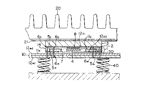
Referring to Fig. 1 showing a sectional view of the
packaging structure for a microwave circuit according to
a first embodiment of the invention, the description will
proceed from that about the structure of various parts to
that about the overall structure. In Fig. 1, a circuit
module 1 accommodates at least one semiconductor element
4 having microwave circuits in its internal space. The
circuit module 1 further has a multilayered structure 14
obtained by laminating dielectric layers and a conductor
layer. In the embodiment, the structure 14 includes a
center conductor layer llc, dielectric layers and a pair
grounding conductor layers 12Cl and 12C2 on the dielectric
layers. The two grounding conductor layers 12Cl and 12C2
are mutually connected by grounding conductor vias (inter-
layer connecting conductors) 6c. The grounding conductor
vias 6c are provided in large number in the periphery of
the circuit pattern formed on the center conductor where
the disposing interval of the vias 6c is designed to be
less than 1/8 of the wavelength corresponding to the
frequency processed in the circuit module 1. A signal
is led out to a surface of the circuit module 1 by means
. , , 2I27736
of the center conductor vias 5c~ and ls connected to a
surface electrode pattern having a bump 30 thereon. The
grounding conductor vias 6c are provlded so as to surround
the center conductor vla 5c~ and thelr tlps are connected
to grounding electrodes 6a (see Flg. 2) on the surface.
Heat conductlve vlas 8 are provlded to release heat
generated by the semlconductor element 4. The generated
heat runs off to a thermal spreading plate 3 through the
vias 8 having excellent heat conductivity. The heat
conductlve vlas 8 are made of Cu/W or Ag composltlon
material. The semiconductor element 4 is accommodated
in the space within the circuit module l, and ls shlelded
by a lid 7 made of a good electrlcal conductor. The
thermal spreadlng plate 3 is flxed by a bondlng materlal 2
to the circult module surface where the semlconductor
element 4 ls lnstalled.
Next, a mother substrate 10 wlll be descrlbed. The
mother substrate lO ls formed of a flexlble organlc materlal,
and lt ls posslble to constltute a larger scale clrcult unlt
by uslng a large-slzed substrate lO wlth a plurallty of
clrcuit modules l. The mother substrate 10 has at least
two grounding conductor layers 12ml and 12m2 and a center
conductor layer llm therebetween. In order to confine
a mlcrowave slgnal into the lnterlor of the substrate lO,
there are provided a large number of grounding conductor
vias 6m~ which connect with the upper and lower external
2127736
-- 7 --
conductors, in the periphery of the center conductor llm.
The grounding conductor vias 6m need be provided to surround
at least the circuit pattern of the center conductor llm
and ideally, it is to be provided allover the surface of
parts where the center conductor pattern is not found to
confine the microwave signal perfectly. In this way,
energy of the microwave signal is confined to the periphery
of the center conductor layer llm.
For the circuit module 1, analogous to the case of
the mother substrate 10, a large number of the grounding
conductor vias 6c connecting the grounding conductor
layers 12Cl and 12C2 are provided arround the circuit
pattern of the center conductor layer llC and, if possible,
the other allover part where the circuit pattern of the
center conductor layer llC does not exist.
Further, electrode arrangements of the mother
substrate 10 and the circuit module 1 will be described.
In Fig. 2(A) showing the electrode arrangement of the
mother substrate 10, the grounding conductor layer 12m2
has exceptional non-grounding conductive parts, i.e., the
electrodes 5a and 9a for an input/output signal and a DC
bias/low frequency signal, respectively. Further, the
allover surface except for grounding electrodes 6a and
the electrodes 5a and 9a is resisted. The electrodes 6a,
5a and 9a connect with the respective vias. As the same
as the vias 6m~ the grounding electrodes 6a are arranged
2127736
-- 8
not only around the electrodes 5a for the center conductor
layer but also in the periphery of the circuit module 1,
at least. In this figure, dot lines 11 and 13 indicate
the input/output signal lines and the bias/low frequency
signal lines, respectively. As shown in Fig. 2(B), the
surface of the circuit module 1 has grounding electrodes
6a and signal electrodes 5a and 9a, which connect with
the respective electrodes 6a, 5a and 9a on the mother
substrate 10 through the bumps 30 (Fig. 1). In this
connection, it is possible to provide the bump 30 on
the electrodes of the mother substrate 10 instead of
the provision on the electrodes of the circult module 1.
Accordingly, since the microwave signals are confined to
the interior of the circuit module 1 and the mother
substrate 10 as in the above, there is no need of
providing an intricate shielding case as is required in
the conventional microwave circuits, and it is possible
to realize a large-scale microwave circuit with a compact
structure. -
Next, cooling for the microwave circuit structure
according to this invention will be described. In Fig. 1,
heat generated from the semiconductor element 4 has to be
discharged effectively to the outside of the equipment.
A method which is generally employed for such a purpose
is to use radiating fins. Such radiating structure is
disclosed in, for example, Japanese Laid-open Patent
2127736
Applications No. 60-21611 (1985) and No. 60-64503 (1985).
However, it is impossible to apply this radiating structure
for a packaged microwave circuit device. Further, the
method is applicable only to a cooling system of external
air intake type, and cannot be applied to closed type
equipment. If a heat radiating plate is attached directly
to the thermal spreading plate, heat can be taken directly
to the outside through the thermal diffusion plate.
However, it is impossible to closely attach mechanically
a plurality of circuit modules to the heat spreading plate.
This is because it is difficult to make the top surface
of the thermal spreading plate flat with high precision
(to be on the same plane) for all of the circuit modules
due to difference in the size of soldering or the like.
Moreover, if the heat radiating plate is fixed to the
thermal spreading plate, then a stress is applied to
bonded electrode parts of the circuit module and the
mother substrate due to the difference between thermal
expansion coefficients of the mother substrate and the
heat radiating plate, causing damages to the bonded parts.
In this embodiment of the invention, a heat conductive
elastomer 21 is inserted between the thermal spreading
plate 3 and the heat radiating plate 20, and a pressure
is applied to the mother substrate 10 by means of a spring
40 so as to bring the thermal spreading plate 3 and the
heat conductive elastomer 21 to a close contact. With
2127736
- 10 -
this arrangement, even if there was unevenness in the
height of the top surface of the thermal spreading plate 3
with a plurality of circuit modules attached thereto, such
an unevenness can be absorbed by the heat conductive
elastomer 21. The heat conductive elastomer 21 is made
of silicon resin and AQN/ for example. Now, the thermal
conductivity of heat conductive elastomers is generally
not high compared with that of metals. Nevertheless, the
disadvantage that the conductivity of the heat conductive
elastomers is low will not cause a problem in practice
because of spreading of heat generated by the semiconductor
element to a broad area by means of the thermal diffusion
plate. Fig. 3 shows a packaged microwave circuit device
using the packaging structure of the invention. In this
figure, three circuit modules 1 are contained and radiating
plate 20 is directly formed on a device body. The body and
"~ a lid 51 compose of an airtight case 50. An input/output
signal and a DC source are applied or derived through a
connector 52. Numeral 53 indicates a connector terminal
connecting with a conductor line on the mother substrate 10
and numeral 54 an O ring. A plurality of springs 40 are
installed on the lid 51 through holders 51'. By assembling
the lid 51 to the body, the springs 40 press the mother
substrate 10 and, thus, the thermal spreading plate 3 is
pressed to the radiating plate through the heat conductive
elastomer 21. Therefore, heat generated from the circuit
2127736
-- 11
module 1 is efficiently discharged through the thermal
spreading plate 3, the heat conductive elastomer 21 and
the radiating plate 3, without any stress to the elements.
In this case, the connector terminal 53 has elasticity
and, therefore, the connection between the connector
terminal 53 and the conductor line becomes completed
when the springs 40 press the mother substrate 10.
The springs 40 may be provided one for each circuit
element, and may be added more as need arises. When the
circuit scale is small, the number of the springs 40 may
be decreased. Further, there is no restriction on the
type of the spring; it may be selected appropriately from
among a coil spring, leaf spring, plastic foam, or the
like, which can exert the pressure to the mother substrate.
Fig. 4 shows another packaged microwave circuit device
utilizing a plastic sponge form 55 having a spring function,
instead of the coil springs 40 in Fig. 3. The plastic
sponge form 55 has an advantage to equally provide pressure
to the mother substrate. Fig. 5 shows a further packaged
microwave circuit device utilizing a plurality of leaf
springs 57. Numeral 56 indicates a base plate. In this
case, it is possible and advantageous to produce the leaf
spring 57 together with the base plate 57 by plastic-molding.
Since the purpose of applying pressure is to bring the
thermal spreading plate in close contact with the heat
conductive elastomer, it is possible to apply the pressure
2I27736
- 12 -
by utilizing elasticity of the mother substrate, resulting
no-use of a spring. In that case, the structure can be
made simpler than in the case of providing spring means
separately, but there is required a rigorous design about
the deformation amount (warping) of the mother substrate.
The mother substrate is made of a organic material
such as a epoxy-glass plate since elastic characteristic
is essential to the mother substrate. In this connection,
the circuit module may be made of the organic material as
the same as the substrate. On the other hand, it is,
of course, possible to apply a ceramic material to produce
the circuit module. In the case applying the ceramic
material, it is necessary to consider a difference of
heat expansion between the organic material (mother
substrate) and the ceramic material (circuit module).
Since the heat expansion ratio is different between the
organic and ceramic materials, shearing stress due to
temperature change is applied to the bump and the bump
becomes distroyed if the stress is in excess of tolerance.
The tolerance is dependent on the size of the circuit
module. Therefore, when the size of the circuit module
is large and temperature is varied in a wide range, it
is preferable to inject a resin material between the
circuit module and the mother substrate to avoid that
the stress concentrates on the bump. Fig. 6 shows this
arrangement in which the resin 60 is provided.
21277~;
Various modifications to the packaging structures for
a microwave circuit according to the invention can be
thought of. When it is necessary to build an external
capacitor with large capacitance or a low frequency
semiconductor chip in the circuit module, these components
are installed on the surface of the circuit module according
to the surface packaging system. A packaging mode in that
case is shown in Fig. 7 as a fifth embodiment. The thermal
spreading plate 3 is limited only to the part of the surface
of the circuit module l which is in the rear of the part
where the semiconductor element 4 is installed, and a chip
active element 41 and chip passive elements 42 are installed
on the remaining parts of the surface. In this case, care
should be exercised as much as possible so as not to reduce
the area of the thermal spreading plate 3.
As described in the above, in the packaging structure
for a microwave circuit according to this invention,
microwave signals are confined into the interior of the
circuit module and the mother substrate, without a shielding
case which is intricate and large as well as expensive.
In addition, by constructing a whole circuit by the circuit
module which accommodates active elements consisting mainly
of a semiconductor integrated circuit, and the mother
substrate loaded with a plurality of the circuit modules,
whose main function is mutual connection or integration,
standardization of the circuit module as a unit became
2127736
- 14 -
possible, and improvement of reliability and cost reduction
are brought about by the mass production effect of the
modules. Moreover, yield is also enhanced since replacement
by the unit of module becomes feasible even when defective
circuit modules are found.
Furthermore, according to this invention, heat
generated by the semiconductor element accommodated in
the circuit module is dispersed by the thermal spreading
plate, and is let out by being directly transmitted to the
heat radiating plate of the device via the heat conductive
elastomer. Accordingly, the temperature of the semiconductor
element can be lowered and its life can be prolonged. Or,
conversely, it is possible to extract the highest available
output from the semiconductor element. For the case of
the mother substrate having a plurality of circuit modules
thereon, even when it is difficult to obtain perfect
flatness (identity of the plane) of the top surface of
the thermal spreading plate, resulting in the occurrence
of unevenness, the heat conductive elastomer absorbs
slight errors so that excellent thermal conduction can
be ensured.
As described in the above, the configuratlon of this
invention can be simplified to such an extreme extent that
it is possible to achieve a remarkable cost reduction
compared with the conventional packaging structure.