Note: Descriptions are shown in the official language in which they were submitted.
21283~7
PROCESS AND DEVICE FOR THE CONTROL OF A
MICROTIP FLUORESCENT DISPLAY
DESCRIPTION
TECHNICAL FIELD
The present invention relates to a process and a device for
the control of a matrix display for displaying images having .-
different grey levels, of the microtip fluorescent display
type. As the images can be in black and white or in colour,
in the latter case the term "grey level" stands for "colour
half-tones".
PRIOR~ART
Microtip fluorescent screens or displays are known and are in
partlcular descrlbed by R. Meyer in the article entitled
"Microtip Fluorescent Dlsplay" (Japan Dlsplay, 86, p 512).
It is known that for the control of the display of images on
a matrix display, use is generally made of a "one row at a
time" addressing principle. The addressing of a microtip
display having L rows and M columns consequently takes place
row by row (row time - TL) during a frame of duration TT
exceeding or equal to LxT . During the addressing of each
row, the informatlons to be dlsplayed on the M pixels of said
row are simultaneously applied to the M display columns.
An article by T. Leroux, A. Ghis, R. Meyer and D. Sarrasin
entitled "Microtips Display Addressing" (SID 91 Digest, pp .:
437 to 439) contains a description of the operating principle
of such displays, as well as the different ways of addressing
them. This article makes a distinction between two addres-
sing types: :
- an analog addressing consisting of sampling, after amplifi-
cation, an analog source signal and transferring to the ~:
B 11596.3 DB
2128357
.: `
column in question a voltage directly proportional to the
video signal,
- a digital addressing in Pulse Width Modulation (PWM) con- ~ -
sisting of switching a so-called on voltage for a time longer
or shorter than the row selection time TL, as a function of
the grey level to be displayed, as described in French patent
application FR-A-88 08756 of 29.6.1988.
There are also variants of solutions of the digital type.
Firstly there is a Prame Rate Control or FRC. This method is
in particular described in EP-A-384 403 and EP-A-364 307 in
the case of STN displays (multiplexed LCD's) and consists of
carrying out several scans of the image successively alloca-
ting on or off states to the same image elements, the eye
serving as the integrator. There is also a method using
multilevel clrcuits. This method consists of using circuits
able to switch N different voltage levels (in practice N=8 or
N=16). To each voltage corresponds a given grey level. This
method also uses eight level circuits on two frames, which
makes it possible to obtain with the same voltages and dura-
tions, sixteen grey levels, as described in the article by
H. Mano, T. Furuhashi and T. Tanaka entitled "Multicolor
Display Method for TFT-LCD" (SID 91 Digest, pp 547 to 550).
:: .
It is also possible to use eight level circuits on two succe-
ssive frames, but allocating a different significance to the
frames by means of voltages. The first frame e.g. supplying
the low orders (O, 1, 2, 3, 4, 5, 6, 7) and the second the
high orders (O, 8, 16, 24, 32, 40, 48, 56), which makes it
possible to obtain sixty four grey levels, as described in
the article by K. Takahara, T. Yamaguchi, M. Oda, H. Yamaguchi
and M. Okabe entitled "16-Level-Gray-Scale Driver Architecture -
and Full-Color Driving for TFT-LCD" (IDRC 91 Digest, pp 115
to 118). However, this method limits the screen contrast.
~ -`
Nowadays, in the world of flat screens, competition has been
.:
B 11596.3 DB
r-~ 2128357
-- 3
established around a few key points. One of them is a search
for low consumption levels. Two of the described addressing
variants for the display of grey levels are more interesting
from the screen capacitive consumption standpoint, namely the
S analog control and the method using multilevel circuits,
which is in practlce limited to sixteen voltage levels.
The practical performance of the analog control with circuits
functioning in linear form leads to a difficult compromise.
Thus, in such an operation, if the display has a very low
consumption, it is necessary to supply a non-negligible
current in order to polarize the output stage of the circuits.
In addition, the more it is wished to have short times for
passing from one level to another (corresponding to the
addressing of two successive rows) the more it is necessary
to increase said current and therefore the consumption of the
control electronics.
Digital circuits have the interest of a very low consumption,
because they function as switches, without requiring a polari-
zing current and wlth very short response times. The method
using multilevel circuits comes close to the ideal solution,
but if it is wished to display Q=256 grey tones, it is
clearly impossible to envisage a circuit having 256 voltage
inputs and the same number of 256 channel analog multiplexers
as outputs to be driven.
Another prior art document, namely EP-A-478 386 applies to
Thin Film Transistor or TFT displays. In the proposed con-
::
trol method, the aim is to obtain on the considered columncontrol electrode, at the end of the row selection time, a
column voltage determined by the data supplied by the source.
According to the prior art a voltage chosen from among N
external voltages is switched, said application proposing a
means for obtaining a large number of different final
B 11596.3 DB
2i283~7
- 4 -
voltages on the basis of a restricted number of external
voltage sources. The principle consists of charging the
column with the external voltage which is available and below
or equal to, but as close as possible to the desired flnal
value and then, when the first voltage is established and at
a time dependent on the desired final voltage (and therefore
the grey level to be displayed), the immediately higher,
available external voltage. As the passage to said voltage
takes place with a certain time constant linked with the cap-
acitance of the column and the access resistance to said
capacitance, the stored voltage on the capacitance being that
obtained at the end of the row time (Rq: in a TFT display,
each pixel is linked with a column electrode across a trans-
istor operating as a switch and which is driven by the row
electrode and at the end of the row time said switch is
opened, so that there is a high impedance passage to the
pixel capacitance and the storage of the voltage thereon).
By acting on the time of tripping the second voltage, at the
end of selection it is possible to obtain a complete series ~-
of intermediate voltages.
The invention aims at proposing a process and a device for
the control of a matrix display of the microtip fluorescent
display type ma~ing it possible to solve the different
problems referred to hereinbefore. -
. ~ . ': ' .
DESCRIPTION OF THE INVENTION
:,: , , -
The invention therefore relates to a process for the control
of a microtip fluorescent display formed from pixels arrangedin accordance with L rows and M columns of images which can
have a discreet number of Q grey tones, said process com-
prislng, at each selectlon of a row of the display durlng a
row selection time TL, the simultaneous application to the
display columns of voltages corresponding to the grey levels
. B 11596.3 DB -
2128357
. .
-- 5
to be displayed at the image points corresponding to the
intersection of said row and said columns, wherein the diff-
erent column voltage values applicable to the columns are
chosen in a strictly increasing sequence of N+l values such
that the row selection time is subdivided into S equal time
intervals ~t, each voltage value being applied an integral
number of time ~t, (NxS)+1 representing the number Q of grey
levels, with ~ >2 and S 22, and in that during the row selec-
tion TL and as a function of the grey level to be displayed
at an image point, the corresponding column voltage assumes
a first value Va for a certain number of time intervals ~t,
and then, if need be, during the remaining time intervals at
the most one second value Vb, said second value following on ~.
to the first in the sequence of N voltages.
In this process use is made of an addressing method having
both time and voltage modulation possibilities offered by the
electro-optical respQnse of microtip fluorescent displays.
Beyond the emission threshold, the brightness obtained is an
effect proportional to (VxT), V being the cathode gate volt-
age applied and T the duration of the application of said :~ :;
voltage. As a result of the present invention, there is a
combination of the advantages of the consumption of digital
circuits and the analog addressing method, whilst permitting :
the selection of a large number of grey levels.
The invention also relates to a device for controlling thecolumns of a microtip fluorescent display making it possible
to display grey levels comprising a digital data source
supplying words K encoding the information to be displayed
on k bits, a display controller receiving synchronization
signals from the data ~ource and controlling the different
signals able to drive the control circuits of the display
columns, a generator of (N+1) discreet voltages, the control
B 11596.3 DB
21283~7
-- 6
circuits for the display columns incorporating a shift
register with k inputs and k x ~ outputs, each output belng
associated with a storage flip-flop and analog multlplexing
means connected on the one hand to the k x M flip-flops and
to the generator and on the other to the M columns, said
means making it posslble to switch to each column a voltage
chosen from among N+l as a function of the word K stored ln
the k flip-flops associated with said column.
Each word K stored in the k flip-flops of a control circuit
of a column ls subdlvided into two words H and B such that
the word H is constituted by the h most significant bits of
K with 2h=N+1 and such that the word B is constituted by the
(k-h) remaining least signlflcant bits, the multiplexing ~-
means of the control clrcult of a column comprising a binary :
decoding circuit of n bits 1 from among 2 connected to the h
flip-flops of said column having in the memory the h most
signlflcant bits, sald circuit producing N signals Ho to
HN 1 translatlng the codlng of H and making it possible to
select the palr of column voltages (Vi, Vi+l) adapted to the
grey level to be dlsplayed, a comparator connected to the
(k-h) least slgnlflcant blts and wlth a sequencer able to
supply the addresslng sequence wlthln a row time coded on
(k-h) bits, - ~:
a combinatorial logic clrcuit connected to the outputs of the
decoding clrcuit and to the comparator, N+l analog switches,
whose analog lnputs are connected to the generator and the
valldatlon lnputs to the combinatorlal logic clrcuit and
whereof all the outputs are connected to the correspondlng
column.
The sequencer supplles the index P of the addressing sequence
wlthln a row tlme, sald lndex P belng coded on (k-h) blts.
Thls sequencer i8 advantageously a counter, whose clock has
2(k h) pulses per row tlme, sald counter belng inltlallzed
B 11596.3 DB
2128357
.
-- 7
for each row time. The comparator performs the comparlson
between the signals P and B and supplies a coding bit E such
that:
P< B=~ E = I
P >B==~E = 0.
The combinatorial logic circuit between the coding bit E and
the signals Ho to HN_1 makes it possible to obtain the sig-
nals Fo to FN driving the N+1 analog switches, such that:
Fo ~-Ho
F1 = E-Ho + E-H1
Fi = E.Hi_l + E-Hi
F~_1 = E HN_2 + ~-HN-1
FN ' E - HN -1 ~.
-
so as to position in time the voltage change Vi to Vi+1.
The generator of N+l discreet voltages can be constituted by
operational amplifiers connected as following amplifiers,
with input voltages fixed by a resistive divider bridge
(R1, R2, ..... RN). In the case of a linear distribution of
the voltages, the resistances all have the same value.
The generator of N+1 discreet voltages can also be based on
one or more digital-analog converters, which are themselves
driven by a controller responsible for calculating the values
of the N+1 voltages.
A black and white or colour palette circuit can also make it
possible to control the generator of discreet voltages in the
manner required by the user.
B 11596.3 DB
... .. ~ . . . . ..
~ 21283~7
BRIEF DESCRIPTION OF THE DRAWINGS
Fig. 1 shows an example of a signal for activating the
columns of a matrix display.
Fig. 2 shows the brightness/voltage response of a microtip
fluorescent display.
Figs. 3A and 3B show the distribution of the brightness as
a function of the voltage.
Figs. 4 and 5 illustrate the device according to the -
invention.
~ ,-
Figs. 6 and 7 illustrate embodiments of the circuit of the ~ ~
device according to the invention. -
DETAILED DESCRIPTION.OF EMBODIMENTS
i -
The invention relates to a process for the control of a micro-
tip fluorescent display formed from pixels arranged in accor~
dance with L rows and M columns of images which can have a
discreet number of grey tones.
In this process, the columns (cathodes) are controlled by the
signals used for activating them. These column signals per-
mit the selection of a voltage Vi from among N+l with
N ,2 and O ~i <N. These N+l voltages Vi are chosen such that
their values form a strictly increasing sequence. The row
time is subdivided into S equal time intervals ~t, S being an
integer with S22. This leads to a squaring or chequering of
the time-voltage space with ~SxN boxes or squares, each of
them representlng a brightness supply proportional to its
significance VxT.
.~ ,"
B 11596.3 DB
2~283~7
During a row selection time TL and as a function of the grey
level to be displayed, the column signal must assume a first
voltage value Va for a certain number of time intervals ~t
and then, if need be, during the remaining time intervals, at
the most one second voltage value Vb, which follows on to the
first in the sequence of N voltages. This second value must
be such that:
Vb = Va ~ ~V
If the order 1 grey tone is obtained by the application of a
voltage Vl for a time ~t, the order 2 grey tone will be -~
obtained by the application of the voltage V1 durlng a time
at ~ ~t, and for obtaining the order S grey tone it is neces~
sary to apply it for S times the time ~t. The order (S~1)
grey tone will be obtained by applying a voltage V2 for a
time ~t and the voltage V1 for the (S-1) other time inter-
vals.
Fig. 1 gives an example of a signal for activating the col-
umns of a matrix display in the case N=8 and S=8 making it
possible to generate N x S = 8 x 8 = 64 grey levels. The
signal corresponds to the display of grey No. 42, i.e. the
activation of squares 1 to 42 in the drawing. Compared with
a conventional control operating in multilevels, it is poss-
ible to obtain a large number of grey levels e.g. 256 withpairs ~N=16 and S=16~ or ~N=8 and S=32~, whilst having a
single supplementary transition between two ad~acent levels
(~V = VN/N in the particular case of a linear voltage
sequence), 80 that the consumption "cost" is at a minimum,
because the capacitive con~umption of a transition is propor-
tional to the square of the voltage shift ~V.
The N+1 voltages Vl can e.g. be such that for i from 0 to N:
Vi = ix(VN/N), which gives the same significance ~Vx ~t to
each shift between consecutive grey levels. However, it is
B 11596.3 DB
2128357
-- 10 -
advantageously possible to choose a non-linear distribution
by differently graduating the voltages, which makes it poss-
ible to adJust the electro-optical response of the display ln
accordance with the wishes of the user. Thus, the brightness/
voltage response (row/column or grid/cathode VGc) of a micro-
tip fluorescent display is in accordance with fig. 2, so that
by using equal time intervals and appropriately chosen vol-
tages, it is possible to bring about correspondence in succes-
sive ranges between said response and the desired curve.
In order to obtain a given sequence of brightness values, ~ -
it is possible to find a single sequence of voltages on the -
basis of a brightness/voltage response curve. Thus, it is~ -
possible to carry out a gamma correction for television~ ;
application or fulfil the function of a palette circuit for ~-
data processing-type applications. ~ ~-
Unlike in the case of~ the aforementioned EP-A-478 386, the
process according to the invention is applicable to the part-
icular case of microtip screens or displays. The electro-
optical response of said displays differs from that of active
matrix liquid crystal displays (TFT). Thus, for a TFT-type
display, for a row time charging takes place of a voltage,
which is then maintained on the pixel throughout a frame (com-
plete scan of the image), said voltage driving the switchingof the molecules and therefore the modulation of the light
transmitted durlng the complete frame. For a microtip dis-
play, the electro-optical response takes place immediately
during the row selection time and the considered pixel only
emits during this row time.
The voltage applied to a selected row brings the column/row
voltage to the limit of the emission threshold (whereas the
column/row voltage for an unselected row is still below said
threshold). Moreover, the voltage applied to a column during
B 11596.3 DB
21~83~7
11 --
this row selectlon time immediately brings about a more or
less pronounced emission (as a function of the brightness/
voltage curve). Therefore emission only takes place durlng
the row selection time.
The process according to the invention is based on said fea-
ture for proposing a constriction of the grey levels per ~-
square. Diagrammatically, within a row selection time, the
control possibilities of a pixel are represented by the area
of a rectangle having a side of dimension V (column voltage =
cathcde voltage) and a side of dimension TL. The proposal is
to carry out a squaring of said area with S equal time
intervals for the side TL and N equal or non-equal voltage
intervals for the side V. In the same way as for EP-A-478
386, practice limits the discreet number of external voltages
Vi which can be used, so that there is a squaring of S x N
squares or boxes. It is therefore possible to obtain
Q ~ (SxN)+l grey levels (from 0 to Q-l) by the simultaneous
selection of 0, 1, 2 or (Q-l) squares.
The selection of a plurality of said squares must take place
in a clearly defined order on the one hand because the vol-
tages are not necessarily equal, so that the respective
significance of each square is dependent on its voltage level
(a random selection of these squares would lead to discon-
tinuities on the response curve) and on the other hand
because the flrst ob~ective of the addressing system accor-
ding to the invention is to minimize the transitions on the
applied column voltages (capacitive consumption aspect). It
is therefore appropriate to add squares along the TL axis
before passing to higher order squares along the V axis. In
practice this leads to the display of a given grey level, by
the selection of a first voltage Vi during (S-J) time inter-
vals and then the selection of a second voltage Vi+1 (or Vi-l)
B 11596.3 DB
,~ 21283~7
- 12 -
during the ~ other time intervalæ of the row in question.
Thus, the process according to the invention digitizes the
column voltage/row selection time space by subdividing said ---
time into S, previously defined equal time intervals in such
a way that the switching between two selected voltages can
take place at the start of any random interval. In EP-A-478 - ,
386, in the control of the columns there is a switching ~ ~ ~
between two ad~acent voltages from a generator. However, as~ -
said switching aims at storing on the capacitor of a pixel,
of an intermediate voltage to the two selected voltages, said
intermediate voltage is obtained by using the charging time
of sa~id capacitor across its control transistor by acting on
the charge starting time. Moreover, unlike in the invention,
the switching between the two selected voltages takes place~ ~
at the end of the row selection time. ~.
Pigs. 3A and 3B provi~de a better understanding of the poss-
ibility of regulating the shifts or variations between the
N voltages. Fig. 3A shows the distribution of the bright-
nesses L obtained in the case of equal voltage shifts V.
Fig. 3B shows a linear distribution of the brightnesses L
obtained by ad~usting said voltages V.
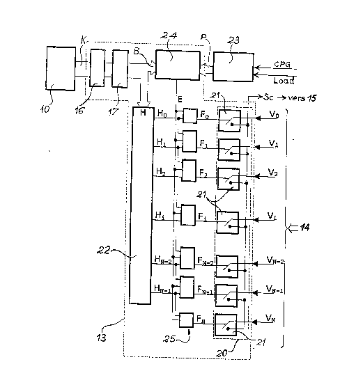
The invention also relates to an electronic control device
for the display columns. As shown in fig. 4, said device
comprises~
- a digital data source 10 supplying words K encoding the
information to be displayed on k bits (in the case of an
analog source, it is necessary to carry out an analog-digital
conversion of the data),
- a display controller 11 receiving synchronization slgnals
from the data source and controlling the dlfferent signals
for driving the control circuits 13 of the columns of the
display 15,
B 11596.3 DB
21~83~7
- 13 -
- a generator 14 of N+1 discreet voltages,
- the control circuits 13 of the columns of the display 15,
the controller 11 also being used for driving the row control
circuits 12.
The display column control circuits 13 are conventionally
constituted by a shift register 16 having k inputs and k x M
outputs, each output being associated with a storage flip-
flop 17. In other words, each column control circuit has
part of the shift register and k flip-flops. Each word K
stored in this way in the k flip-flops of a column control
circuit must be able to validate the control of a voltage
chosep from among N + 1. Thus, the control circuit comprises
multiplexing means. The original part of the device relates
to these means. Pig. 5 illustrates the formation of the
multiplexing means according to the invention. These means
compri~e a N bit blnary decoding circuit 22 (1 among 2n), a
comparator 24, a combinatorial logic circuit 25 and N+1
analog switches 21, all of whose outputs are connected to the
column output Sc of the channel in question and the analog
inputs are connected to the generator 14. The validation
inputs of these switches are determined in the manner des-
cribed hereinafter.
The word K supplied by the source 10 is subdivided into two
words H and B such that on having N+1 voltages, the word H
is constituted by h high order bits K, with 2h = N + 1, the
word B being constituted by the (k-h) remaining low order
bits.
On considering e.g. the binary word K: 11001110 for N=8, we
have h-3 and the word H will be constituted by the three
first bits, i.e.: 110 and the word B by the five last bits,
i.e.: 01110. The word H is used for determining the pair of
voltages (Vi, Vi+l) appropriate for the grey level to be
~"' ' ~-
B 11596.3 DB
21283~7
- 14 -
displayed and supplies the N bits 1 from among 2n binary
decoding circuit 22 in order to produce the N signals Ho to
HN_1 translating the encoding of H. ~:~
Thus, e.g. the following truth table of a three bit (1 among
8) (23=8) blnary decoder is obtained.
'.
inputs outputs
h2 h1 ho Ho Hl H2 H3 H4 H5 H6 H7
0 0 0 1 0 0 0 0 0 0 0 , '-':
O 0 1 0 1 0 0 0 0 0 0
0 1 0 0 0 1 0 0 0 0 0 :- ,
O `1 1 0 0 0 1 0 0 0 0 :,
0 0 0 0 0 0 1 0 0 0
1 0 1 0 0 0 0 0 1 0 0
0 0 0 0 0 0 0 1 0
0 0 0 0 0 0 0 1 , .
This example is given for a positlve logic-functioning
decoder (active output at state 1). It is also possible to
operate with a negative loglc-operating decoder, the impor-
tant thing is that there ls only a single valid output at
once, 80 as to only have one switch closed at a given time.
For this purpose the sequencer is provided and supplies the~ ;
index P of the addressing sequence within the row time, P ~-
being coded on (k-h) bits. This sequencer can e.g. be a
counter 23, whose clock CPG has 2(k h) pulses per row time,
said counter 23 being initiated for each row time (load
signal). The counter 23 can be an external counter or a
counter per circult. Thus E is a codlng bit, the comparator::
24 maklng lt posslble to carry out the comparlson of B and P
such that:
P ~B `E - 1
P> B~=~E = 0.
B 11596.3 DB -~
t ~ 7 ~ D
21~3~7
- 15 -
This coding bit E supplied the comparator 24 makes it poss-
ible to position in time the passage of Vi to Vi~l. The com-
binatorial logic circuit 25 between the signal E and the sig-
nals Ho to HN 1 makes it possible to obtain the signals P0
to FN, which drive the N+l analog switches and we obtain:
-
Fl = E-Ho + E-H1
Fi = E-Hi_l + -Hi
FN 1 = E HN-2 + E-HN_1
FN = E.HN 1
As sh~own in fig. 6, the generator 14 of N+l discreet voltages
can e.g. be constituted by N+1 operational amplifiers 30
connected as followers, with input voltages fixed by a resis-
tive dividing bridge Rl, R2, ... RN. In the pa,rticular caseof fig. 6, where the supply terminals of the divider bridge
are themselves voltag,e sources, the extreme voltages V0 and
VN are directly obtained twithout impedance matching by an
operational amplifier connected as a follower) from said
terminals. In the case of a linear distribution of the vol-
tages, the resistances Rl-RN will all have the same value,
otherwise their ratio will be calculated as a function of the
desired values V0 to VN.
However, this generator of N+l discreet voltages can also be
constructed, as shown in fig. 7, on the basis of one or more
digital-analog converters 31, which are driven by a control-
ler 32 responsible for calculating the values of the N+1
voltages and followed by amplifiers 33.
In cathode ray tube applications, it is generally possible to
choose to dlsplay a certain number of colours (or grey levels
for a black and white display) chosen from among a much
larger number, said functionality generally being fulfilled
B 11596.3 DB
~; 21283~7
- 16 -
by a specific so-called palette circuit. This operation i8
possible within the scope of the invention and the palette
circuit must then control the discreet voltage generator and
therefore the palette in accordance with the requirements of
the user.
Compared with EP-A-478 386, it should be noted that in
the implementation of the device according to the invention
the need to have equal time intervals leads to a simplifica-
tion, because the switching times are perfectly defined andare not dependent on any external parameter. Thus, it is
possible to use a simple CPG row subtime counter and operate
by comparison between the state of the counter and all the
bits constituting the low order of the data to be displayed.
In EP-A-478 386 the subtimes (signals TM) are externally
supplied, because the position of the tripping of the passage ~ --
from Vi to Vi~l is dependent on the characteristics of the ~-~
display to be controlled (the tlme constant Rs x Cs e.g.
varying with the display size).
B 11596.3 DB