Note: Descriptions are shown in the official language in which they were submitted.
SEI 94 16
TITLE OF THE INVENTION
' `
OPTICAL WAVEGUIDE MODULE ~ .
BACXGROUND OF THE INVENTION
Field of the Invention -~
:
The present invention relates to an optical
waveguide module which is used in an optical fibe~
communication network and others.
Related Background Art
' i 1
An optical waveguide module comprising, e.g., an
optical branching filter and others, generally comprises
a module unit which i3 formed by bonding end faces of
optical fiber cables with a respective end face of an ~:~
optical wavesuide and which is housed in a housing. In
the optical waveguide module, under the high temperature
and high humidity, an adhesive which is used in the
connecting portion between the optical waveguide and the
optical fibers moistens and is degraded, which causes the
degradation of characteristics: increase of loss and
light reflection, degrade of tensile strength.
Therefore, the housing is sealed with, e.g., a
nitrogen gas (Nz). Alternatively, the housing is filled
with a jelly-like resin. As such conventional
techniques, for example, a technique disclosed in
"Japanese Patent Laid-Open No. HEI 5-27139 (27139/1993)"
is known. A!3 a technique of coating the outside of the
housing with a resin, for example, a technique disclosed
'' ''
X ~t~ 3LJ~ ~3
SEI 94--16
in "Japanese Patent Laid-Open No. HEI 5-45531
(45531/1993)" is known.
SU~MARY OF THE INVENTION
~, It is an object o the present invention to provide
, S an optical waveguide module with high weather resistance .
and the long-term high reliability.
It is one object of the present invention to provide
an optical waveguide module comprising a module unit
, having a waveguide device with a waveguide substrate on
which an optical waveguide is formed, and a fiber
~ connector for holding a optical fiber cable, the .
¦ waveguide device being bonded to the fiber connector; a
j . housing for housing the module unit, the housing having a
;~ hole through which the optical fiber is inserted into ' `:
inside of the housing and is led out to outside of the :.
housing, and the housing a depth larger than a thic~ness
of th~ module unit; a member made of a resin covering a ::
bonding portion between said waveguide device and the
fiber connector, the member being filled in the housing,
the material being introduced in liquid-state into the
inside of the housing to immerse said bonding portion and
,, ,
thereafter being cured in the inside of the housing; and a :~
cover unit having a substantially flat shape for sealing :
said housing.
In this specification and claims, a waveguide-device
i, means a device including a wave~guide substrate itself, a
`'~ 2 ~ ~:
`~.'`' ~
~ :, '
~L2138~
SEI 94-16
device in which various optical elements are added into
the wave-guide substrate, or a device in which a
waveguide forming surface of the waveguide substrate is
covered with a resin etc.
According to the present ;nvention, since the
housing has a depth deep~r than a thickness of the module
unit, a connecting portion between the waveguide device
and the fiber connector can be immersed in a liquid resin
composition by filling the liquid resin composition into
the housing, and as the resin is cured, the connecting --
portion can be covered with the resin member. Therefore,
the module unit can be housed in a container cons~ituted
with the housing and the cover unit, and the module unit
¦ is contained in the resin member, so that the
characteristics are hardly degraded caused by the
moisture.
Further, a protective cover is provided at the
~, housing so as to project to the outside, which prevents
the stress to be applied to the optical fibers, and if the
protective cover is constitu~ed with an upper member and
, a lower member, works of assembling the module unit and
housing the module unit in the housing can be made
easier.
Furthermore, since the cover is made flat, the
waveguide module can be made very thin, and if a
'~ protrusion i.s formed on the inner rim of the housing, ~his
' 3 `-
' .
~21~ 8
SEI 94--16
protrusion serves as a sluice for the liquid resin
composition. The housing is bonded with the cover unit at
the outer rim by the adhesive.
The present invention will become more fully
understood from the detailed dsscription given
hereinbelow and the accompanying drawings which are given
by way of illustration only, and thus are not to be
considered as limiting the present invention.
Further scope of applicability of the present
invention will become apparent from the detailed
description given hereinafter. However, it should be `
understood that the detailed description and specific
examples, while indicating preferred embodiments of the
invention, are given by way of illustration only, since
various changes and modifications within the spirit and
scope of the invention will become apparent to those
¦ skilled in the art from this detailed description.
I BRIEF DESCRIPTION OF THE DRAWING
I
Flg. 1 is a perspective view showing a state of an
optical waveguide module before a module unit is
assembled in a manufacturing process of an optical
waveguide module according to the first embod~iment;
Fig. 2 is a perspective view showing a state of an
I optical waveguide madule after a module unit is assembled -i
} 25 in a manufacturing process of an optical waveguide module
according to the first embodiment; ~ -~
~ ` ~
;:
SEI 94-16
Fig. 3 is a perspective view showing a state of
liquid resin injection in a manufacturing process of an
optical waveguide module according to the first
embodiment;
Fig. 4 is a perspective view showing a state of an
optical waveguide module before a housing is sealed in a
manufacturing process of an optical waveguide module
according to the first embodiment;
Fig. 5 is a perspective view showing an appearance
of a completed optical waveguide module according to the
¦ first embodiment;
Fig. 6 is a perspective view showing a state of an
optical waveguide module before a module unit is
assembled in a manufacturing process of an optical
waveguide module according to the second embodiment;
Fig. 7 is a perspective view showing a state of an
~ optical waveguide module after a module unit is assembled
`I in a manufacturing process of an optical waveguide module
, ,~
'! ~ according to the second embodiment;Fig. 8 is a perspective view showing a state of
liquid resin injection in a manufacturing process of an - :`~
optical waveguide module according to the second -~-
embodiment; ;
Fig. 9 is a perspective view showing an appearance
of a completed optical waveguide module according to the
second embodiment;
",
: .~'.''
. . : ,.. ,1.
.
,,.~ '.
~21!~ 8
SEI 94-16
Fig. 10 is an exploded perspective view showing an
optical waveguide module according to the third
embodiment;
Fig. 11 is a vertical sectional view showing an
optical waveguide module according to the third
embodiment;
Fig. 12 is a graph sho~ing comparative experiment
results of the third embodiment;
Fig. 13 is a vertical sectional view showing an
optical waveguide module according to ~he fourth
embodiment;
Fig. 14 is a vertical sectional view showing an
optical waveguide module according to the fifth ~-~
embodiment; `~
Fig. 15 is a vertical sectional view showing an
~: .~ . .
optical waveguide module according to ~he sixth
embodiment; ;
Fig. 16 is a vertical sectional view of an optical
. :~
waveguide module showing a modified example of an
adhesive state of a waveguide substrate and a housing;
Fig. 17 is a hor zontal sectional view of an optical
waveguide module showing a modified example of an ~
adhesive state of a housing and a cover unit; ~-
Fig. 18 is a horizontal sectional view of an optical
waveguide module showing a modified example of an
adhesive state of a housing and a cover unit; and ~;
. i, .
.:~.',
~r~Z ~t~
'' .
, SEI 94-16
J Fig. 19 is a horizontal sectional view of an optical
waveguide module showing a modified example of an
adhesive state of a housing and a cover unit.
DETAILED DESCRIPTION OF THE PREFERRED EM~ODIMENTS
.. ,
The embodiments will be described below~ The same
components are represented by the same reference numerals
and the repetitive description on the same devices is
omitted.
Figs. 1-5 show a process of assembling an optical
waveguide module according to the first embodiment. Its -
structure will be apparent from the explanation of this
process. As shown in Fig. 1, a housing 10 has a long box ~ ;
,.
shape, and a large-diameter protective cover 11 having a
through hole to which a ribbon optical fiber cable 21 can ~~
be inserted is formed at the housing 10 so as to protrude
, from one end of the housing 10, and a small-diameter ~ .
protective cover 12 having a through hole to which a
~l single-optical fiber cable 22 can be inserted is formed -~
so as to protrude from the other end. The ribbon optical
~! 20 fiber cable 21 is formed by coating four bare fibers 23,-
234 made of silica glass individually with a resin layer
(not shown), arranging these fibers in a plane, and
integrating the fibers with internal and external resin
- layers (integral coating layer 24). The integral coating ,
layer 24 touches the inner surface of the hole of the
~ large-diam,eter protective cover 11. The single-optical
;
SEI 94--16
3 fiber cable 22 is formed by coating one bare fiber 230
with external and internal resin single-optical fiber
coating layers 25. The single-optical fiber coating
, layers 25 touches the inner surface of the hole of the
small-diameter protective cover 12. ~ `
The module unit 30 is fabricated by connecting fiber
connectors 31, 32 at both ends of a waveguide substrate
35. With the ribbon optical fiber cable 21 and the
single-optical fiber cable 22 are inserted into the -;
large-diameter protective cover 11 and the small-diame~er
protective cover 12, respectively, the module unit 30 is
assembl~d as shown in Figs. 1-2. First, the bare fibers
23~-234 and the bare fiber 230 are exposed from the ends of
the ribbon optical fiber cable 21 and the single-optical
lS fiber cable 22, and set in V-shaped grooves of a multi-
fiber V-shaped groove substrate 31A and a single-fiber V- ~-
shaped groove substrate 32A, respectively. Next, presser
plates 31B and 32B are put on the substrates and adhered
thereto to form a multi-fiber connector 31 which holds
~7 20 the bare fibers 23l-234 and a single-fiber connector 32
which holds the bare fiber 230. Note that the V-shaped
groove substrates 31A and 32A are fabricated by
mechanically grinding a silicon substrate or by
physically and chemically etching a silicon substrate.
3 25 Fig. 2 shows a state of an assembled module unit 3û,
and a waveguide substrate 35 lies between ~hese
.,li ' ' '
`', '' ' :
.~ .
,j
- ~2~34~3
SEI 94-16
connectors 31, 32. A lx4 branch type optical waveguide is
formed on a surface of the waveguide substrate 35. Such
an optical waveguide substrate 35 is fabricated by
depositing a plane lower cladding layer, a 1~4-branch-
lines-shaped core layer and a plane upper cladding layer,
and vitrifying these layers, using a method of depositing
SiOz fine particles on a surface of a silicon substrate
(FHD: flame hydrolysis deposition method). Next, both
end faces of the waveguide s~bstrate 35 are ~ixed with the ~ `
end faces of the multi-fiber connector 31 and the single- ~
fiber connector 32 by a photocuring adhesive (e.g., ultra ~`
violet ray curing adhesive). A protrusion 13 is provided
on the inner rim of the housing 10 so that the inner rim
is high and the outer rim is low. ~-
With a state shown in Fig. 2, as the ribbon optical
fiber cable 21 and the single-optical fiber cable 22 are
pulled toward both sides, the module unit 30 is housed in
the housing 10. Here, the depth of the housing 10 is --
sufficiently large as compared with the thickness of the
module unit 30 to entirely store the module unit 30 in the
housing 10. The housing 10 is fixed at the central part
of the base of the module unit 30 by the adhesive, and the
integral coating layer of the ribbon optical fiber cable
~ 21 and the single-fiber coating layer 25 are fixed to the
large-diamel:er protective cover 11 and the small-diameter
protective cover 12 by the adhesive, respectively. As
":'.;.
~']~
?~ L~f~
SRI 94 16
apparent from Fig. 2, the optical fiber cables 21 and 22
and the waveguide substrate 35 are arranged substantially
on one line. Accordingly, the optical fiber cables 21 and
22 are practically not bent. Therefore, this structure
is such that excessive stress is not applied to the
~, connecting portion between the optical fiber cables 21
and 22 and the waveguide substrate 35.
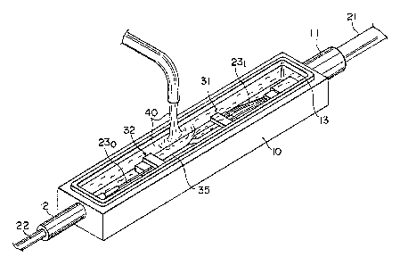
Next, as shown in Fig. 3, a liquid resin 40 ;~
i containing a jelly-like resin composition is injected and
filled into the housing 10. Here, since the housing 10
has a depth larger than the thickness of the module unit
30, the entire module unit 30 is immersed in the liquid
resin 40. Further, since the protrusion 13 is formed
along the inner rim of the housing 10, the liquid resin 40
~ 15 hardly overflows.
-j Next, the housing 10 is s~aled with a cover unit 15. ;~
A state before sealing is shown in Fig. 4, and a state
I after sealing is shown in Fig. 5. Here, the cover unit 15
has a groove (not shown) along the perimeter of the lower
surface corresponding to the protrusion 13 formed along
the inner rim of the housing 10. The adhesive is applied
' to the outer rim 14 of the housing 10, and the cover unit ~-
15 is adhered thereto. As described above, the optical
waveguide module according to the present embodiment is
completed.
~l In the above embodiment, the housing 10 and the
`i ' 1 0
~: .
~.2~ 8
SEI 94-16
cover unit 15 can be made of ceramic, plastic or metal,
e.g., Al (aluminum). various k:inds of adhesives such as -
an adhesive which cures upon light irradiation
(photocuring adhesive) such as a W ray, an adhesive
S which cures upon application of heat (thermosetting
adhesive), or an adhesive which cures upon mixture of two - i
liquids: a main agent and a curing agent, can be utilized
for an adhesive between the large-diameter protective
cover 11 and the integral coating layer 24, an adhesive
between the small-diameter protective cover 12 and the
single-fiber coating layer 25, an adhesive for the
formation of the multi-fiber connector 31 and the single-
fiber connector 31, and an adhesive between the housing ~ `
10 and the cover unit 15. For example, epoxy adhesive ~ ~
1 15 EPO-TEC 302-3 (manufactured by RIKEI CO., LTD) and epoxy ;i-
¦ adhesive STAYCAST 2057 (manufactured by GRACE JAPAN CO.,
I LTD) are used for an adhesive between the housing 10 and
! the cover unit 15, and ~he EPO-TEC is used for the
I formation of the multi-fiber connector 31 and the single-
¦ 20 fiber connector 32. Epoxy adhesive OPTDAIN UV-2100, 3100
I (manufacture by DAIKIN KOUGYOU COMPANY~ is used for the
connection of the waveguide substrate 35, the multi-fiber
connector 31 and the single-fiber connector 32. The
OPTDAIN contains a material having light (signal light)
transmission properties in which loss hardly occurs, and
is suitable f.or an adhesive between the optical waveguide
11 ' `
~2~8~'18
SEI 94-16
and the end face of the optical fiber.
On the other hand, as the liquid resin 40 for
filling, a resin which, before curing, is liquid with
high fluidity and which, aPter curing, is solid, e.g.,
gel, having a suitable elasticity is desirable. In
particular, the preferred properties are as follows.
First, it is superior in fluidity before curing and able
to fill a narrow space. Second, it is superior in
stickiness and adhesion, and has a sealing property and a
moisture resistance. Third, it is comparatively soft
after curing and easily transformed by small weight or
pressure. Fourth, it has a low elastic module after
curing and able to relax the stress due to thermal
e~pansion. Fifth, it has an oscillation absorptivity
i 15 after curing. SILICONE GEL (manufactured by SHINETU
SILICONE COMPANY) is an example of such a liquid resin 40. `~
XNR-4950 (manufactured by NIPPON CHIBA GAIGI COMPANY)
which is a super-reflective thermosetting epoxy resin, or
PERU-URETH~NE MU-102A~B (manufactured by NIPPON PERUNOX
CO., LTD) which is a two liquid mixture curing
polyurethane resin can be used.
Next, rePerring to Fig. 6-Fig. 9, an optical
waveguid~ module of the second embodiment will be
explained. In this embodiment, the module is also a lx4 ; ~-
branch type optical waveguide module, and the components
as same as Fig. 1-Fig. 5 are represented by the same
12 ~,
''~
' ~
SEI 94-16
reference numerals. As shown in Fig. 6 and Fig. ~, in ;~
this embodiment, the large-diameter protective cover 11
and the small-diameter protective cover 12 at both sides
of the housing 10 are constituted with lower half units 1
llA and 12A and upper half units llB and 12s,
respectively. The lower half units llA and 12A and the
housing 10 are integrally formed. These are easily
formed of a polycarbonate resin or a ceramic material. ~ ~`
This is because the large-diameter protective cover 11
and the small-diameter protective cover 12 are divided
into the upper and lower half units.
Further, since the large-diameter protective cover
11 and the small-diameter protective cover 12 are divided
into the upper and lower half units, a module unit 30 is -
easily assembled. ~hat is, in the first embodiment, as ~ ~;
shown in Fig. 1 and Pig. 2, after the ribbon optical fiber
cable 21 and the single-optical fiber cable 22 are
inserted into the through holes of the large-diameter
protective cover 11 and ~he small-diameter protective `
cover 12, the formation of the fiber connector 31 and the
single-fiber connector 32, and the connection of the
multi-fiber connector 31 and the single-fiber connector
32 to the waveguide substrate 35, that is, the assembling
- of the module unit 30 are performed. According to the
l 25 present embodiment, before the optical fiber cables 21
and 22 are installed in the housing 10, the module unit 30
13
., . ~.
. " .
SEI 94-16
can be formed. ~hen, after the module unit 30 is
completed, it is housed in the housing 10 without bending
~he optical fiber cables, so that the module unit 30 is ;~
not damaged by the excessive stress in the manufacturing
process.
As shown in Fig. 7, the module unit 30 is formed by
connecting a multi-fiber connector 31 for a ribbon
optical fiber cable 21 and a single-fiber connector 32
for a single-optical fiber cable 22 at both sides of a
waveguide substrate 35. Next, the module unit 30 is -
housed in the housing 10. The ribbon optical fiher cable -
21 is set and adhered in a groove of the lower half unit
llA of the large-diameter protective cover 11, and the
single-optical fiber cable 22 is set and adhered in a
groove of the lower half unit 12A of the small-diameter
protective cover 12. Next, the upper half units llB and
12B are bonded with the lower half units llA and 12A, so
that the housing 10 having the large-diameter protective
cover 11 and the small-diameter protective cover 12,
protruding from the both ends is formed. ~ -
As shown in Fig. ?, the upper half units llB and 12B ;
have substantially T shapes with holding parts for the `~`
optical fiber cables 21 and 22 as vertical axes, and their ;~
~ horizontal parts are put in cutouts at both ends of the
housing 10, whereby the housing 10 has a ho~ shape.
gly, as shown in Fig; 8, a liquid resin 40 is
2~
~1
..
SEI 94-16
~ injected into the housing 10, and the entire module unit
j 30 can be immersed in the liquid resin 40. Fig. 9 is a
perspective view of a completed optical waveguide module.
The same adhesive and liquid resin 40 as the first
embodiment can be used in this embodiment. According to
the second embodiment, after the module unit 30 is
~ assembled, it is set in the housing 10, so that the
;~ process is very simple and any excessive stress is not
applied to the optical fiber cables 21 and 22. Further,
the formation of the housing 10 is made easier. Ceramics
or plastic can be used as a material of the housing 10.
Further, the adhesive between the optical fiber cables 21
and 22 and the protective covers 11 and 12 of the housing
can be made perfect, so that the improvement of the
mechanical strength and the improvement of sealing
property can be achieved.
Fig. 10 is a perspective view of an optical
waveguide module according to the third embodiment, and
Fig. 11 is its vertical sectional view. In this -
embodiment, a ribbon optical fiber cable 21 and a single-
- optical fiber cable 22 are inserted into holes 152 at both `
ends of a housing 10 from the inside, and a module unit 30
is assembled and housed in the housing 10. Next, the
1 housing 10 is sealed with a cover plate 15 having a hole
151 at the central portion.
The above module unit 30 is formed by connecting the
. ~:
.
;~ 3L~f
. ..
t SEI 94-16 ~ ;
optical fi~er cables 21 and 22 at both ends of an optical . :
waveguide substrate 35. The optical waveguide substrate
35 is a silica waveguide substrate which is constructed
as a lx8 branch filter on an Si substrate by a flame
5 hydrolysis deposition method. Further, connectors 32 and
31 holding the single-optical i-iber cable 22 and the ;~
arrayed-multi-optical fiber cable 21 are fixed at both ;'
~ ends of the waveguide substrate 35 by an adhesive 301,
:l respectively. -~
f 10 The signal light incidence side of the optical ` :~
waveguide is coupled and aligned with the single-optical `~:
fiber cable 22 so that its optical axis matches an optical .:
a~is of an optical fiber 23 led out from the single~
optical fiber cable 22 through the left-hand side single- -
15 fiber connector 32. ~he signal light emerging side, :~
which is branched into plural (eight), of the optical : ;
waveguide is coupled and aligned with the waveguide .
substrate 35 so that their optical axes match optical ,~
axes of arrayed eight optical fibers 23 led out from the
~: Z0 ribbon optical fiber cable 21 through the right-hand side
multi-fiber connector 31. ~
. Each connector 31 and 32 has a V-shaped groove . :
formed on an Si chip, and the optical fibers 23 are
. inserted in the V-shaped grooves. End faces of the
25 . connectors 31 and 32 are fixed a~ the end faces of the waveguide substrate 35 using the adhesive 301. Further, .
' 16
.1 .,
3 ~.
-` 2~ 8
SEI 94-16
for the adhesive 301, an ultra violet ray curing adhesive
which is transparent against signal light and which has a
refractive index matching with refractive indices of the
optical waveguide and the optical fibers ~3 is used.
The holes 152 are formed at both end walls of the
housing 10. When the module unit 30 is provided in the
housing 10, the single-optical fiber cable 22 and the
ribbon optical fiber cable 21, which are connected to the
connectors 31 and 32, respectively are inserted into the
respective hole 152 and led out to the outside of the
housing 10. ~ote that a gap between the hole 152 and the
single-optical fiber cable 22 and a gap between the hole
152 and the ribbon optical fiber cable 21 are preferably `small, and these gaps are filled with the adhesive to fix ~-
the single-optical fiber cable 22 and the ribbon optical
fiber cable 21 at the housing 10.
As described above, the module unit 30 is provided
in the housing 10, and the single-optical fiber cable 22 !'~ `~';,
and the ribbon optical fiber cable 21 are led out to the
outside of the housing 10. Thereafter, a jelly-like
resin 40, e.g., a silicone gel as an elastic filling
material is poured into the housing 10 (see Fig. 11).
Next, an opening of the housing 10 is sealed with the
cover plate 15 having the hole 151.
In the above case, a larger amount of the jelly-like
resin 40 is]preferable and the resin 40 may fill up the ~ -
17
2~
.. .
~ SEI 94-16
; ;~ .
'~
~ housing 10 in order to pre~ent the moisture from
;, moistening the adhesive 301 of the connecting portion
between the optical waveguide and the bare optical fibers
23. However, in this case, the resin 40 may be expanded
according to hea~ depending upon the wor~ing temperature
and its volume becomes larger 1:han the volume of the inner
space of the housing 10. If the housing 10 has airtight
structure, the module unit 30 is expanded and the optical
connecting portion may be damaged. Thus, in the present
embodiment, the hole 151 is formed in the cover plate 15,
so that a part of the thermally expanded resin 40 flows
out through the hole 151, which solves the problem of the
e~p~nsion of the module unit 30. -
The inventors of the present application ~-
experimented a damp heat test t60C, 90% RH, 200 hours) in
a case of the module unit 30 provided in the housing 10
being covered with the jelly-like resin 40 and in a case `;
of not covered with the resin 40. The results are shown
in Fig. 12. In a graph shown in Fig. 12, a vertical axis
shows the amount of a reflection decrease, a horizontal ; `
axis shows the amount of a testing time in damp-heating - ~`
' and a white circle shows a the result in a module unit
' covered with jelly-like resin and a black circle shows
;~ .
the result in a module unit which is not covered with the
jelly like resin. It is recognized from the graph that a
reflective c:haracteristic of signal light is degraded at
18
--- z~
SEI 94-16
the connecting portion due to moisture moistening the
adhesive 301. ~;
In an optical waveguide module of the fourth
embodiment shown in Fig. 13, a cover plate 15 does not
have a hole, which is different from the third
embodiment, and a module unit 30 and a jelly-like resin 40
are housed in a housing 10, and the housing 10 is sealed
by the cover plate 15. The remaining structure is the
same as the third embodiment. In the fourth embodiment,
since the housing 10 is sealed, the optical waveguide ~ -
module may be used in water.
In an optical waveguide module of the fifth ` -;
embodiment shown in Fig. 14, the jelly-like resin 40 to be
contained in the housing 10 does not fill up the housing -~
15 10, which makes a space therein. An amount of the resin
40 is limited to the amount such that the amount of the
~xpanded resin 40 does not become larger than the volume
of the inner space of the housing 10 even though the resin ~ ~;
40 is expanded according to heat depending upon the
20 working temperature. Further, the cover plate 15 does
not have a hole, and the housing 14 is sealed with the
cover plate 15. Therefore, a coefficient of thermal
.~ .
expansion of the resin 40 is large, and in the case of the
~ resin 40 thermally expanded, the expanded resin 40 only
25 occupies the inner space of the housing 10, and the stress
due to the resin 40 is not applied to the module unit 30. `
19 ' ' .:
. ~ ~
~`' ''.` ,'
~2~
SEI 94-16
Accordingly, the connection loss betw~en the optical
waveguide and the end faces of the optical fibers does not
increase. `
In the sixth embodiment shown in Fig. 15, the
housing 10 is divided by two diiaphragms lO1 and 102, and
connecting portions between the optical waveguide
substrate i5 and the optical fibers 23 are located in two
regions formed between the diaphragm 101 and a side wall
and between the diaphragm 102 and a side wall. Further,
the jelly-like resin 40 .is contained only in these region ` ^
and provided for covering at least the connecting
portions. In this embodiment, only a minimum amount of
the jelly-like resin 40 required for covering at least
the connecting portions is contained in the housing 10, ~ ``
which makes the amount of the resin 40 very little. ~ ~;
Further, since the sufficient internal space i5 formed at -
the upper part in the housing 10 and especially the upper
surface of the waveguide substrate 35 is not covered with
the jelly-like resin 40, this embodiment is effective in
a case that an optical device such as an isolator or
others, an electrode for switching, or others are ~ ~
, ! integrated on the upper surface of the waveguide ~;
¦ substrate 35.
I ~ In the above-described embodiments, the silica
waveguide formed on a silicon substrate is used as the
optical waveguide substrate 35 but besides this, the
SEI 94-16
optical waveguide substrate can be made of semiconductor,
dielectric substance, glass or others. For the jelly-
like resin 40/ a silicone rubbler, a silicone grease or
~ others can be used besides a silicone gel, and especially
¦ 5 a resin which has high water resistance is desirable. The
module unit 30 may be fixed at the base of the housing 10
(Fig. 1-Fig. 9), may be floated in the liquid resin 40
(Fig. 10-Fig. 15), or may comprise a protrusion part 105
for supporting the module unit 30 at the base of the
housing 10 as shown in Fig. 16. The module unit 30 is
fixed with the upper surface of the protrusion part 105,
and the large-diameter protective cover 11 is fixed with
the ribbon optical fiber cable 21 by the adhesive 201, and
the small-diameter protective cover 12 is fixed with the
single-optical fiber cable by the adhesive 202.
The structure of a joint of the cover unit 15 with
3 the rim o the housing 10 may be constructed as the
3 horizontal sectional views of Fig. 17-Fig. 19. In Fig.
¦ 17, cutouts are formed on the cover unit 15 to fit with
the rim of the housing 10, and an adhesive 108 lies
~ therebetween. In Fig. 18, the protrusion is formed along
,`! ' the inner rim of the housing 10, and the protrusion is
'j formed along the perimeter of the cover unit 15
3~ ~ corresponding to the outer rim of the housing 10. The
adhesive 108 lies between the outer rim of the housing 10
3 and the protrusion of the cover unit 15. In Fig. 19, the `;
21 ~
~: `
SEI 94-16
.:
protrusion is formed along the inner rim of the housing
10, and the groove is formed a]ong the perimeter of the
cover unit 15 to fit with the protrusion on the rim of the
housing 10. The adhesive 108 lies between the outer rim
of the housing 10 and the perinleter of the cover unit 15.
Thus, as described above, according to the present -
invention, a housing the depth of which is larger than the
thickness of a module unit, so that the module unit is
easily immersed into a liquid resin composition.
Therefore, a connecting portion between an optical
waveguide and optical fiber cables is covered with an
elastic filling material such as, rubber, a jelly-like
resin or others, so that the prevention of the moisture
from moistening the adhesive of the connecting portion is
ensured. Further, the housing is sealed by a cover unit,
which improves the weather resistance. Therefore, an
optical waveguide module in which, under the high :;
temperature and high humidity, degradation of ~
characteristics, such as increase of loss and light ` - `
reflection, degrade of tensile strength or others does ~-
not occur and which has strength to the oscillation,
! simple structure, and high reliability can be achieved.
From the invention thus described, it will be
~ obvious that the invention may be varied in many ways. `~
Such variati.ons are not to be regarded as a departure from
the spirit and scope of the invention, and all such
22
t" '
SEI 94-16
modifications as would be obvious to one skilled in the `~
art are intended to be included within the scope of the
following claims.
3 The basic Japanese Applications No. 188348/1993
filed on July 29, 1993 and No. 154916/1994 filed on July
6, 199~ are hereby incorporateclby reference.
~ . . .
Y, ,,.
~,,.
3 :
23