Language selection

Search

Patent 2129336 Summary

Third-party information liability

Some of the information on this Web page has been provided by external sources. The Government of Canada is not responsible for the accuracy, reliability or currency of the information supplied by external sources. Users wishing to rely upon this information should consult directly with the source of the information. Content provided by external sources is not subject to official languages, privacy and accessibility requirements.

Claims and Abstract availability

Any discrepancies in the text and image of the Claims and Abstract are due to differing posting times. Text of the Claims and Abstract are posted:

  • At the time the application is open to public inspection;
  • At the time of issue of the patent (grant).
(12) Patent: (11) CA 2129336
(54) English Title: SELF-LOCKING HEAT SINKS FOR SURFACE MOUNT DEVICES
(54) French Title: DISSIPATEURS DE CHALEUR A VERROUILLAGE AUTOMATIQUE POUR COMPOSANTS MONTES EN SURFACE
Status: Expired and beyond the Period of Reversal
Bibliographic Data
(51) International Patent Classification (IPC):
  • H05K 1/02 (2006.01)
  • H01L 23/40 (2006.01)
(72) Inventors :
  • SOULE, CHRISTOPHER A. (United States of America)
  • KUZMIN, GARY F. (United States of America)
(73) Owners :
  • AAVID ENGINEERING, INC.
(71) Applicants :
  • AAVID ENGINEERING, INC. (United States of America)
(74) Agent: SMART & BIGGAR LP
(74) Associate agent:
(45) Issued: 1998-05-05
(86) PCT Filing Date: 1993-02-25
(87) Open to Public Inspection: 1993-09-02
Examination requested: 1995-01-05
Availability of licence: N/A
Dedicated to the Public: N/A
(25) Language of filing: English

Patent Cooperation Treaty (PCT): Yes
(86) PCT Filing Number: PCT/US1993/001678
(87) International Publication Number: WO 1993017536
(85) National Entry: 1994-08-02

(30) Application Priority Data:
Application No. Country/Territory Date
843,462 (United States of America) 1992-02-28

Abstracts

English Abstract


A structure for attaching a heat sink to an electronic package comprising a pin (10) having a compressible point (16), the
point being adapted to pass through aligned holes in a heat sink (40) and a printed circuit board (60) so that the point compresses
as it passes into two holes and flexes back to an expanded position after it exits the printed circuit board hole opposite the heat
sink thereby holding the heat sink to the board with the electronic package (50) therebetween.


French Abstract

Structure permettant de relier un puits de chaleur à un module électronique comportant une broche (10) à pointe compressible (16), la pointe étant adaptée pour passer dans les orifices alignés se trouvant sur le puits de chaleur (40), et une carte à circuit imprimé (60), de sorte que la pointe se comprime lorsqu'elle passe dans deux orifices et reprend sa forme allongée lorsqu'elle ressort de l'orifice pratiqué dans la carte à circuit imprimé se trouvant à l'opposé du puits de chaleur, maintenant ainsi celui-ci sur la carte, le module électronique (50) étant situé entre les deux.

Claims

Note: Claims are shown in the official language in which they were submitted.

- 7 -
1. A device for connecting a heat sink to an
electronic device on a printed circuit board comprising:
a shaft,
said shaft being cylindrical and having an
expanded top at one end, which top has a greater diameter
than said shaft,
a point,
said point being disposed on said shaft at
the end of said shaft opposite said expanded top,
said point having a larger cross-section than
said shaft, said point further comprising at least one
flexible member, flexure of which serves to reduce the
effective size of the cross-section for said point, and
biasing means comprising a cylindrical spring
surrounding said shaft and having a smaller diameter than
said point and said top, said biasing means being adapted
to engage said top and the heat sink when said device is
in use,
whereby when the heat sink is placed over the
electronic device on the printed circuit board, said
device is connected to the heat sink, so that said
biasing means is disposed between said heat sink and said
top and said flexible member flexes so that said point
may be inserted through a hole in the printed circuit
board, after which said flexible member unflexes, thereby
holding said device to the printed circuit board and at
the same time holding the heat sink of the electronic
device.
2. The device of claim 1 wherein said top is
cylindrical.

- 8 -
3. The device of claim 1 wherein said flexible
member comprises at least one prong, said prong having a
tapered surface.
4. The device of claim 3 wherein said point
includes a pair of prongs disposed adjacent to each other
but separated by a space, said prongs flexing towards
each other when said point is inserted into a hole in the
printed circuit board and unflexing after said point has
passed through the hole thereby securing said device in
place.

Description

Note: Descriptions are shown in the official language in which they were submitted.


W093/17~362 1 ~ 9 ~ ~ ~; PCT/US93/01678
~ELF-t-OC~T~G ~EAT 8INR8 FOR
8~RFACE MO~NT D~VICE~
Field of the Invention
5This invention relates to the field of heat sinks,
and in particular, the means for attaching heat sinks to
a circuit board or other similar device.
Backqround of the Invention
There is a strong trend on the part of the
lO electronics industry to increase the density of
electronic packaging on printed circuit boards and in
semiconductors in order to boost performance and reduce
cost. For example, with the increased density of the
circuity at the chip level, the number of input/output
(I/03 address lines is increased, and this improves
communication with other logic circuitry. One problem
ociated with increasing the number of pins on a
semiconductor package is the need to maintain or reduce
the assembly co t. As a result, surface mounts or small
20 outline packages have been developsd. Without a method
to remove the heat from these electronic packages,
however, their performance is restricted, as the packages
themselves do not contain means by which heat-can be
conducted away. Moreover, these packages do not
2~ incorporate the means by which a heat sink may be
at~ached, and the high density of electronic trace leads
emanating from the surface mount package severely
restricts the type of attachment method for any heat sink
which could be used. This is particularly important as
30 any attachment used to affix heat sinks to these surface
1..3~1~ packages requires that the leads of the package
remain accessible after the surface mount package has
~een attached to the printed circuit board. Also, any
proposed heat sink attachment must minimize the stress
35 load on and not damage the delicate leads of the surface

WO93/1753S PCT/US93/0167~8
mou~t~a~ age. If the leads are damaged by external
forces such as might occur in attaching or removing a
heat sink, the electrical connections between the surface
mount package and the circuit traces on the printed
5 circuit board may be broken.
In the prior art, heat sinks have been attached to
such packages by bonding the heat sink to the package
- with a thermally conductive epoxy that closely matches
the coefficient of thermal expansion of the plastic
l0 package. There are several disadvantages to this method.
First, the application of the epoxy adhesives are labor
intensive operations requiring proper mixing and the use
of special tooling to attach the heat sink to the
package. Further, these adhesives are somewhat
15 hazardous, creating a disposal problem. Once applied,
the heat sink cannot be easily removed from the package
in the event the package has to be replaced or repaired.
Summary of the Invention
The present invention relates to an improved heat
ZO sink attachment for electronic packages known as surface
mount devices or for those packages which employ surface
mount attachment technology either through direct
attachment of the surface mount device to the printed
circuit board or through the use of an electronic package
25 socket.
In the preferred embodiment, dissipating heat from
these surface mount electronic devices is accomplished by
a heat sink which contacts the top surface of the package
by means of a spring-loaded pin with a self-locking,
30 compressible point. The pin is generally cylindrical,
having an expanded top at one end and a pair of flexible
prongs forming the compressible point at the other. A
spring surrounds the shaft. In operation, the pin is
inserted through a hole in the heat sink, which hole is
35 too small to pass the expanded top. The point passes

W O 93/17536 212 9 3 3 ~ P(~r/US93/01678
through the heat sink hole, however. The heat sink is
placed over the package mounted on a board, and the pins
aligned with holes in the board. The points of pins are
preC-e~ through the holes in the board. This compresses
S the flexible prongs, and the point r~S~s through the
hole. When the point ultimately r~Cseq through the hole,
the flexible prongs of the pin re-~Yr~nA-s so that the
point then grasps the underside of the board thereby
holding the pin in place. The spring is disposed around
10 the shaft between the top and the heat sink, and it
provides a bias that forces the heat sink against the
package for good thermal contact. More than one pin is
usually used, and preferably, the application of force
from the spring- loaded pins should be symmetrical with
lS resFect to the surfase mount package. The pin or pins
may be easily removeG by compressing the prongs so that
~- the point will again slip through the hole in the printed
circuit board.
Brief Descri~tion of the Drawings
We turn now to a description of the preferred
emhoAiment, after first describing the drawings:
Figure 1 is a perspective view of a self-locking
pin of the present evention;
Figure 2 is a side view of the pin of Figure 1
25 attached to a heat sink; and
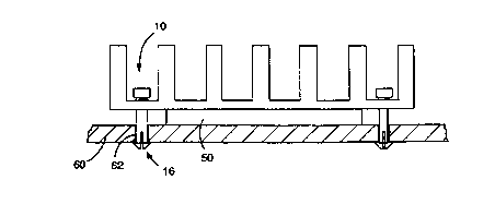
Figure 3 is a side view of the pin of Figure 1
showing the attachment of the pin to a heat sink, a
package and a printed circuit board.
Descri~tion of the Preferred Embodiments
Referring now to FIgure 1, a pin according to the
invention herein is shown at 10. The pin 10 is generally
cylindrical, and it comprises an enlarged, cylindrical
top 12, a shaft 14 and a point 16. A spring 18 is
di~oso~ around the shaft 14. The pin 10 is made of high
35 strength nylon in the preferred embodiment, although

W093/175~ PCT/US93/01678
2~?,93~6 , ~
- 4 -
other materials are possible. Preferrably, the overall
length of the pin 10 is .65 inches, with the shaft 14
being .46 inches in length, and .09 inches in diameter.
Other dimensions are, of course, possible, and in fact
5 I.Qc~c~-ry, A~renAi~q upon the size of the package, the
heat sink, and the thi~ness of the board and the size of
its hold.
As shown in Figure 1, the point 16 is comprised of
- a pair of prongs 20, 22 separated by a slot 24 which
10 extends into the shaft 14. The slot 24 is about .2
inches long from the top of the point 16 in the preferred
embodiment, and about .03 inches wide. Other dimensions
are possible. Each prong 20, 22 includes a tapered
surface 26, 28 which begins at an end 30 of the point 16
15 and eYr~nA~ back towards the shaft 14, together forming a
cone~ S~re bisected by the slot 24. As a result, the
prongs~20, 22 can be compre~se~ together slightly, but
when the compressive forces are released, they will
~eL~ll. to their original position, as shown in Figure 1.
20 The length of the surfaces 26, 28 is .10 inches in the
;~ ~ preferred emhoAiment and the maximum diameter of the pair
of prongs 20, 22 is about .140 inches. As with the other
- dimension of the preferred embodiment, different
dimensions may be used.
The operation of the pin 10 is shown in Figures 2
and 3. In Figure 2, a pair of pins 10 is shown attached
to a standard fin-type heat sink 40. Other types of heat
sinks may be used with this invention, however. In each
case, the point 16 of pin 10 is inserted through a hole
(not shown) in the heat sink 40 so that the point 16
projects below the heat sink while the top 12 and spring
18 are disposed on the opposite side; The diameter of
the hole ~not shown) in the heat sink is larger than that
of shaft 14 of the pin 10 so that the shaft 14 can move
35 up and down in the hole. The top 12 of the pin 10 is too
,~
,,~ ,
.,,, :
, ,

WO93/17536 PCT/US93/01678
---' 212933l~3
large to pass through the hole in the heat sink 40. In
general, at least two pins 10 are used for a given heat
sink, and usually four, positioned at the corners to
distribute the force as evenly as possible when the heat
5 sink is attached.
As shown in Figure 3, the pins 10 are used to
attach the heat sink 40 to a surface mount package 50 as
~ollows. The surface mount package 50 is mounted on a
printed circuit board 60. (Other electronic devices and
Io other supports may, of course, be used.) The board 60
has holes 62 which are disposed adjacent to the package
50. After the pins 10 (usually four) are placed in the
holes on the heat sink 40 as shown in Figure 2, the heat
sink 40 is then placed over the package 50, and the
15 points 16 of the pins 10 are then lined up with the holes
62 in the board 60 on which the package 50 is mounted.
Once aligned, the pins 10 are pushed down towards the
.
holes 62. As a result of the tapered surfaces 26, 28,
the point 16 slips into the holes 62. The sides of the
20 holes 62 compress the prongs 20, 22 together, and as
shown in Figure 3, the points 16 fits through the holes
62. Once through the holes 62, however, the prongs 20,
22 flex back to their original, uncompressed position,
and in so doing, grasp the underside of the board 60,
25 thereby holding the pin 10 in place without damaging the
surface mount package 50 or its electronic leads (not
shown). As shown in Figure 3, the heat sink 40 is then.
held in place against the surface mount package 50. The
springs 18: associated with the pins 10 serve to spring-
~
30 bias the heat sink 10 against the package to assure agood, thermally-conductive contact between the two~ The
pins 10 can easily be removed without damage to the
surface mount package 50 or its leads (not shown) by
compressing the prongs 20, 22 so that the pins 10 will

WO93/17536 PCT/US93/01678
?,~?.9336
- 6
slip through the holes 62. The spring 18 will assist
with this action.
It will be appreciated that one feature of the
invention is the variable pressure provided by the spring
5 loaded pins 10. This allows effective attachment while
reducing the possibility of damage to the package. It
will be further appreciated that shaft 14 can be
lengthened or shortened to accommodate different sizes of
electronic packages, and that the point 16 can be
10 enlarged or reduced to fit different printed circuit
board hole sizes or printed circuit board thicknesses.
It will be further appreciated that spring 18 could be
integrated into pin 10, and it will be further
appreciated that using existing molding capabilities,
15 either two or four pins can be manufactured as one
assembly.
While the invention has been described with
par~;r~llar reference to specific emho~iments only, it is
understood that the forms of the invention described in
20 detail are to be taken as preferred emhoAimentS thereof,
and that various changes and modifications may be
resorted to without departing from the spirit and scope
of the invention as defined by the claims.
What we claim is:
''~ :;
~ . .

Representative Drawing
A single figure which represents the drawing illustrating the invention.
Administrative Status

2024-08-01:As part of the Next Generation Patents (NGP) transition, the Canadian Patents Database (CPD) now contains a more detailed Event History, which replicates the Event Log of our new back-office solution.

Please note that "Inactive:" events refers to events no longer in use in our new back-office solution.

For a clearer understanding of the status of the application/patent presented on this page, the site Disclaimer , as well as the definitions for Patent , Event History , Maintenance Fee  and Payment History  should be consulted.

Event History

Description Date
Inactive: IPC from MCD 2006-03-11
Time Limit for Reversal Expired 2003-02-25
Letter Sent 2002-02-25
Grant by Issuance 1998-05-05
Inactive: Final fee received 1997-11-28
Pre-grant 1997-11-28
Notice of Allowance is Issued 1997-10-23
Letter Sent 1997-10-23
Notice of Allowance is Issued 1997-10-23
Inactive: Application prosecuted on TS as of Log entry date 1997-10-16
Inactive: Status info is complete as of Log entry date 1997-10-16
Inactive: IPC assigned 1997-08-14
Inactive: IPC removed 1997-08-14
Inactive: First IPC assigned 1997-08-14
Inactive: Approved for allowance (AFA) 1997-08-14
Inactive: Delete abandonment 1997-07-04
Inactive: Adhoc Request Documented 1997-07-04
Deemed Abandoned - Failure to Respond to Maintenance Fee Notice 1997-02-25
All Requirements for Examination Determined Compliant 1995-01-05
Request for Examination Requirements Determined Compliant 1995-01-05
Application Published (Open to Public Inspection) 1993-09-02

Abandonment History

Abandonment Date Reason Reinstatement Date
1997-02-25

Maintenance Fee

The last payment was received on 1998-02-04

Note : If the full payment has not been received on or before the date indicated, a further fee may be required which may be one of the following

  • the reinstatement fee;
  • the late payment fee; or
  • additional fee to reverse deemed expiry.

Please refer to the CIPO Patent Fees web page to see all current fee amounts.

Fee History

Fee Type Anniversary Year Due Date Paid Date
Final fee - small 1997-11-28
Excess pages (final fee) 1997-11-28
MF (application, 5th anniv.) - small 05 1998-02-25 1998-02-04
MF (patent, 6th anniv.) - small 1999-02-25 1998-10-16
Reversal of deemed expiry 2001-02-26 1998-10-16
MF (patent, 7th anniv.) - small 2000-02-25 2000-02-24
Reversal of deemed expiry 2001-02-26 2000-02-24
Reversal of deemed expiry 2001-02-26 2001-01-31
MF (patent, 8th anniv.) - small 2001-02-26 2001-01-31
Owners on Record

Note: Records showing the ownership history in alphabetical order.

Current Owners on Record
AAVID ENGINEERING, INC.
Past Owners on Record
CHRISTOPHER A. SOULE
GARY F. KUZMIN
Past Owners that do not appear in the "Owners on Record" listing will appear in other documentation within the application.
Documents

To view selected files, please enter reCAPTCHA code :


To view images, click a link in the Document Description column. To download the documents, select one or more checkboxes in the first column and then click the "Download Selected in PDF format (Zip Archive)" or the "Download Selected as Single PDF" button.

List of published and non-published patent-specific documents on the CPD .

If you have any difficulty accessing content, you can call the Client Service Centre at 1-866-997-1936 or send them an e-mail at CIPO Client Service Centre.


Document
Description 
Date
(yyyy-mm-dd) 
Number of pages   Size of Image (KB) 
Claims 1995-09-09 2 64
Abstract 1995-09-09 1 46
Cover Page 1995-09-09 1 20
Description 1995-09-09 6 329
Drawings 1995-09-09 1 21
Cover Page 1998-04-28 1 39
Representative drawing 1998-04-28 1 4
Commissioner's Notice - Application Found Allowable 1997-10-23 1 165
Maintenance Fee Notice 2002-03-25 1 179
Fees 2000-02-24 1 43
Correspondence 1997-11-28 1 27
Fees 1997-03-18 2 60
Fees 1996-01-30 1 79
Fees 1995-01-20 1 68
International preliminary examination report 1994-08-02 12 317
Prosecution correspondence 1995-01-05 2 60
PCT Correspondence 1994-08-16 2 50
Courtesy - Office Letter 1994-09-30 1 13
Courtesy - Office Letter 1995-05-02 1 31