Language selection

Search

Patent 2129778 Summary

Third-party information liability

Some of the information on this Web page has been provided by external sources. The Government of Canada is not responsible for the accuracy, reliability or currency of the information supplied by external sources. Users wishing to rely upon this information should consult directly with the source of the information. Content provided by external sources is not subject to official languages, privacy and accessibility requirements.

Claims and Abstract availability

Any discrepancies in the text and image of the Claims and Abstract are due to differing posting times. Text of the Claims and Abstract are posted:

  • At the time the application is open to public inspection;
  • At the time of issue of the patent (grant).
(12) Patent: (11) CA 2129778
(54) English Title: WAVELENGTH SELECTIVE OPTICAL SWITCH
(54) French Title: COMMUTATEUR OPTIQUE A SELECTION DE LA LONGUEUR D'ONDE
Status: Expired and beyond the Period of Reversal
Bibliographic Data
(51) International Patent Classification (IPC):
  • G02B 26/00 (2006.01)
  • G02F 1/09 (2006.01)
  • G02F 1/31 (2006.01)
  • H04J 14/02 (2006.01)
  • H04Q 3/52 (2006.01)
(72) Inventors :
  • CALVANI, RICCARDO (Italy)
  • VEZZONI, EMILIO (Italy)
(73) Owners :
  • AGILENT TECHNOLOGIES, INC.
(71) Applicants :
  • AGILENT TECHNOLOGIES, INC. (United States of America)
(74) Agent: SMART & BIGGAR LP
(74) Associate agent:
(45) Issued: 1997-09-02
(22) Filed Date: 1994-08-09
(41) Open to Public Inspection: 1995-02-11
Examination requested: 1994-08-09
Availability of licence: N/A
Dedicated to the Public: N/A
(25) Language of filing: English

Patent Cooperation Treaty (PCT): No

(30) Application Priority Data:
Application No. Country/Territory Date
TO 93 A 000 601 (Italy) 1993-08-10

Abstracts

English Abstract


The device includes a first and a second optical circulator having an input portand an output port that are the inputs and the outputs of the switch, as well
as an optical bandpass filter placed between the two circulators and
connected with means for switching its state so that the filter either reflects
or transmits a given wavelength, thus allowing a carrier with this wavelength
at the input port of one of the circulators to reach the output port of the samecirculator or the output port of the other circulator.


French Abstract

e dispositif comprend un premier et un deuxième circulateurs ayant une entrée et une sortie qui sont les entrées et les sorties du commutateur, ainsi qu'un filtre passe-bande optique placé entre les deux circulateurs et connecté avec des moyens de commuter son état pour que le filtre réfléchisse ou émette une longueur d'onde donnée, ce qui permet à une porteuse ayant cette longueur d'onde à l'entrée d'un des circulateurs d'atteindre la sortie du même circulateur ou la sortie de l'autre circulateur.

Claims

Note: Claims are shown in the official language in which they were submitted.

THE EMBODIMENTS OF THE INVENTION IN WHICH AN EXCLUSIVE
PROPERTY OR PRIVILEGE IS CLAIMED ARE DEFINED AS FOLLOWS:
1. Two-input, two-output optical switch, comprising:
a first three-port optical circulator with an input port and an output port
respectively forming a first input and a first output of the switch;
a second three-port optical circulator with an input port and an output
port respectively forming a second input and a second output of the
switch; and
a wavelength-tunable optical bandpass filter connected between an
input-output port of the first circulator and an input-output port of the
second circulator, and associated with means for switching it to either
of two possible states in which it respectively reflects or transmits a
given wavelength, so that a carrier with this wavelength arriving at the
input port of one of the circulators is transferred in a straight state to
the output port of the same circulator or in a crossed state to the output
port of the other circulator.
2. Switch according to claim 1, wherein the means for switching the state
of the filter is capable of making it reflect or transmit several
wavelengths that make up a wavelength-division multiplex present at
the inputs.
3. Switch according to claim 1, wherein said filter is a resonant cavity
optical fibre filter, associated with means to adjust the cavity length,
controlled by a variable voltage source for state switching and
wavelength tuning.

4. Switch according to claim 1, connected together with several identical
elements so as to form a n-input, n-output matrix.
5. Routing node for a wavelength-division multiplex optical
communications network, including a switching matrix implemented
with switches according to any one of claims 1 to 4.

Description

Note: Descriptions are shown in the official language in which they were submitted.


2~ ~977~
''.
The present invention relates to optical switching devices and more particularly it
concerns a two-by-two, wavelength selective opticai switch.
Wavelength selective optical swilches can be used for example in routing nodes of a
wavelength division multiplex network, i. e., a network in which information
associated to various communications or groups of communications modulates separate
20 carriers spaced apart by tens of nanometres to tenths of nanometre, depending on the
requirements and the technologies used. For such ~ppl ~i~ns, wavelength selectivity
is necessary, so that the various carriers can be routed along different paths.
Independence from polarisation is also desirable, so that polarisation state control
systems need not be introduced and attenuation wili not vary with the polarisation
25 state. On the other hand, the switching speed need not be very high, response times of
the order of some milliseconds being sufficient.
A polarisation independen~ switching element particularly suited for low switching
speed applications is described by A. C. Boucouvalas and G. Georgiou in the paper
"Fibre-optic interferometric tunable switch using the thermo optic effect",
30 Electronics Letters, Vol. 21, No. 11, May 23, 1985. The switch consists in an optical
fibre Mach- Zehnder interfetometre, in which the optical length of one of the two
branches can be varied through a heating eleclrode applied to a thin film connected to
the fibre in the branch. By applying adequate voltages to the electrode, the power
associated to an optical input signal is split as desired between the two outputs.
35 Thermo-optical switches based on the same principle can be used to form switching
matrices with several inputs and outputs, as described in the paper "Silica-based
optical- matrix switch with intersecting Mach-Zehnder waveguides for larger
fabrication tolerances" by M. Kawachi et alii, Conference OFC/IOOC '93, 21-26
. - ,. . . . . .

--~ 2~29778
February 1993, San José, California, (U.S.A.), paper Tu114.
The behaviour of thermo-optical switches, however, is substantially independent
from wavelength. Therefore, they must be coupled to optical bandpass filters forwavelength selective routing.
The lack of selectivity is also typical of waveguide switches using electro-optical
effects or semiconductor amplifiers as optical ports; moreover, such switches are
markedly polarisation dependent.
With this invention, on the contrary, a highly selective switch is provided that can
also be used in wavelength-division multiplex transmission systems having very
closely spaced channels.
The switch according to the invention includes:
- a first three-port optical circulator, with an input port and an output port
respectively being a first input and a first output of the switch;
- a second three-port optical circulator, with an input port and an output port
respectively being a second input and a second output of the switch; and
- a wavelength-tunable opticai bandpass filter, connected between an input-output
port of the first circulator and an input-output port of the second circulator, and
associated with means for switching it to either of two possible states in which it
respectively reflects or transmits a given wavelength, so that a carrier with this
wavelength arriving at the input port of one of the circulators is transferred to the
output port of the same circulator (straight state) or to the output port of the other
circulator (crossed state~.
Advantageously, the filter is a resonant cavity optical-fibre filter, associated with
means to adjust the cavity length for state switching and wavelength tuning.
The present invention will be made clearer with reference to the annexed drawing,
in which:
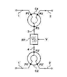
- Figure 1 is a diagram of the optical switch according to the invention; and
- Figure 2 is a diagram the electro-optical characteristic of the switch.
As it can be seen from Figure 1, the device has a pair of circulators, C1 and C2,
implemented in micro-optics, and a bandpass filter, FP, connected between the two
circulators.
Circulators C1, C2 are three-port devices having a one- way input port, a one-way
output port and a two-way input-output port. Input ports P1, P1' are the two inputs of
the switch, and are respectively connected to input lines 1, 1'; output ports P2, P2'
are the two outputs of the switchl and are respectively connected to output lines 2, 2'.
ports P3, P3' are respectively connected to fibres 3, 4 transferring signals from
circulators C1, C2 to filter FP and vice- versa.
The bandpass filter FP must have high wavelength selectivity and low attenuation
-. -. . .
~ : . . ,. :

-~ 2~2~778
and must be capable of transmitting th0 wavelength corresponding to the passband and
rejecting all others. For example, the filter FP can be a Fabry-Perot cavity resonatot,
in which a mirror at the termination of one of Ihe fibres 3, 4, and the other on the
surface of an element associated ~o the other fibre, said element having a size
5 comparable to Ihat of the cavity and practically the same refraction index as the fibre
core. A voltage-controllecl piezo-electric device allows shifting the element so as to
vary the cavity length and thus the filter passband. The structure of a tunable Fabry-
Perot filter is described for instance in the paper "A field-worthy, high performance
tunable fiber Fabry- Perot filter", submitted at the Conference ECOC '90, 16-20
10 September 1990, Amsterdam. The control voltage V of the piezo-electric device is
supplied by a source capable of generating several voltage levels, each of whichcorresponds to a passband centered around one of the wavelengths present on input
lines 1, 1'.
Both the optical circulators and the tunable Fabry- Perot cavity filter are
15 commercially available components.
The device works as follows. For simplicity, only one of the device inputs is
considered, say, input 1, on which a certain set of wavelengths, A1, A2...An, isavailable, and it is assumed that at a given time routing operations concern the carrier
at wavelength j. Depending on whether this carrier should be routed to output line 2' or
20 2, a control voltage V such that the resonator passband is centered on wavelength Aj
must be applied to the piezo-electric device of the filter FP.ln the first case, the
Fabry- Perot cavity of the filter is transparent to a radiation at that wavelength, and
carrier ~j passes from input 1 to output 2' through ports P1, P3 of circulator C1,
fibre 3, filter FP, fibre 4 and ports P3', P2' of C2 (crossed state of the switch). In the
25 second case, the radiation is reflected from FP along fibre 3 and leaves output 2
through ports P3, P2 of C1 (straight state of the switch).
Figure 2 shows the characteristic of a switch according to the invention for Aj=1548,45 nm. in the diagram, curve T depicts the percent power outgoing from portP2' versus the voltage applied to filter FP, and curve R depicts the corresponding
30 percent power outgoing from port P2. From these curves it appears that the crossed
state is obtained for V= 11,~5 V; if the voltage is increased to 11,65 V, the straight
state is obtained in turn.
At the moment considered, the switch also presents the same straight or crossed
state for a carrier at wavelength Aj that may be present at input ~': this carrier will
35 then leave through output 2 (along the path: ports P1', P3' of C2, fibre 4, FP, fibre 3,
ports P3, P2 of C1) if the voltage applied is ~he tuning voltage of the fil~er, whereas
otherwise it will be reflected by FP towards port P3' of C2 and will reach output 2'
through port P2'.
:
-~
.. ':

`- 2~2~778
.
The carrier to be routed can be selected by appropriately varying the voltage V.Generally, for a given voltage, the device will be in the crossed state exclusively for a
possible carrier which the filter is tuned to by that voltage, and will be in the straight
state for all others.
Several devices can be connected together to make up n-by-n matrices (n ~ 2), for
instance as shown in the paper by M. Kawachi et alii. Since a loss occurs in each
switch, as it appears from Figure 2, amplifiers must be introduced after a certain
number of seages in the matrix, for example, active fibre or semiconductor amplifiers,
to recover the signal level.
A device like the one described herein, besides being simple and easily implemented
with commercially available components, has indeed a high selectivity. Preliminary
evaluation of a filter having a spectral width of a few gigahertz, assuming that the
reflectivity of the two cavity mirrors is essentially the same, has shown that crosstalk
is negligible when adjacent channels in the wavelength division multiplex are spaced
apart by a few tenths of nanometre. Furthermore, the device behaviour is independent
from polarisation, since each of its components is polarisation independent.
It is clear that what described has been given only by way of non limiting example
and that variations and modifications are possible without going out of the scope of the
invention.
-, ~ .-. ~ ... , . ~- .. : . . . ... .

Representative Drawing
A single figure which represents the drawing illustrating the invention.
Administrative Status

2024-08-01:As part of the Next Generation Patents (NGP) transition, the Canadian Patents Database (CPD) now contains a more detailed Event History, which replicates the Event Log of our new back-office solution.

Please note that "Inactive:" events refers to events no longer in use in our new back-office solution.

For a clearer understanding of the status of the application/patent presented on this page, the site Disclaimer , as well as the definitions for Patent , Event History , Maintenance Fee  and Payment History  should be consulted.

Event History

Description Date
Inactive: IPC expired 2013-01-01
Letter Sent 2007-01-10
Inactive: Office letter 2006-10-31
Inactive: Office letter 2006-10-06
Time Limit for Reversal Expired 2006-08-09
Inactive: IPC from MCD 2006-03-11
Letter Sent 2005-08-09
Letter Sent 2001-06-07
Letter Sent 2000-08-15
Letter Sent 2000-05-12
Inactive: Multiple transfers 2000-04-11
Grant by Issuance 1997-09-02
Inactive: Status info is complete as of Log entry date 1997-06-27
Inactive: Application prosecuted on TS as of Log entry date 1997-06-27
Pre-grant 1997-04-14
Notice of Allowance is Issued 1997-03-04
Application Published (Open to Public Inspection) 1995-02-11
Request for Examination Requirements Determined Compliant 1994-08-09
All Requirements for Examination Determined Compliant 1994-08-09

Abandonment History

There is no abandonment history.

Maintenance Fee

The last payment was received on 1997-06-17

Note : If the full payment has not been received on or before the date indicated, a further fee may be required which may be one of the following

  • the reinstatement fee;
  • the late payment fee; or
  • additional fee to reverse deemed expiry.

Please refer to the CIPO Patent Fees web page to see all current fee amounts.

Fee History

Fee Type Anniversary Year Due Date Paid Date
Final fee - standard 1997-04-14
MF (application, 3rd anniv.) - standard 03 1997-08-11 1997-06-17
MF (patent, 4th anniv.) - standard 1998-08-10 1998-06-29
MF (patent, 5th anniv.) - standard 1999-08-09 1999-07-07
Registration of a document 2000-04-11
MF (patent, 6th anniv.) - standard 2000-08-09 2000-07-20
MF (patent, 7th anniv.) - standard 2001-08-09 2000-08-01
Registration of a document 2001-02-12
MF (patent, 8th anniv.) - standard 2002-08-09 2002-07-18
MF (patent, 9th anniv.) - standard 2003-08-11 2003-07-21
MF (patent, 10th anniv.) - standard 2004-08-09 2004-07-21
Owners on Record

Note: Records showing the ownership history in alphabetical order.

Current Owners on Record
AGILENT TECHNOLOGIES, INC.
Past Owners on Record
EMILIO VEZZONI
RICCARDO CALVANI
Past Owners that do not appear in the "Owners on Record" listing will appear in other documentation within the application.
Documents

To view selected files, please enter reCAPTCHA code :


To view images, click a link in the Document Description column. To download the documents, select one or more checkboxes in the first column and then click the "Download Selected in PDF format (Zip Archive)" or the "Download Selected as Single PDF" button.

List of published and non-published patent-specific documents on the CPD .

If you have any difficulty accessing content, you can call the Client Service Centre at 1-866-997-1936 or send them an e-mail at CIPO Client Service Centre.


Document
Description 
Date
(yyyy-mm-dd) 
Number of pages   Size of Image (KB) 
Abstract 1995-04-14 1 14
Cover Page 1995-04-14 1 34
Drawings 1995-04-14 1 30
Claims 1995-04-14 2 46
Description 1995-04-14 4 189
Cover Page 1997-09-01 1 37
Representative drawing 1997-09-01 1 4
Maintenance Fee Notice 2005-10-04 1 173
Fees 1998-06-29 1 38
Fees 1997-06-17 1 30
Fees 1999-07-07 1 27
Correspondence 2000-05-12 1 23
Correspondence 2000-08-15 2 51
Correspondence 2006-10-06 1 18
Correspondence 2006-10-31 1 16
Correspondence 2006-10-24 2 40
Correspondence 2007-01-10 1 14
Correspondence 2006-12-12 1 42
Fees 1996-07-04 1 29
PCT Correspondence 1997-04-14 1 32