Note: Descriptions are shown in the official language in which they were submitted.
21~99~~
IMPROVEMENTS IN OR RELATING TO
AIRCRAFT LANDING SYSTEMS
This invention relates to aircraft landing systems and more
especially it relates to scanning beam MLS (Microwave Landing
SS~stems).
As is well known to those skilled in the art, MLS systems
comprise two ground based beam scan lung equipments one of
which scans in elevation and the other of which scans in azimuth,
aircraft guidance information being derived by an airborne
receiver responsive to the scanned beams. One of the problems
associated with MLS is that the beams from which the airborne
receiver derives guidance can be affected by a combination of
MLS ground equipment errors and multipath effects dependent on
the local terrain.
This problem stems from the fact that MLS scanning beam
antennas produce a main beam and associated sidelobes. The
scanning beam sidelobes are distributed throughout the space in
front of the MLS ground based equipment and illumu~.ate any
multipath reflectors. The multipath reflectors in the case of the
azimuth ground equipment, can be buildings or elevated terrain
(hills) etc., and .may; or may not, be present at a particular
aerodrome runway location. The multipath reflector in the case of
the elevation equipment, is the ground and is therefore always
present at any location.
_ _7 _
The MLS regulatoz- authorities (ICAO, Eurocae, FAA, CAA)
specify a maximum limit on guidance error caused by the effect of
sidelobes reflected into the s~:111I11I1g beam by multipath
reflectors. They also specify that the MLS ground based
equipment shall shut itself down if the maximum specified
guidance ez-ror due to the effect of sidelobes and multipath is
exceeded. The MLS ground based equipment for elevation or for
azimuth comprises a phased array which is necessary to achieve
the high scan rate required. Each element of the phased array
must contain as a minimum, an electronic phase shifter. Failures
of individual array phase shifters cause the MLS array antenna
sidelobes to degrade and hence increase the effect of the sidelobes
on guidance via any multipath reflector.
It is therefore necessary to monitor in MLS ground based
equipment, the effects of sidelobes due to phase shifter module
failure via the multipath on guidance, and shutdown the MLS
ground equipmezzt when guidance due to this effect is out of
allowed tolerance. Furthermore, the moz~.toring mechanism
should shutdown the equipment only when erroneous guidance
due to sidelobes is possible, and not at any other time, ie. without
false alarms.
One known proposed method of monitoring the effect of
sidelobes, due to array phase shifter failures, which cause the
greatest increase in sidelobe level, is to have built in test (BIT)
within each phase shifter module and decide whether or not to
shutoff the equipment based on the degree and type of failure
and its position in the antenna array. This method requires BIT
2129~~~
within a large number of modules which is expensive and
additionally the decision making process requires software which
is not permitted within certain safet5- critical functions of MLS
because its integrity cannot be quantified.
An alternative known proposed method is to measure the
sidelobes of the scanning beam array directly, and to shutdown
the system when they reach a level which could cause false
guidance in the specified multipath conditions. The sidelobes
could be measured using a field monitor which serves to sample
the sidelobes transmitted by the ground based equipment or by
an integral waveguide monitor which produces a similar sidelobe
measurement. The sidelobe level at which the monitor goes into
alarm mode and shuts down the MLS ground equipment would
have to be that level which could possibly cause false guidance.
This method of monitoring the effect of sidelobes on
guidance, in its simple form as described above, is a problem in
that it will not satisfy continuity of ser<-~ice and mean time to
category downgrade requirements. This problem resides in the
effect of phase shifter module failures on the monitored sidelobes
~md their effect on guidance.
On the one hand, phase shifter failures in the centre of the
MILS array cause the largest increase in moautored sidelobes but
no increase in guidance error through the multipath. On the other
hand however, phase shifter failures approximately half way
along from the array centre ( depending on array amplitude
distribution) cause the maximum effect on guidance through the
multipath but cause the monitored sidelobes to increase by only
.~ _ 2~.2~94~
half the amount caused b~.~ pliase shifter failure at the array
centre. Therefore simply using the sidelobes as a method of
detecting false guidance due to effective sidelobes via the
multipath will cause the i~-IL~ ground based equipment to go into
alarm mode and shutdown unnecessarily if the phase shifter
module failures are at the centre of the array, ie. a false alarm.
It is therefore an object of the present invention to provide
an improved monitoring system which will shutdown the P.~LS
transmitter only when array failures result in an unacceptable
degradation of operational performance.
According to the present invention an MLS system
comprises ground based equipment which includes a microwave
signal transmitter arranged to feed microwave signals to radiator
elements of an array antenna via phase shifter modules one of
which is provided for each of the said elements, whereby the
production of a scanned microwave signal beam is facilitated,
signal monitor/detector means effective to provide a detected
sample signal derived from the scanned begun, filter means
responsive to the detectecj ;ample s:grlls for providing a filtered
signal derived in dependence upon effective sidelobe signals in
the said beam, and comparator means responsive to the filtered
signal for providing a transmitter shutdown signal when the ,
filtered signal exceeds a predetermined threshold level for more
than a predetermined time during a predetermined number of
successive scans.
Thus, as will hereinafter be more fully explained, although
the filtered signal is derived from sidelobes it is in effect weighted
-' - 21299~~
in accordance with their effect on guidance via multipath. In this
way false alarms are eliminated and the system is arranged to be
tolerant of phase shifter failures which might otherwise occasion
system downgrade to a lower reliability category, or even
unnecessary transmitter shutdown.
The signal monitor means may comprise a signal monitor, a
phase reference signal generator, and a phase sensitive detector,
the phase sensitive detector being responsive to a phase reference
signal provided by the said generator and to a sample signal
provided by th.e signal monitor for supplying the said detected
sample signal.
The filter means may comprise a differential amplifier
having two input ports and a delay device, which delay device
provides a delay corresponding to a period required for the said
begun to scan through a sector corresponding to one beam width,
the differential amplifier being fed at one port thereof with the
detected signal sample direct and being fed at the other port
thereof via the delay device with the detected sample signal.
alternatively the filter means may comprise a
capacitor/resistor differentiator circuit.
The comparator means may comprise a first comparator,
peak signal detector means responsive to the detected sample
signal for providing a threshold reference level signal which
defines the said threshold reference level, a counter, and a clock
pulse generator, the counter being triggered by the said first
comparator to count pulses from the said generator during periods
when a signal derived by the peak signal detector means exceeds
21299~~
the threshold reference le~~~~l Signal, the count being aggregated
during the said predetermined number of successive scans, and
the transmitter shutdown signal being produced consequent upon
the aggregated count exceeded a predetermined alarm level count.
The first comparator nay be coupled to the counter via gate
means operable in dependence upon the scanned beam position
for inhibiting signals derived from the main beam and passing
signals derived from the sidelobes.
The peak signal detector means may include a peak beam
detector which is responsive to the detected sample signal and
which is arranged to feed one port of a t~vo port sample and hold
eircuit and one port of a rivo port second comparator, the other
port of which second comparator is fed from the peak beam
detector via the sample and hold circuit to provide at the output
of the second comparator a feedback signal which is fed to the
other port of the sample and hold circuit so as to provide the
threshold reference level signal.
The comparator me6uis may comprise a third comparator
responsive to the count state of the counter for providing the
transmitter shutdown sign~~1 when the said count state exceeds
the said alarm level count.
The said ground based equipment may be used for the
purposes of providing a begun which scans in azimuth and similar
equipment may be provided which produces a beam which scans
in elevation.
1,
- % - 21299~~
One embodiment Of the lnV2I1t10I1 Will IlOW be described by
way of example only with reference to the accompanying
drawings, in which;
FIGURE 1 is a generally schematic block diagram of a part of
an MLS ground based equipment used to produce a scanned beam
Slgllal,
FIGURE 2 is a generally schematic block diagram of a part of
the equipment shown in Figure l,
FIGURE 3 is a generally schematic block diagram showing an
alternative circuit for a part of the equipment shown in Figure 2,
FIGURE 4 is a graph illustrating performance of the effective
sidelobe filters circuit shown in Figure 3 and Figure Z,
FIGURE S is a waveform diagram illustrating the waveform
to be expected at A in Figure 2,
FIGURE 6 is a waveform diagram showing the waveform to
be expected at BI in Figure 2,
FIGURE 7 is a waveform diagram showing the waveform to
be expected at BQshown in Figure 2,
FIGURE 8 is a waveform diagr~n showing a waveform to be
expected at C in Figure 2,
FIGURE 9 is a waveform diagram showing an alternative
waveform to be expected at point C lIl Figure 2,
FIGURE~10 is a graph showing a filter response illustrating
operation of a part of the equipment shown in Figure 2, and
FIGURE 11 is a generally schematic block diagram of an
alternative arrangement to the part of the equipment Shown In
Figure 2,
_'
212J9~~
Referring IlUW to Figur a ~ , 'AILS ground based equipment for
producing a scanning znicro~~:ave beam (used either for azimuth or
elevation) comprises a transnutter 1 which is arranged to feed an
RF power divider 2, which provides a plurality of output lines
only tyvo of which 3 and 4 are shown arranged to feed phase shift
modules 5 and 6 respectively. The phase shift modules are
arranged to feed a plurality of radiator elements such as the
elements 7 and 8 which are arranged to define a linear array
antenna 9. In operation of the antenna the radiator elements
which define the array- are energised to produce a beam the shape
and direction of which is determined in dependence upon the
setting of the phase shifter modules such as the modules 5 and 6.
In a practical implementation of the equipment the phase shift
modules are controlled to produce a beam which scans alternately
TO and FRO at a speed of ?0,000 degrees per second. In
equipment used to produce a scanned beam in elevation, the
beam width is an anged to be nominally 1.S degrees and the
corresponding beam width for azimuth scans is arranged to be
nominally 2 degrees. The construction of the equipment and
specification required is laid down by the regulatory authorities
as well known to those skilled in the art and accordingly will not
be discussed here in any great detail.
In order to provide a sample of the scanned signal, samples
from the array on a 1W a 10 are taken, or alternatively, a field
monitor apparatus 11 having a receiving antenna 12 is used
which provides a similar sample signal on a line 13. Although
both of the lines 10, 13; are shown in the drawing, (by way of
--.
2129944
example) it will be apparent that only one of the lines is used in
practice. The manner in which signal samples are produced is not
important and further discussion is therefore believed to be
unnecessary. Signal samples derived either via line 10 or line 13
are fed via a line 14 to an effective sidelobe monitor 15 which
utilises a signal on a line 16 from a phase reference generator 17
to provide an output signal on a line 18 when the effective
sidelobes monitored are unacceptable and this initiates shutdown
of the transmitter 1.
It should be emphasised that the monitor 15 does not
merely monitor the sidelobe level but measures the level of
effective sidelobes and shuts the transmitter down as appropriate
in dependence upon this measurement.
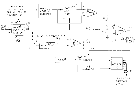
The construction of the effective sidelobe monitor 15 will
now be described with reference to Figure 2 wherein parts
corresponding to those shown in Figure 1 bear the same numerical
designations. Referring now to Figure 2, the effective sidelobe
monitor 15 comprises a phase sensitive detector 19 which is fed
with the phase reference generator signal on the line 16 and with
the sidelobe sample signal on the line 14. The waveform to be
expected at this point is as shown in Figure 5, which is a 5 GHz RF
signal envelope as might be seen on an oscilloscope at this point.
It will be appreciated that the actual 5 GHz RF signal would be a
blur and that the envelope only would be discernible. It will also
be appreciated that the waveform is shown as a function of time
as the beam is scanned from -60 degrees to +GO degrees with
uniform angular velocity of 20 degrees per millisecond and thus
- to - 2~,~994~
the horizontal axis which corresponds to the scan angle is also a
function of time. A field or integral monitor producing signals on
lines 10, 13 is arranged to monitor the array normal, ie. the scan
angle equals 0 degrees azimuth, hence the beam appears at this
angle in Figure 5. Thus at this angle a main beam 20 is shown
with sidelobes 21, 22, 23 and 24 which are due to the failure of
phase shift modules associated with a block of four radiator
elements 25 shown schematically in Figure 1.
The phase sensitive detector provides I and Qsignals on
lines 2G and 27 respectively and although as shown in Figure 2
the I signal is used in this example either of these signals could be
used for subsequent processing.
The signal to be expected on the line 2G designated BI is
shown in Figure 6. And the corresponding signal on the line 27
designated BQis shown in Figure 7. It will be appreciated that the
BI signal shovm in Figure G is produced when the antenna phase
cycling makes the beam phase the same as the phase of the phase
,,
reference signal on the line 1 G a.nd hence the beam is a maximum
at the BI output. The phase of sidelobes as shown in Figure 6,
which are due to the radiator element failures 25 as shown in
Figure 1, vary as the begun is scorning, the rate of change of
sidelobe phase being proportional to the distance of the failures
25 from the array centre and therefore the output signal from the
phase sensitive detector 19 on the line 2G as shown by the
waveform BI is an amplitude modulated frequency. The
amplitude modulation is the RF sidelobe envelope as shown in
Figure 5. The signal on the line 2G is fed to a sidelobe filter as
-11- 212994.
shown within broken line 28 which in this example comprises a
differential amplifier 29 and a delay line 30. The delay line is
arranged to provide a time delay which corresponds to the time
taken for the scanning beam to scan one beam width, which with
the beam widths and scanning rates specified is 75 microseconds
for elevation equipment and 100 microseconds for azimuth
equipment. The differential amplifier 29 is fed via the delay line
30 on a line 31 and directly on a line 32 from the phase sensitive
detector 19. The output signal at a point C on a line 33 from the
differential amplifier 29 is as illustrated in Figure 8 when the
antenna phase cycling causes the phase sensitive detector 19
output to correspond to the waveform shown in Figure 6. When
the waveform on the line 2C~ from the phase sensitive detector 19
corresponds to the waveform shown in Figure 7, a waveform
corresponding to the waveform shown in Figure 9 will obtain at
point C which is the line 33.
What should be appreciated is that if the four failures 25 as
shown in Figure 1 had been in the centre of the array, the
frequency of the sidelobe signal output from the phase sensitive
detector 19, Bl on the line 26, would have been zero but its
~unplitude would have been twice as large. Consequently four
Failures in the centre of the array would cause no output at the
effective sidelobe filter on the line 33 and this is precisely the
condition required because failures in the centre of the array thus
do not cause MLS guidance errors via multipath reflectors.
The signal on the line 3 3 is fed to one port of a two port
comparator 34 the other port of wluch is fed from a beam peak
_ 12 _ 21299~~
detector 35 via a sample ~ma hold circuit 36 a comparator 37 and
a potentiometer comprising resistors 38 and 39. An output signal
from the potentiometer 3 8 , 3 9 on a line 40 is thus fed to the
comparator 34 to sez-ve as an amplitude reference against which
the signal on the line 33 is compared.
The circuit for providing the reference on the line 40
includes the sample and hold circuit 36 because the peak beam
signal detected in a given scan will not, in general, be the largest
beam peak to occur during an antenna array phase cycle. The
peak sensed during each scan is therefore sampled and held by
the sample and hold circuit 36, the output of the sample and hold
circuit being compared with the latest beam peak and if the latest
beam peak is larger than the currently held value then the new
larger value is sampled and held.
Output signals from the comparator 34 are fed via a line 41
to a beam gate 42 and a signal is fed to the beam gate 42 on a line
43 so that the gate 42 serves to inhibit the main beam 20 which is
shown in Figure S and pass signals derived from the sidelobes 21,
22, 23 and 24. The signal on tl-ze line 43 is derived from
apparatus not shown which apparatus may also be used to control
operation of the phase shifter modules S, 6. Beam steering
systems for control of such phase shifter modules S, 6 are well
' ' ~ known and detailed description herein is believed to be
unnecessary.
Gated filtered signals on a line 44 from the beam gate 42 are
fed to initiate operation of a counter 4S which in the presence of a
signal on the line 44 starts to count pulses from a clock pulse
,.1
-13 - 22~994~
generator 4C~. The count registered by the counter 45 is compared
in a comparator 47 with an alarm level count as stored in an
alarm level count store 48 and when the alarm level count is
exceeded a transmitter shutdown signal is provided on the line
18. The counter is thus started when the signal on the line 33
exceeds the reference signal level on the line 30 as gated by the
beam gate 42 and if at the end of an antenna array phase cycle
the counter value exceeds about S% of the scanning beam time, as
indicated by the setting of the alarm level count in the store 48,
the transmitter shutdown signal is produced on the line 18.
In operation of the equipment it will be appreciated that the
phase sensitive detector 19 is required to detect the scanning
beam and sidelobe signals. The signal provided on the line l~
from the phase reference generator 17 must therefore be
coherent with the scanning beam and sidelobe signals but is not
required to be phase matched or phase stable over long periods of
time. The phase reference may conveniently be taken from a
source within the transmitter 1 or alternatively it may be
independently generated.
It will also be appreciated. that at the end of each array
phase cycle the counter 45 and the sample and hold circuit 36
should be reset.
Although an effective sidelobe filter as shown within the
broken line 28 and having a response as shown in Figure 10 is
preferably used, an alternative filter arrangement may comprise a
differentiating circuit comprising a resistor 49 and a capacitor SO
as shown in Figure 3, which is connected between the lines 26 and
- 1~ - 2~2994~
33. This circuit has a response as shown in the waveform diagram
of Figure 4 which although not as effective as the filter within the
broken Mlle ~ ~ shown in Figure 2, is nevertheless useful in
filtering effective sidelobes and for filtering lower frequency
components in particular, produced due to phase shifter module
failures.
Because the phase of the sidelobes incident on the phase
sensitive detector 19 input at the line 14 is varying continuously
as the beam is scanning, and at a rate which is related to the
effective sidelobes, the sidelobe signal is always present either as
an I signal on the line 2G or as a Qsignal on the line 27. However,
the scanning beam phase is constant during the scanning period,
and consequently it may be necessary to adjust the relative
phases of the scanning beam and phase reference to ensure that
the full scanning beam signal appears at the BI output on line 2G
moreover this phase adjustment would need to be fixed and
stable throughout the life of the equipment.
However, MLS ground based equipments frequently and
preferably employ antenna array phase cycling, ie. all the array
phase shifters are incremented prior to each scan or each TO/FRO
scan pair, consequently at some time during this phase cycle the
scanning beam input to the phase sensitive detector 19 and the
phase reference on the line 1G will have the correct phase
relationship so as to cause all the scanning beam signal to appear
at the I channel output and none at the Qcharmel output.
An alternative implementation of the effective sidelobe
filter, beam peak detector, sidelobe reference level and
- 1S -
~12'~9~~ .
comparator 28, 3S, 36, 37, 38, 39 and 34 is shown in Figure 11.
In this method, the I and Qoutputs from the PSD are digitised
using an analogue to digital converter S 1 and S 2.
The I channel is passed to a digital effective sidelobe filter
53. The I and Qchannels are passed to a digital pythagoras device
54 which forms the beam and sidelobe envelope. The output of
this device is passed to a digital peak detector S5 and then a hold
register 56. The output of the digital effective sidelobe filter S3 is
compared with the hold register S6 value in a digital comparator
57 the output of which is the same as 41 in Figure 2. The
remainder of the circuit is the same as Figure 2.
The theory of operation will now be considered. It is well
known, and can be demonstrated, that failures in the centre of the
array do not contribute to guidance error through the multipath
(effective sidelobes) but do raise the manifold dynamic sidelobes
more than any other failure. Consequently, detecting out of
tolerance effective sidelobe using the dynamic sidelobes is not
acceptable.
Considering firstly guidance error due to array module
failure, it can be shown that the beam pointing error due to array
module channel failure, amplitude failure (no output or stuck on
full output) or phase shifter failure (after integration over an
' ' antenna array phase cycle) is given by:
(Equation 1)
de=6. E(9R)IRI A1 sin k rdSme3
E A)~All ~ ~ r ( ~ ~ )I.sin(mR-k~i(1-cos(e+6R))[rdsinA~+Pz])
r
- m - 212J~J~:~
Where:
de - Beam pointing error due to array module channel
failure and multipath reflector.
83 - Antenna 3 dB beamwidth.
E(6R) = Antenna element pattern in the direction of the
multipath reflector.
E(e) - Antenna element pattern in the direction of the
receiver.
eR - The multipath reflector angle with respect to the
antenna array normal.
Pa - The range of the multipath reflector from the antenna
phase centre.
A - The receiver angle with respect to the antenna array
normal.
I R I - The amplitude of the multiparh reflection coefficient.
~R - The phase of tl~e multipath reflector coefficient.
An - The amplitude of the nth antenna array radiating
element.
EAn - The sum of all the antenna array radiating element
amplitudes.
A1r - The error amplitude of the rth element. In the case of
no output failure, Alr = Amplitude of unfailed element
(Ar). In the case of stuck on full output failure
A1r = Ar - 1. In the case of stuck phase shifter,
A1r = Ar,
r - The number of the failed element, N.B, the elements
are number 0 to N-1 where N is the total number of
i....\
-
array elements ( ~,'-~~ for 2 degrees azimuth or 1.5
degrees elevation i . .=~,rr ay element number n is:
n = 0, 1, 2, 3, ..........:~-1
r=n-[N-1]/2
Nf - The total number of failed elements.
k0 - The free space wave number (2~/~,0).
d - The antenna array element spacing.
It is not possible to kIlOW a priori the values of ~R and Pa.
Therefore, we must assume that they have values which make:
sin(QSR-k0( 1-cos(0+eP~) ) [rdsin6~+Pa]) - 1
for all values of r, ie. that the reflected signal phase always
causes the guidance error to be a ma.~imum.
Then the maximum possible beam pointing error is:
(Equation 2)
E( AR) IRI N'' sin03
d6m=83 E(e)~An ~ I.llrsin(l:Ord
r
d6m = Ma.~cimum value of de.
The equation for dem was derived assuming that the
~u~.tenna array phases pivot about the ~u-ray centre
The following conclusions can be drawn from this equation
(?).
(a) If Nr=1 (A single failure) then d6m is a maximum when
A~rsin(kOrdSiy~ ) I is a mwimum. This function has been
plotted for no output and stuck phase (see Figure 10). From this
plot, we see that the maximum value of d6m is at 4 or 4 positions
along the array for these r<vo Failure modes. The corresponding
-lg-
212~'~~~
curve for stuck or full output is I (Alr-1)sin(kprdsl2 3) I also
shown in Figure 10.
(b) If N~l, and is a contiguous block failure, r is continuous, and
the failures are at the 4 or 4 positions, then d9m is approximately
equal to the effective sidelobe allowance for the azimuth array
when Nr=4.
(c) Symmetrical failures about the centre of the array do not in
general cancel to give zero guidance error. Equation ( 1 ) shows
that they can cancel for particular values of r, ~R and Pa, but
since f~R and Pa are not known, it is not possible to identify those
failures which will be cancelled by a similar failure elsewhere in
the array.
Considering now integral waveguide monitor ( 10 in Figure
1) dynamic sidelobes, it can be shown that the dynamic sidelobe
voltage at the integral waveguide monitor output, due to array
modules failures, ie. does not include design sidelobes or tolerance
sidelobes, is given by:
(Equation 3)
Fl = -Alrexpj r1 Cd(kOsines+a) + ~'
NF-i
~ 1 + ~ expj(r-rl) Cd(kOsines+~3) + ~]
r=rl' r2 r3
When the variable names are defined above, and:
es - The array scan angle.
The integral waveguide propagation coefficient
( 2r~/~,g) .
~12994~
When the failures form, a contiguous block, ie. r=1. 2,
3..........Nr--1, then:
(Equation 4)
FI = -Alr expjrl [d(l;Osines;-(3) + r~
sin~F [d(kpsines+~3) + r,
l'~
Cd(kOsines+(3) + rl
sin
We see from the second expression that the failure sidelobes
of a contiguous block of array module failures form a failure
beam. (The function of the for-n sinNr-.v,% sinl.)
It can be shown that this failure beam has the following
properties:
(a) The peak of the failure beam appears at 10 in Figure 1 at
the same time as tile SCa11Il1I1g beam. (Beam due to perfect array
without failures.)
(b) The failure beamwidth is:
6F = 2sin-1 ~N d~ this is the null beamwidth.
(c) The peak voltage level of the failure beam (Vf) is:
NF A 1 r
where Ali, is the average failure amplitude
over the NF elements.
Example:
The worst case failure mode for guidance with no output or
stuck phase failure is four failures at the ~ or 4 positions. For the
.~~z array:
_20_
NF = 4, = 0.65, ~An = 39.7
Air
Then eF = 60 degrees
Vf = 0.0655 or -23.7 dB
For the same example, we can calculate d6m from the
equation (2) using the CAA specified reflection coefficient of -3
dB, E(eR) = E(6)
83 - 2 degrees (azimuth) then:
dem = 0.0728 degrees
This does not include the allowance for motion average (0.36
for high rate azimuth). When this is taken into account, the error
is 0.0262 degrees. The CAA specification is 0.03 degrees CMN.
(NB. The design and tolerance sidelobes will contribute a small
additional effective sidelobe error.)
Turning I10W to a method of sidelobe monitoring in
accordance with the present invention, the problem with sidelobe
monitoring can be summarised as follows:
Array module failures in the centre of the array cause an
increase in monitored dynamic sidelobes, but do not cause an
effective sidelobe increase.
The dynamic sidelobe voltage F1 given by equation ( 3 )
contains a multiplying phase factor,
expjrl ~d(kpsim8s + ~) + n]
From which we can see that the phase of the dynamic
sidelobe caused by a particular failure is changing with scan angle
6s. The rate of change of phase of the dynamic sidelobe phase is
proportional to the distance of the failed array module channel
~l -
from the array centre (assunung central phase pivoting).
Furthermore, symmetrical failures ha~~e equal and opposite phase
variation with scan.
Consequently, we can use this feature of the dynamic
sidelobes to distinguish those d5mamic sidelobes caused by failure
which are effective sidelobes from those which are not.
Considering now asymmetrical failures and in one specific
example, consider a block of four no-output or stud; phase
failures at either the 4 or ~'-i array positions. The failure beam
phase is:
r1 ~d(kOsines + (3) n~
The rate of change of failure beam phase with respect to
time is:
w dsa 0s Cr1(d~OsinOs + ~) + ;~~ ~ dd0 ~s ° aes
= rldk0 . cos0s . V
where: V = 20,000 degrees per second = 349 radians per
second
2~
r1 = 16, d = 30.5 mm (Azimuth), k0 = ~~ radians
per mm
2r
.. c~ = 16 x 30.5 x ~0 cosAs x 349
= 2838.5.2~c cos0s radi~ms per second.
The peals of the failure beam is at the same angle as the
waveguide manifold beam if As = ~10.~ degrees:
.. w - 2791 . 2~ radians per second.
- 22 - 2~.2~~~~
f = 2n - 2791 Hz
- 2.791 Hz
This is the frequency at the integral monitor beam position.
The lowest frequency for these failures will be when cosec is a
minimum, ie. when ~s is a maximum (40 degrees for HAz). Then
fD = 2.174 ICHz but at these wide scan angles, the manifold signal
will be in the failure sidelobes not the failure beam.
A similar block of four failures in the centre of the array
will havefD=0.
In order to detect the rate of change of phase of the failure
sidelobes, it is necessary to use a phase sensitive detector (PSD) to
detect the sidelobes.
Either the I or Q, channel outputs of the PSD may be used.
The output of, say, the Q.channel for the above case will be a
sinusoidal waveform whose amplitude follows the failure beam
and failure sidelobes and whose frequency slowly varies as the
beam is scanned. gut, most importantly, the output frequency of
the failure beam is related to the guidance error caused by the
failures in the desired manner, providing the high pass filter has
the correct transfer function.
For any single failure on one side of the array, the guidance
error function is 'plotted in Figure 10 for the extreme forms df
failure, ie. no output and full output (stuck phase has the same
effect as no output after integration of the sidelobe result over an
antenna phase cycle).
- ~~.~99~4
The dynamic sidelob~ level produced by no output failure is
proportional to the amplitude of the failed element Ar.
sin63
The guidance error is proportional to I Arsin(kord 2 )
(equation 2).
In this case, we need to multiply the dynamic sidelobe level
sin63
by sinCkord 2
The dynamic sidelobe level produced by full output failure
is proportional to ( 1-Ar), the guidance error is proportional to
sine3
(-Ar) sinCkord 2 ~. In this case we need to multiply the
S1I163
dynamic sidelobes level by S1I1 lord ~ as before.
In fact, dynamic sidelobes produced by any degree of
amplitude error of either sign should be multiplied by
sine3
sinCkord Z ' ~. 'this therefore should be the high pass filter
transfer function, shown plotted in Figure 10.