Note: Descriptions are shown in the official language in which they were submitted.
~162-38 2 ~ 3 ~
.. ,` 1
~. 1
ELEC$RICAL CONNE:CTOR
;'i':``'! " ,~ ,
~;~ 5
'-',
:-. .
'~
i'~ ,
FIE~D OF THE INVENTION .
The present invention relates generally to electrical
connectors and more particularly concerns electrical connector
assemblies with wadded wire contacts, recessed in apertures in -~
an interface module, for the transmission of electric current
~:l between male pins touching the wadded wire contact on opposite -
sides.
~ ~,
~ACRGROUND OF THB INVBNTION ~ ~ .
!; Electronic assemblies generally require multiple
electrical connections such that electrical signals and
current can flow from either a power source or a component
with electrical signals to other components of the assembly -~
via wires and cables. In those electronic assemblies, and
particularly those used in the air transportation industry,
durable and reliable connections must be made between the
electrical comporlents in order to properly transmit electrical
signals and current. Many different types of electrical
connectors have been used or proposed in the prior art. ;~
A common type of electrical connector is the pin and
socket connector. Unfortunately, the pin and socket connector
has been shown to have certain disadvantages. The pin and
k`~i sockst connector lacks the ability to provide efficient and
!'' reliable transmislsion of signals. Specifically, auxiliary
~,'
~, ~
'~,. :
~`!~.........
`~ 2~3~2~
contact area between the male and female contacts is critical
to insure that a reliable conn~ction is sustained in all
conditions. -~
For example, under conditions of vibration, as is typical
in the air transportation industry, the need for a large
contact area between the male and female contacts is
essential. If contact is lost along one point of the contact
area due to vibration, the auxiliary contact area assures the
existence of contact at other points of the contact area. In
addition, the possible presence of impurities in the contact
area accumulated either during the manufacturing process or -
from environmental exposure also compels the designer to
increase the contact area to prevent an interruption in the
flow of signals or current. The risk of improperly mating the
~5 assemblies generated by defects in the manufacturing process
or by the deformation of the parts after frequent engagement
Iil a~d disengagement further aggravates the problem. Thus, a -~
il substantial surface area of contact is essential to maintain
~1 an uninterrupted flow of electrical signals or current through
the connector.
Consequently, this enlarged contact surface area
~! decreases the degree of design flexibility for the connectors.
For inqtance, the number of connections that can be made
through one connector assembly is severely limited. The -
greater space required by one connection leaves less room for
;~ other connections. Furthermore, if a specific number of
'!",~. connection~ are required for one connector assembly, then the
size of the housing must be increased to accommodate the size
of the surface area of the male and female members.
When the size of individual connections is increased, the
weight of the connector assembly is increased correspondingly.
Further, more connector assemblies are needed to effectuate
the requisite number of connections due to the fewer number of
connections that can be made on each electrical connector
assembly. Thus, because each individual connection has
increased weight and further because more connector assemblies
are needed to complete the necessary connections for the
, ,.:
' ~''
'' ~ .
~, ~, 1 3 ~ 2 5 ~
-`~ 3
system, the total weight of the connector assemblies in a
~! system is increased. Naturally, weight is a significant
, concern in most industries and particularly in the air
`~ transportation industry.
l 5 A related disadvantage is tha~ a comparatively high force
is required to engage and disengage the connector assemblies.
The engagement force is a function of the surface area of
contact and the friction between the male and female contacts
which, in turn, is a function of the tightness of the fit
between those contacts. As previously noted, the surface area
of contact must be sufficiently large to avoid any potantial
break in the continuity of the electrical connection.
Furthermore, the frictional force between the contacts is
generally high as well to ensure a stable connection.
Hence, the person coupling the connector assemblies must
7, apply a significant force to engage the electrical contacts.
Likewise, disengagement demands a significant force. The
necessary insertion and disengagement forces are increased
3 with multiple contacts by each additional electrical
connection maintained through the connector assembly.
Furthermore, partially due to the necessary insertion
force, the male pins can become bent if inserted erroneously.
Subsequent insertion of the male pins into the female sockets
is consequently inhibited. Another disadvantage is that the
. 25 pins and sockets have relatively high electrical resistance.
:7,,
~j 8U~MARY OF TH~ INVENTION
It is the primary aim of the present invention to provide
an electrical connector of decreased size and reduced weight
, .~
while improving the integrity, durability and reliability of
the electrical connection. Accordingly, providing
environmental sealing from humidity and dust is a related
object. Another related object is to provide means for the
. .
electrical connector to withstand vibration, particularly of
the type common in aircraft.
Reducing the engagement and disengagement forces is
another important objective. A related object of the
:
. ~ . I
13~2~:~
invention is to provide guidance for the insertion of the
pins. An additional object is to facilitate the manufacture
-~ and assembly of the connector, particularly with regard to the
i insertion of the contact into the interface module.
'~ 5 Protecting the contact from wear and deformation is an
additional objective.
Another object of the invention is to provide flexibility
in the use of parts, but at the same time, prevent the mating
of non-compatible connectors with the improved connector. A
further object is to utilize existing wiring grommets, contact
rear release clip retention systems and pin contact retention
-`~ features currently defined and proven in U.S. government
specifications, including but not limited to MIL-C-83723,
MIL-C-38999 and MIL-C-39029. An additional object of the
invention is to utilize standard wire crimping tools and
~, insertion/removal tools, including but not limited to, the
,~r'`~ tools specified in U.S. government specification MIL-C-39029.
-, OthPr objects and advantages of the present invention and
its details of construction will be apparent from a
consideration of the following specification and accompanying ~-~
~, drawings.
In accordance with the present invention, an improved
electrical connector assembly is provided for linking an
~'~ electrical line to another electrical line. The
aforementioned ob~ects are attained through the utilization of
a resiliently compressible conduc~ive contact recessed in the
aperture of an interface module. The contact provides a means
across which electric signals and current can flow from one
.i male pin to another male pin without placing the pin~ into
direct contact.
The connector assembly includes at least one contact
retained within the aperture of an interface or contact
module. The interface or contact module is attached to a
retainment component with one or more openings therethrough at
positions corresponding to the opening in the interface
:.1
module. That retainment component is situated inside a shell
connectable to a second shell.
., ~
."j , ~:
,;i, .~ , ' ' ''
:
j` 213~2S:~
An advantageous feature of this electrical connector and
particularly the interface module is the reduction in diameter
of the opening in the interface module from one end to the
other end. The reduced diameter at the end of the opening
~ 5 which is exposed during use retains the contact within the
;~ interface module. In addition, assembly of the contact into
the int~rface module is facilitated by the enlarged diameter
in the opposite end of the opening in the interface module.
3 The contact is held in place after the interface module is
attached to the retainment component. Thus, the contact is
trapped in the interface module. In addition, the junction
between the retainment element and the interface module is
sealed from environmental exposure by a protrusion around each
~' opening in the retainment component that engages each opening -
in the interface module.
~`~ Further, to assure that the male pins contact the ends of-` the contact accurately, the connector assemblies use a
`i' "~ottoming" design. The connector assemblies are designed to
".'-J always connect with the shells of the assemblies directly
;~ 20 contacting axially to ensure the same relative axial position
';~ of each connection. In other words, the connector assemblies
are designed to invariably result with the assemblies in the
same relative axial position. Utilizing a datum reference at
the connection point between the connector assemblies further
advances the accuracy of the connection.
~!
BRIEF DE8CRIPTION OF TNE DRAWIN~8
;~ For a more complete understanding of this invention,
, reference should now be had to the embodiments illustrated in
greater detail in the accompanying drawings.
FIG. 1 is a perspective view of the connector of this
l invention;
3 FIG. 2 is a partial cross-sectional view along line 2-2
of the connector shown in FIG. l;
~` 35 FIG. 3 is an exploded, perspective view of the connector; ,
~ FIG. 4 is an enlarged partial view of FIG. 2;
!~` FIG. 5 is a cross-sectional view along line 5-5 of FIG. 2
:
. .~ .
!~,. .
6 2~ 3~2~ ~
.,
showing the interface module î and,
FIG. 6 is a cross-sectional view along line 6-6 of FIG. 2
showing the seal which mates with the interface module;
While the invention will be described in connection with
certain preferred embodiments, it is not intended to limit the
invention to those embodiments. On the contrary/ it is
intended to cover all alternatives/ modifications and
equivalents as may be included within the spirit and scope of
~j the invention.
,~ 1 0
DETAILED DE8CRIPTION OF THE: PRE:F13RRED EMBODIl~BNT~3 ; .f
~ Turning now to the drawings, FIG. 1 shows a perspective
,- view of the preferred embodiment of the connector 10 of the
present invention. The connector 10 comprises a receptacle 12
and a plug 14. As depicted in FIG. 1/ the receptacle 12 is
en~aged with the plug 14. The receptacle 12 and plug 14 are
designed to connect a group of wires 16, 18, 20, 22 which
extend from the ends of the receptacle 12 and plug 14. In
order to reduce the complexity of FIG. 1, only four of the
wires are shown. However, in this embodiment, two sets of
,~ thirteen wires could be connected by the connector 10. -
Referring to FIG. 3, the receptacle 12 includes a
coupling nut 28, receptacle shell 30, contact module 32,
contact 34, retainment component 36, pins 38 and coupling nut
attachment components 40. The plug 14 includes a plug shell
~1 5Q, a face seal 52l retainment component 54 and pins 56.
FIG. 2 provides a partial cross-sectional view through
one of the openings in the electrical connector 10. The wires
16, 20, are crimped or otherwise connected to the pins 38, 56.
The pin~ 38 and 56 are shown inserted through the
'J complementary openings in the receptacle 12 and pluy 14. The
pins 38, 56 protrude slightly into the contact module 32 and
`~ communicate with a resiliently compressible conductive contact
34 on opposite sides.
:! 35 The shells 30, 50 can be made of metal, preferably
~ aluminum, or a sturdy plastic material. The shells 30, 50
; have threaded portions 60, 62 so that the shells 30, 50 can be
, ..
'.'`, ,,:
.'RR;
2~3~2~:~
attached to other components. In addition, the plug shell 50
has a threaded portion 64 which engages the interior thr~ads
of coupling nut 28. The coupling nut 28 is rotatably attached
to the receptacle shell 30 by the coupling nut attachment
components 40 which are known in the art of electrical
connectors. Thus, the receptacle 12 is connected to the plug
14 by threading the coupling nut 28 onto the threaded portion
64 of the plug shell 50 until the coupling nut 28 is snug and
~ the shells 30, 50 are "bottomed out:". Of course, other
- 10 coupling means which are known in t:he art of electrical
., .
~, connectors can be used to connect the shells, including but
~' not limited to, bayonet coupling or lands and groove~
-l coupling.
The shells 30, 50 contain the retainment components 36.~, lS and 54. The retainment components 36 and 54 include openings
for the insertion of the pins 38 and 56 and wires 16, 20. The
retainment components 36 and 54 may be a singular integral
construction or preferably are composed of different
combinations of parts designed for adjacent affixation.
-~ 20 In this particular embodiment, the retainment components
36, 54 are composed of several different parts. Furthermore,
consistent with one of the advantageous features of this
invention, the retainment component 36 for the receptacle 12
is identical to the retainment component 54 for the plug 14.;¦ 25 Consequently, this feature greatly reduces the number of
individual parts required for the connector 10. As shown in
FIG. 3, the retainment component 36 is shown in the assembled
state and the retainment component 54 is shown in the exploded
state. Since both containment components 36, 54 are
identical, only retainment component 54 will be described in
~`l detail.
eferring to FIGS. 3 and 4, retainment component 54
~ includes a grommet 76, rear insert half 78, front insert half
.``!~ 80, insert retaining clip 82, and two positioning inserts 84.¦ 35 The retaining clip 82 is positioned in an opening 86 between
,¦ the rear insert 78 and the front insert 80. The rear insert
~ 78 and the front insert 80 are then attached to each other by,.1
~ 1
.
; l
- ~ ~ 3~2~
I
~i adhesive or other suitable means.
~l In order to properly align the apsrtures in the front and
-~ rear inserts 78, 80, two positioning inserts 84 are inserted
into grooves 86 on the front and rear inserts 78, 80. The two
positioning inserts 84 are then attached to the front and rear
~;~ inserts by adhesive or other suitable means. After the front
and rear inserts are attached to each other the retaining clip
82 is trapped between the front and rear inserts. At a later
stage in the assembly process, the clip 82 in used to hold the
~3 LO pin 56 in a relatively fixed position.
In order to complete the retainment component 54, the
grommet 76 is attached by adhesive or other means to t.he
~-~ opposite face of the rear insert 78. Thus, the front insert
;~ 80, rear insert 78, retaining clips 82 the positioning inserts
L5 84 and the grommet 76 are assembled to form the retainment
."~A component 54.
Each adjacent part should have the same number and
~l configuration of openings for the retainment of the pins 36
:i and 54. Separation of the parts provides flexibility in the
, 20 use of materials for the retainment components 36, 54. For
example, the grommet 76 can be composed of a soft material to ~1
provide sealing with the shell. Specifically, the grommet 76
!~ iS made of a resilient elastomer. However, the front and rear
!j inserts can be fabricated of a harder material in order to use
positioning flanges as will be discussed later. Specifically,
the front insert, rear insert and positioning inserts are made
~ of rigid plastic. Other combinations of materials may
''''3! additionally be employed without departing from the essence of
the invention.
I !30 Interposed between the receptacle 12 and plug 14 is the
-~ interface or contact module 32 which includes contacts 34.
The interface or contact module 32 is a cylindrical wafer 96
with at least one opening or aperture 98 therethrough. The
interface module 32 is made of a rigid plastic. The contact
~ 35 34~can be formed from a strand of a fine conductive metal wire
i wadded together to form a nearly cylindrical button. The
;~l wadded wire contact 34 may be of the type marketed by the
~, !
`l .
' ,' ~ ' ' '.:
2 ~ 3 ~3 2 Y~ ~L
~ 9
Cinch Connector Division of Labinal Components and Systems,
Inc., of Elk Grove Village, Ill., under the trademark
CIN::APSE. Similar suitable buttons are available from other
commercial sources.
~ 5 Referring now to FIGS. 2, 3 and 4 the interface or
,, ! contact module 32 includes at least one aperture 98 through
its thickness, but typically there are a plurality o~
apertures. Each aperture i5 defined by electrically insulated
material. The aperture 98 in the interface module 32 has
several different interior portio~s and extends from a first
~ face surface 100 of the interface module 32 to a second f'ace
I surface 102.
Referring to FIG. 4, the aperture 32 has a chamfered
portion 104 extending from the first face surface 100. As
will be discussed later, the chamfered portion 104 will be
~; used in conjunction with the seal 52 to create an
environmental seal for the connections. Moving to the left in
FIG. 4, the next portion of the aperture 98 is a tapered or
conical portion 106. Although the tapered portion 106 appears
to be cylindrical in FIG. 4, the diameter of the aperture is
greater at the left end o~ tapered portion 106 and gradually
~ reduces in diameter at the right end of tapered portion 106.
-~ The diameter at the left end is slightly larger that the
~¦ diameter of the contact 34. The diameter at the right end is
. . .
slightly smaller than the diameter of the contact 34.
This tapered portion 106 has several advantages. First,
the tapered portion 106 facilitates the insertion of the
contacts 34 into the aperture 98 because the diameter at the
left end i8 larger than the contacts 34. Second, the tapered
portion 106 prevents the contacts 34 from exiting the right
, end of the aperture 98 because the diameter at the right end
is smaller than the diameter of the contacts 34.
Consequently, as will be discussed later the tapered surface
106 allows the contacts 34 to ~e held in the apertures 98
without the risk of accidentally exiting the aperture 98.
A third advantage is that the contact 34 loosely fits
~¦ within aperture 98 and is free to slide within the aperture
...
~'1 .
;"~ .
:, 1 ;
-~ - 21~
'''; ` 1 0
98. ~his freedom of movement eliminates some of the problems
associated ~ith compressive engagement of the contacts in the
apertures. Impairment in the degree of resiliency i~ the
contact ~4 caused by compressive engagement is prevented.
Second, because the contact 34 may move when the pins 38 and
, 56 touch the contact 34, the centering of the contact 34
- within the aperture 98 is not critical. Furthermore, the
:~ loose fit between the contact 34 and the aperture 98 removes
;- potential variances in the compressive engagement of the
-` 10 multiple wire strand elements making up the contact end
~- sur~ace and removes the attendant unpredictability of the
electrical resistance.
Finally, moving further to the left in FIG. 4, the next
;, portion of aperture 98 is a recessed cylindrical or stepped
,~,i .
portion 108. The stepped portion 108 has a diameter which is
larger than the tapered portion 106. In assembly, the
! insertion of the contacts 34 in the interface module 32 is
'~j facilitated by the larger diameter stepped portion 108. While
,ij~j depicted in the drawing as stepped, this recessed portion 108
f~t 20 can alternatively be chamfered to guide the insertion of the
contact 34 into the aperture 98. In addition, as will be
discussed later, this stepped portion 108 facilitates the
assembly and alignment of the apertures of the interface
, module 32 to the retainment component 36.
After the contact 34 is inserted into aperture 98, the
interface module 32 is adhered or otherwise attached to the
l retainment component 36, or more specifically, the front
t/~ insert half 80. The retainment component 36 preferably has at
least one protrusion 114 which fits into the stepped portion
108. The inside diameter of this protrusion 114 is smaller
;l than the diameter of the contact 34. Thus, while the contact
34 can be easily inserted into the aperture 98 of the
interface module 32, the retainment component 36 prevents the
contact 34 from exiting the aperture 98 after assembly.
On the right side of the aperture 98, a reduced diameter
area prevents the contact 34 from moving beyond the point
where the diameter of aperture 98 is less than the diameter of
' .'.~.
~ . :
-- 2~3~2~
11
thfP contact 34. Accordingly, the contact 34 is trapped in
this aperture 98. Moreoverl this entrapment is effectuated
without any radial force exerted upon the contact 34.
As noted earlier, the aperture 98 includes a chamferPd
portion 104. This chamfered portion 104 forms a slope which
guides the pin 56 into the proper position for protrusion into
3 contact 34 when the receptacle 12 and plug 14 are engaged. A
malleable protrusion 118 on retainment component 54 engages
the walls of the chamfered portion 104 of the interface module
lo 32 to form a seal. This seal is in the nature of a "cork and
bottle" and protects the area of electrical contact from the
environment.
It is to be appreciated that the protrusion 118 may be
l~ integral with retainment component 54 or be attached as a
i~ 15 separate face seal 52. A separate face seal 52 offers added
interchangeability in the parts. The face seal 52 is made of
; a resilient elastomer. The dimensioning of the retainment
~ components 36, 54 of the connector assembly can intentionally
-~ be symmetric. Consequently, the retainment components 36, 54
can be used interchangeably with either the raceptacle 12 or
plug 14.
~ Another advantageous feature is that the male pins 38 and
- 56 protrude into the contact 34 on opposite sides without
overly compressing it. The pins 38 and 56 are designed with
flange areas 124 and 126 which engage abutment recesses 128 ~
and 130 in the retainment components 36, 54. In addition, the ;
~'~ flange areas 124, 126 on the pins engage the retaining clips
82. During assembly, the pins 38, 56 are attached to the
~;l individual wires 16, 20. Then the pins 38, 56 are inserted
into the apertures in the retainment components 36, 54 until i`
~;~l the flange areas 124, 126 of the pins engage the abutment
recesses 128, 130. As the pins 38, 56 are inserted into the `~
apertures, the retaining clips 82 engage the flange areas 124,
126 and prevent the pins 38, 56 from being removed from the
apertures. Conseg~uently, the pins 38 ! 56 are held in a
relatively fixed position.
Therefore, wh~en the receptacle 12 and plug 14 are engaged
'
'' . ' :'
``i}~: ~' 5~ f !~ t ` f - r ` ~ ~
-- 21392~
12
- with each other, th~ pins 38 and 56 can be inserted
sufficiently to contact and protrude slightly into the contact
34 as shown in Fig. 4, but the abutment recesses 128 and 130
will obstruct forward ~lovement beyond this point by engaging
the flanges 124 and 126. `
As can be seen, another advantageous feature of the
' invention is that the pin contacts and the retainment
i components are common to both the rleceptacle and the plug.
Consequently, this connector eliminates the need for socXet
~ 10 contacts and their associated rataiinment components.
;`l Furthermore, the connector uses standard wire crimping tools
and insertion/removal tools, including but not limited to, the
tools specified in U.S. government specification MIL C-39029.
FIGS. 3, 4, 5 and 6 illustrate another advantageous
feature of this invention that aids in the prevention of axial
compression on contact 34. The shells 30, 50 are designed to
"bottom out" when connected in order to consistently be in the
i same exact axial relationship when connected. When the
-~ receptacle 12 and plug 14 are engaged to be connected, the
plug 12 moves into the receptacle 14 until the shell 30 of the
plug 12 directly contacts with the shell 50 of the receptacle
14. In conjunction with the positioning features discussed
subsequently, this "bottoming" of the receptacle 12 and plug
14 ensures that the male pins 38 and 56 reliably touch the ;
contact 34 and do so without excessive compression.
The "bottoming out" can be performed by several means.
For example, predetermined threading on the shells 30, 50 in
~;~ conjunction with the use of keys 138 and notches 140 will
s assure that the connectors unite precisely. The keys 138 and
notches 140 assure that the starting point of the coupling is
always at the same location on the threading. FIGS. 5 and 6
illustrate the matching keys 138 and notches 140. In
addition, the accuracy of the alignment of the openings
between the receptacle 12 and the plug 14 will also be ensured
by the~e keys 138 and notches 140.
Axial alignment can alternatively be achieved by the
utilization of flanges situated on the shells 30, 50 at
.1. .~ .
' .
;,
~: - ;~
,
..;i
;;-J
- 213~
~;,
13
predetermined positions. When the flanges are clipped, pinned
or screwed together, the shells 30, 50 are consequently forced
; to meet in the same axial position. Thus, this invention
provides for the conduction of an electrical signal or current
, s fro~ a male pin 38 through the contact 34 to the male pin 56
without undue axial compression of the contact 34.
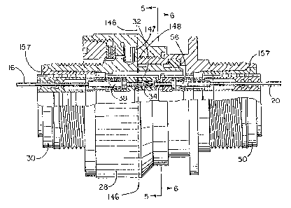
Furthermore, referring back to FIG. 2, in the
~` manufacturing and assembly process, drawings with datums
located at the point of attachment, plane 146, between the
edges 147, 148 of the shells 30, 50 are utilized. As all
measurements are taken from this datum point 146 where the
"bottoming out" occurs, a large tolerance build-up in the
, critical axially positioning feature is prevented. Indeed, no
tolerance build-up will exist at the point of contact and
"bottoming" of the connector halves is accordingly assured. -~
J Further, when the receptacle 12 and plug 14 are engaged
, as shown in Fig. 4, the annular shelves 150 and 152 on the
I interior of shells 30, 50 are an accurate distance from each
other. These shelves 150 and 152 axially position the
retainment components 36 and 54 by contacting the flanges 154,
156 on the retainment components 36, 54. The accurate
positioning of the retainment components 36, 54 will then
~ accurately position the flanges 124, 126 on the pins. The
:l ` flanges 124, 126 determine the axial position of the pins 38
and 56 with respect to the contact 34. The precise
positioning of these components assure that the pins 38 and 56 ~-
touch the contact 34 without undue compression.
While the annular shelves 150 and 152 obstruct the
retainment components 36 and 54 from forward movement, a
sealing material 157 is positioned between the interior of the
shells 30, 50 and the retainment components 35 and 54 which
functions as an adhesive and as a seal against the `
environment. The sealing material is a silicone-based
adhesive.
Additional advantageous features of this invention are
¦ the reduction in the frequency of bent pins and external
contact with the pins and contacts. Referring to Fig. 4, the
' .':
,~ 2~,3~2r31
. 14
pins 38 in the receptacle 12 are not exposed and the contacts
34 are housed internally in the interface or contact module
~ 32. Consequently, the pins 38 and contacts 34 are protected
` from external contact. Furthermore, in the plug 14, the pins
56 protrude slightly beyond the seal 52. Consequently, if the
user misaligns the receptacle 12 and plug 14, it is unlikaly
:i3 that the user will bend the pins 56.
^i It will be appreciated, of cou.rse, that the foregoing
arrangement is also suitable for non-cylindrical connectors.
For example, the receptacle, the plug, the retainment
1 components and the interface module can be rectangular in
.3 cross-section.
~ ,,
.! . ~
, - .
.~ ' ' ' ', .
,. ..
,,~ ' . '
~ .
'' ,' -::
.~ .
: .
,
3 `
. !
.'1 1
., .
" '"".
~ , ', .
'.'
r . I ~
i~`j _ .