Note: Descriptions are shown in the official language in which they were submitted.
2~3~39
-- 1 --
COMPOgITION AND M13THOD FOR OFF-AXIS GROWTH SIT13S ON
NONPOI-AR 8UB8TRAT~
Fi~ld o~ the ~nvention
........ . _
~rhis in~ention relates to surface preparation of
~onpolar wafers to facilitate epitaxial growth of polar
semiconductors.
~ckaround of the Invention
Growing polar semiconductors, such as III-V and II-VI
compound semiconductors, on nonpolar substrates, such as
silicon (Si) or germanium (Ge), is desirable for the
implementation of a variety of integrated electronic and
optical applications. Such applications include, for
example, optical interconnects between integrated circuit
chips, optical computing and photonic switching.
It is, however, difficult to grow compound semiconductors
on nonpolar substrates. The principal reason for this
difficulty is that there are no preferential bonding sites
for initial growth on the nonpolar substrate for the
cations and anions of the compound semiconductor. As a
~0 result, some growth may begin in the cation plane, and
~ome in the anion plane. This is referred to as antiphase
disorder. Further, differences in the lattice structure
e~ certain ~emiconductors, such as gallium arsenide (GaAs)
and S1, for example, present an additional impediment to
~5 ~atisfactory growth. Antiphase disorder and lattice
mi~match may result in both structural and electrically
actlvo defects.
The difficulty with growing compound semiconductors, in
particular GaAs, on nonpolar substrates, has been
Addres~ed in the prior art. See Fischer et al., "Growth
and Properties of GaAs/AlGaAs on Nonpolar Substrates Using
Molecular Beam Epitaxy," J. Appl. Phys. 58(1) at 37~-81
~19~5); ~iegelsen et al., "Heteroepitaxial Growth of Polar
Semiconductor~ on Non-Polar Substrates,l~ Mat. Sci. Eng.
,:: - - , ' . '
,.. ~ ' ' ~ ,.
~'. ' ' ' ,
2~3~3~
. - 2 -
sl4(3) at 317-331 (1992); Harris et al., ~The Nucleation
and Growth of GaAs on Si," Mat. Res. Soc. Symp. Proc.,
Vol. 91 at 3-14 (1987); Tran et al., ~Growth and
~haracterization of InP on Silicon by MOCVD," ~. Crys.
Grwth. 121(3) at 365-72 (1992); Sporken et al., ~Molecular
Beam Epitaxy of CdTe on Large Area Si<100>,~ J. Vac. Sci.
Tech. ~ 9(3) at 1651-55 (1991). All articles referenced
in this specification are incorporated herein by
reference.
One approach for growing compound semiconductors on
nonpolar substrates is to angle or tilt the substrate off
the standard <100> orientation. Se~ Harris et al. The
de~ignation "~100>" i9 known as a Miller indice. It may
be used to describe the orientation of a planar surface.
The <100~ surface refers to a surface which lies along a
face of a cubic lattice structure, and this is the
standard orientation for substrates such as silicon.
However, there are problems associated with using "off-
axis" silicon substrates for integrated electronics. In
particular, it has been found that device performance of
metal oxide semiconductor (MOS) transistors formed in off-
axis wafers i8 affected by this surface orientation. See
~hun~ et al., "The Effects of Low-Angle Off-Axis Substrate
~rientAtion on Mosfet Performance and Reliability," IEEE
Tran~. Electr. Dev. 38(3) at 627-33 (1991).
Others have explored the use of superlattice buffer
layers to minimize lattice mismatch between the substrate
and the compound semiconductor. To achieve growth of GaA~
on gi, Sakal et al., Mater. Res. Soc. Symp. Proc., Vol. 67
at 15 (1986) used a series of layers, beginning with a GaP
layer that i8 lattice matched to Si, then deposited
successive GaP/GaAsP and GaAsP/GaAs superlattice layers.
~esting of devices, such as a laser, formed utilizing
~uperlattice buffered GaAs/Si suggests that significant
3~ de~ects are still present. See Harris et al.
:
7,13~
- 3 -
Accordingly, there is a need for a method to grow
polar semiconductors on a standard orientation <100>,
nonpolar sub.strate.
8ummarY of tho Invent-lon
The foregoing problems are solved by the present
invention which provides a method for obtaining off-axis
growth sites on standard orientation nonpolar substrates.
According to a first embodiment of the invention, a
standard <100> wafer
with existing electronic structure is etched, at discrete
locations, through the dielectric films down to the
substrate surface. A film of erodible material such as
photoreRist or photo-definable polyimide is then applied
to the wafer surface. The intended growth regions are then
exposed to radiation which has an energy variation at the
surface of the erodible material. This results in an
angular taper in the material in the intended growth
regions. The profile of the erodible material is
transferred to the underlying substrate by use of an
etcher, obtaining an off-axis growth site ready for
compound ~emiconductor epitaxy.
Further ~eatures of the invention, its nature and
advantage~ wi 11 be apparent from the drawings and the
~ollowin~ detailed description of the invention.
Br~-~ D-,arlDtlon of Dra~ln~s
FIG. 1 is an illustration of a MOS structure formed
on a ~tandard substrate with a ~rowth site opened through
the MOS dielectric film;
FIG. 2 is an illustration of the wafer of FIG. 1
after application of a film of erodible material;
FIG. 3 is an illustration of the wafer of FIG. 1
after the film of erodible material has been selectively
expo~ed and developed;
, ' " ',
2~ 3~9 : :~
. - 4 -
FIG. 4 is an illustration of a photomask with
linearly graded regions ~or attenuation of optical energy;
and
FIG. 5 Ls an illustration of the wafer after etching,
~howing an o~f-axis isite ready for compound semiconductor
growth.
Detalled De~criDtion
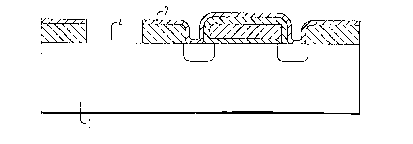
FIG. 1 is an illustration of a standard <100>
nonpolar wafer 1 with existing MOS structure 2 (without
metallization) which has been selectively etched through
the MOS dielectric films down to substrate surface 4. Any
means ~or etching through the films is acceptable.
Examples include, but are not limited to, reactive ion
etching, plasma ion etching, ion milling and wet chemical
etching.
After opening one or more growth sites 6, the sites
at which compound semiconductor growth is contemplated, a
film of selectively erodible material 8 is applied to the
wafer surface, as illustrated in FIG. 2. Suitable
erodible materials include, but are not limited to,
photoresists and photo-de~inable polyimide. The erodible
materlal 18 characterized by a change in solubility upon
e~o~ure to appropriate radiation, typically ultraviolet
li~ht, although x-rays or electron beams may be used with
2S certain materials. Exposure may increase or decrease
~olubility depending upon the nature of the erodible
materlal.
Th0 erodible material 8 covering the intended
compound semiconductor growth region or regions 6 is then
exposed to radiation. The radiation is applied so that
it has an energy variation at the surface of the portion
of the erodible material in the intended growth region 6.
~ft~r exposure, the erodible material i9 then treated with
a solvent that removes erodible material o~ higher
,' "' ,"",
},;-.; , , . , , . , . , .: ,: ,,,. . ,'.,, :',' . ' ' ' ' .. , ;
: " ~ " , , , , , , ............. , ~. ,.,, ., ,, , ,, , ,: ,,
, j ., , . .. , , .. . : .. : , .,, .: , :
2~ 37~ ~
solubility. This is referred to as ~development.~ After
development, an angular taper 10 in the intended growth
region 6 results as illustrated in FIG. 3.
To achieve the energy variation discussed above, the
halftorle, de-focused techniques described by D.R. Purdy,
"Fabrication of Complex Micro-Optic Components Using
Halftone Transmission Masks to Photosculpt Positive
Resist," EOS Top. Mtg. Dig. S., Vol. 2 (1993) and Hisanaga
et al., "Fabrication of 3-Dimensionally Shaped Si
Diaphragm Dynamic Focusing Mirror," Proc. IEEE Micro.
Electro. Mech. Sys. at 30-35 (1993) may suitably be used.
These techniques involve developing a photomask with a
predetermined variation in gray scale levels. When
photoresist is exposed through such a mask, the variation
in energy transmission will result in a complementary
variation in the depth to which the resist is exposed.
Focus is adjusted to introduce a degree of blur so that
the digitized nature of the photomask will not be
reproduced, resulting in a smooth surface at the
photoresist.
Another approach is to use a photomask 14 with
linearly graded regions 16, as shown in FIG. 4. The
~hotomask 14 illustrated in FIG. 4 would provide the
linearly varyin~ attenuation necessary to form four off-
~xl~ ~rowth regions, though such masks may be designed to~rovlde any number of such regions in any suitable
orientation. The linearly graded regions may be formed by
a thin film of chromium or iron oxide of appropriately
lncreasln~ or decreasing particle density. In a presently
~r0ferred embodiment, a thin film of inconel is used to
create a photomask according to a process developed by
Oxford Computer Inc., in Oxford, Connecticut. Film
thickness is varied to achieve a linear variation in the
energy incident upon the erodible material, resulting in
: ' . . .
. . .
.
.
:, . . , , ;
. . .
~ ~ 3 ~ ~ 3 ~
- 6 -
the tapered profile 10 as shown in FIG. 3 and discussed
above.
In a third method Eor obtaining the tapered profile,
which will be reEerred to as the scanned slit method, a
5 photomask comprising a slit of small width is positioned
over the portion of the substrate coated with erodible
material. The mask or substrate is held by a motorized
micropositioner. As radiation is directed at the erodible ;
material, the slit is scanned along the wafer, or vice
versa, for the distance desired to form the exposed area.
The rate at which the scanning occurs is varied to change
the amount of energy incident upon any particular section
of the desired area. The amount of erodible material
remaining after exposure and subse~uent development is
directly dependent upon the amount of energy to which it
was exposed. Thus, as energy is varied linearly along the
desired area, a taper or linear wedge 10 of erodible
material will result as illustrated in FIG. 3.
A fourth method for obtaining a tapered profile in
the erodible material is known as E-beam lithography.
This method involves the use of a scanning electron (E)
beam. In this method, a suitably programmed E-beam writer
i~ ~canned along the width of the intended growth region.
A number of ~anning passes are made across the width of
kh~ region, where, after each pass, the beam is indexed
alon~ the length of the intended growth region. Thus,
each ~can is performed at a slight lengthwise displacement
~rom the previous scan. In this manner, the full area of
~he intended ~rowth region i9 se~uentially expo~ed. A~
the E-beam i~ i~dexed along ~he length of the region, the
ener~y of the beam i8 varied as re~uired to alter the
exposure depth to provide the desired taper.
While the taper in the erodible material can be
achieved by the aforementioned lithographic methods, any
~ultable mean~ or method for achieving such taper may be
; . . ' . ' . ' ', : . ' ' :' '.
;.:~,., . . " . - .. . ... . . .... . . . ..
3 ~
. - 7 -
used and is within the contemplated scope of this
invention. It being recognized that other methods may
readil~ occur to those skilled in the art in view of the
teachings of the present invention.
Having obtained the taper 10 in the erodible layer,
as shown in FIG. 3, the wafer is then etched under
conditions which etch both the erodible material and the
substrate. In typical photolithographic applications, the
erodible layer remaining after development protects
underlying layers from the etchant, i.e., the erodible
layer is not etched. However, in the present invention,
the erodible layer is etched as well as the substrate.
This etching results in a tapered or angled off-axis
growth site 12 on the substrate wafer, as illustrated in
FIG. 5. The erodible material acts as a sacrificial mask
which provides a variable attenuation according to its
taper in order to transfer the desired shape or angle into
the underlying substrate. Reactive ion etching, plasma
ion etching, ion milling, wet chemical etching or any
other method or means suitable for etching both layers may
be used. While not practiced as often as the standard
~hotolithographic method, etching both layer~, as
~cribed above, is also well known to those skilled in
the art.
With regard to the desired taper angle of the growth
~ite 12, prior art 9tudies have determined preferred
an~ for compound semiconductor growth on nonpolar
~ub8trate0 such as silicon and germanium. For example,
~or GaAs epitaxial growth, a substrate taper of about 1/2'
3~ to 5' is recommended, and a 3' taper is most preferred.
See Masselink et al., "Optical Properties of GaAs on <100>
Si Using Molecular Beam Epitaxy," J. Appl. Phys. Lett.,
~5(12) at 1310 ~1984); Harris et al. and references cited
therein. As to other III-V compound semiconductors, Tran
et al. report that good quality InP on Si can be grown on
... . .
, ~ 1 ' ', ' I " ' " ,
,, , , .
:, . : .
. - 8 -
3- off-axis substrate. Sporken et al. found 6- to 8- off-
axi~ silicon pre~erable for the II-VI compound CdTe. In
all cases, the angle of the taper refers to the angle
~ubtended by the surface of the taper and the ~100>
surface, and the taper is towards the <110> surface.
The required angle of taper 10 of the erodible
material is determined by the relative etch rates of the
erodible material and the substrate, and the desired taper
of the growth region. Thus, if the etch rates of the
erodible material and the substrate are identical, the
de~ired taper in the erodible material would be 3 in
order to obtain a 3 off-axis substrate surface. If the
etch rates are not identical, the taper of the erodible
material would differ from 3- as a function of the
relative etch rates. In this manner, one or more off-axis
sites of the same or differing taper angle can be created
to provide growths sites for one or more of the same or
different compound semiconductors.
The present method has been discussed in the context
20 of wafers with existing MOS structure. However, it i9 ~ '
a~licable to wafers with any type structure (formed in
any ~itable manner), including, but not limited to
bi~olar transistor~, and heterojunction bipolar
tran~l~tors. Further, the aforementioned invention
de~cribes creating off-axis growth regions subsequent to
the creation of first level electronics and prior to
m~tallization. This i9 due to the fact that the current
~tate of the art for GaAs growth re~uires temperatures
above the melting point of MOS metallurgy. As GaAs growth
methods with lower growth temperatures are developed, or
as other metals with sufficiently high melting points are
u~ed for metallization, the growth regions can be created
~ubsequent to metallization of first level electronics.
To the extent that growth methods for other compound
semiconductors or other applications presently allow
., . , ~ , . . . . .. .
2 ~ ' 3 ~
g
growth after metallization, such embodiments are within
the contemplated scope of this invention. It is therefore
~nderstood that the present invention is not intended to
~e limited to preparing growth sites prior to
metallization. Further, growth regions can be created
prior to the creation of first level electronics. If this
is the case, then the initial etching step to remove the
dielectric films is not required.
After the off-axis growth sites are created in the
substrate wafer, compound semiconductors can be grown at
such sites by any method known to those skilled in the
art. Such methods include, but are not limited to,
molecular beam epitaxy, chemical beam epitaxy,
organometallic chemical vapor deposition (OMCVD), vapor
phase epitaxy and liquid phase epitaxy.
. ~., . : ~ . .:
,.,' ' , , , j, , .
... ~ , , ~ ; ' , ,:
:') ~ ' , ' ,' " ' '; " ' ' ' ,
,~ ' , ". ' . .,
. .