Note: Descriptions are shown in the official language in which they were submitted.
CA 02130825 2000-08-31
Method And Sensor For Measuring Electric Voltages
And/Or Electric Field Intensities
The present invention relates generally to a method for
measuring electric voltages and/or electric field
intensities, and to a sensor for carrying out this measuring
method.
Known methods and correspondingly used sensors of this
type are based on the principle of the linear electro-
optical effect of various crystals.
Measuring methods and sensors for such methods are
known, which are based on the principle that the refractive
index of certain crystals, which are transparent for light
waves, can be changed as a function of an electric field
intensity generated in the crystal. Crystals made of
lithium niobate or potassium dihydrophosphate, for example,
have this so-called electro-optical effect. Two electrodes
are arranged on a surface of a crystal wafer in parallel and
at a distance from one another, for example, for measuring
an applied voltage, by the resulting change of the
refractive index which is a function of the applied voltage.
For determining the refractive indices, interfero-
metric arrangements or polarimetric arrangements are known.
In the interferometric arrangement or method, the phase of a
light wave is modulated and superimposed on a reference wave
which leads to an intensity change of the coupled-out light
wave. In the case of the polarimetric arrangement or
method, the polarization of a polarized light wave is
changed as a function of the refractive index and the
intensity change is determined by a polarizer.
1
CA 02130825 2000-08-31
Both known arrangements require relative high technical
expenditures. In addition, the materials to be used cause
implementation problems. In addition to the requirement of
high electro-optical effects of the materials, there occurs
in these materials piezo-electric as well as elasto-optical
effects which together have the same appearance as the
purely electro-optical effect. The inertia of the material
will then have the result that, in the area of low
frequencies, the electro-optical effect on the one hand, and
the piezo-electric effect and elasto-optical effect on the
other hand, are superimposed on one another. The transition
range is also characterized by resonance phenomena which
result from crystal oscillations.
For a broad-band measuring system, the exclusive
utilization of the purely electro-optical effect is
required; that is, the corresponding piezo-electric/elasto-
optical effects must be negligible.
In the case of the polarimetric arrangement, this
situation must be met simultaneously for two coefficients,
while, in the case of an interferometric arrangement, one
coefficient will be sufficient. Therefore, a much larger
number of materials are available for the construction of a
broad-band interferometric measuring system than for a
broad-band polarimetric measuring system. However, a
disadvantage is the considerable technological expenditures
of an interferometer. In addition, integrated-optical
components must be used for this purpose, to which optical
power must be fed by a defined mode and by a defined
polarization. During the use of this technology in
2
CA 02130825 2000-08-31
practice, the use of a polarization-maintaining optical wave
guide (HiBi-fiber) is therefore absolutely necessary.
An object of the present invention is to provide a
method and a sensor for implementing the method by which the
advantages of the interferometric method can basically be
maintained, specifically the necessity of the evaluation of
only a single electro-optical coefficient. In addition, the
technical expenditures are minimized by the fact that
neither an integrated-optical technology is to be used, nor
must a special optical wave guide be applied.
According to this invention a method for measuring
electric voltages and electric field intensities uses the
electro-optical effect occurring in a crystal, in which the
field intensity in the crystal and thus the refractive index
of the crystal along a light path along a y-axis of the
crystal can be changed by a voltage applied across a z-axis
of the crystal transverse to the light path. The method
comprises: positioning one or more pairs of electrodes on
the crystal along the light path, the electrodes of each
pair being on opposed surfaces of the crystal spaced along
the z-axis; connecting an electric voltage to be measured to
the electrodes such that a gradient of the electric field
intensity in the z-axis occurs along an x-axis of the
crystal, and thus a gradient of the refractive index and, as
a result, a light wave in the crystal is deflected along the
x-axis as a function of the voltage to be measured;
transmitting a light wave along the light path; measuring
deflection of the light wave; and determining the electric
voltage connected to the electrodes from that measured
deflection.
3
CA 02130825 2000-08-31
The invention also provides a sensor for carrying out a
method of measuring electric voltages and electric field
intensities using such electro-optical effect occurring in a
crystal. The sensor comprises: a flat crystal having
opposed surfaces extending in the direction of its x-axis
and its y-axis and whose thickness extends in the direction
of its z-axis; two pairs of strip-shaped electrodes, with
members of each pair arranged on the opposed surfaces in a
mutually opposite manner, extending along the y-axis and the
pairs being spaced from each other long the x-axis; and
means connecting diametrically opposite electrodes of each
pair to each other and to an electric voltage to be
measured, such that a gradient of the electric field
intensity in the z-axis occurs along an x-axis of the
crystal and thus a gradient of the refractive index and, as
a result, a light wave in the crystal is deflected along the
x-axis as a function of the voltage to be measured.
The invention is particularly distinguished by the fact
that the light wave must only be sent through the crystal,
and must therefore be coupled in and coupled out. The
deflection of the light wave to be coupled out or of the
coupled-out light wave can be determined and evaluated by
simple devices.
Further advantageous details of the invention will
become apparent from the following detailed description of a
specific embodiment of the invention taken in conjunction
with the accompanying drawings, in which:
Figure 1 is a perspective view of a crystal to which voltage
is applied according to the invention;
Figure 2 is a top view of the crystal according to Figure 1;
4
CA 02130825 2000-08-31
Figure 3 is a view of the face of the crystal according to
Figure 1;
Figure 4 is a graph of the refractive index n in the
x-direction;
Figure 5 is a graph of the field intensity Ez in the
x-direction;
Figure 6 is a plan view of the possible course of a
deflected light wave; and
Figure 7 is a view of the arrangement of a sensor between
two spherical half shells provided in an electric field.
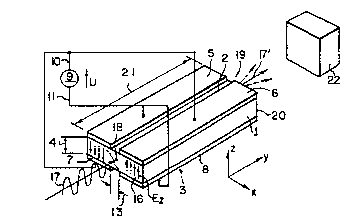
In Figure 1, reference number 1 indicates a crystal
made, for example, of lithium niobate. Its two surfaces,
top surface 2 and bottom surface 3, extend in the direction
of the x- and y-axes, and its thickness 4 extends in the
direction of the z-axis of the crystal l, as illustrated by
the coordinates. In the following, the coordinate data of
the x-, y- and z-direction will always refer to the crystal
axes. The two surfaces 2 and 3 are each provided with a
pair of strip-shaped electrodes 5,6 and 7,8 extending in the
y-direction. In this case, one pair of electrodes 5,6 is
opposite the other pair 7,8 of electrodes in a congruent
manner. Both pairs of electrodes 5,6 and 7,8 are connected
to a voltage source 9, so that the diagonally mutually
opposite electrodes 5,8 and 6,7, respectively, are jointly
connected with one of the poles 10 and 11 of the voltage
source 9. As a result, an electric field EZ in the z-
direction is formed between the electrodes 5 and 7, on the
one side, and the electrodes 6 and 8, on the other side;
however, these electric fields EZ are directed against one
another corresponding to the connection to the voltage
5
CA 02130825 2000-08-31
source 9. Because of the definition of the linear electro-
optical effect, therefore, for example, the refractive index
n of the crystal 1 is increased in one field and is reduced
in the other field (so-called Pockels Effect).
Correspondingly, a continuously changing field
intensity with defined field intensity gradients 14 as shown
in Figure 5, develops in the x-direction, in the area 12.
As a rule, area 12 is slightly larger than the distance 13
between the mutually parallel electrodes 5,6 and 7,8 in each
case in a surface 2 or 3. The refractive coefficient n in
the x-direction will therefore also change and a
corresponding gradient 15 is obtained, as illustrated in
Figure 4.
One of the faces 16, perpendicular to the y-direction,
is used for the coupling-in of a light wave 17 polarized in
the z-direction. In the embodiment, the coupling-in point
18 was selected in the center of the face 16. The coupling-
out point 19 may be provided correspondingly on the opposed
face 20. According to the desired measuring result, these
coupling-in and coupling-out points 18,19 may, however, also
be selected or provided at other points of the crystal 1.
By means of the above-mentioned arrangement, a voltage
or field measurement may be carried out as follows.
During the propagation of the light wave 17, which is
polarized in the z-direction, into the positive y-direction
of the crystal 1, the refractive index n appears with the
one electro-optical coefficient r33 (sole coefficient of
lithium niobate which is frequency-independent in good
approximation):
n = ne - 1/2 ne3rssEZ ( 1 )
6
CA 02130825 2000-08-31
wherein ne = 2,200 is the extraordinary refractive index,
and EZ is the outer electric field along the z-direction of
the crystal.
When the field intensity component EZ changes along the
coordinate x, the refractive index is also a function of the
location. The light propagation of the beamed in light wave
in the y-direction can then be described by the eikonal
equation:
grad ~(x)~ 2 = n(x)2 (2)
with ~(x) is the phase function of the optical wave. The
light wave will therefore follow the beam equation
d/ds(n(x) ~ dr/ds) - grad n(x) (3)
with s is the path length along the light path or the beam
propagation and r is the location vector. A possible
deflection of the light wave 17 is illustrated in Figure 6
by an interrupted and dash-dotted line.
From the solution of equation (3), the following is
approximately obtained for the location function of the
light beam
x = 1/a~(cosh(ay)-1) (4)
a = -1/2 noir33 dEz (x) /dx (5)
Small deflection angles gyp, while taking into account
the calculation at the emergence of the light wave 17' from
the crystal 1 with the beamed-through light path 21 and the
length L, can be estimated to be:
-1/2 n~fr~3 dEs (x) /dx L
7
CA 02130825 2000-08-31
As a result of equation (6), it becomes clear that for
the electro-optical deflection of the light wave 17, the
gradient of the field intensity EZ is relevant. Such a
field intensity graph can be implemented by the described
four-electrode arrangement.
By the appropriate coupling-in and coupling-out of the
light wave 17, for example, an intensity-modulated optical
signal can be obtained on an analysis unit 22 corresponding
to the time-related graph of the field intensity, which
signal corresponds to the voltage fed to the electrodes 5,6
and 7,8 or to a corresponding field intensity providing
voltage fed to the electrodes.
As illustrated in Figure 6, the coupling-in of the
light wave 17 may take place via a suitable optical wave
guide 23 which is coupled to the face 16, and the coupling-
out may take place via an optical wave guide 24 coupled to
the face 20. Preferably, the core or the core diameter 25
of the optical wave guide 24 provided on the coupling-out
side is smaller than the possible deflection range 26. As a
result, in the case of the shown centered arrangement of the
optical wave guide 24 with respect to the optical wave guide
23, the deflection can be recognized by an intensity change
of the light output beamed into the optical wave guide 24.
For the measuring of an electric field, according to
Figure 7, an arrangement consisting of two potential
surfaces 28 and 29 may be mounted in field 27, with the
crystal 1 therebetween. The potential surfaces 28 and 29
are made of a material which is electrically conductive at
least on one side, and which are constructed as spherical
half shells in the embodiment. Instead of being connected
8
CA 02130825 2000-08-31
to a voltage source 9, the electrodes are connected with the
potential surfaces 28,29. In the case of the existing
electric field 27, an electric voltage is induced on the
potential surfaces 28,29 which represents a measurement for
the field intensity existing there and can be measured. In
the case of this measuring arrangement and measuring method,
the sensor is therefore not connected to an external voltage
or voltage supply so that the otherwise resulting field
distortions can no longer occur.
The evaluation of the deflection of the coupled-out
light wave 17' or the light wave 17' to be coupled out
advantageously takes place via a photo diode or via a diode
line or via other photo elements, possibly a screen 30, as
illustrated in Figure 6.
The method according to the invention and the sensor
according to the invention which is used in this method may
be used for direct current or for low- and high-frequency
voltages, or for corresponding d.c. fields or alternating
fields.
As indicated in the description of Figure 1, the method
according to the invention and the sensor for carrying out
this method will also be completely operable if the crystal
axes x and y are rotated by 90° with respect to the
representation in Figure 1.
9