Note: Descriptions are shown in the official language in which they were submitted.
2~3~3~2
1 27879-31D
This is a division of application Serial No. 2,021,140
filed July 13, 1990.
FIELD OF THE INVENTION
The present invention generally relates to tunable laser
diodes and more particularly to a distributed feedback laser diode '~
having a diffraction grating as reflection means. :
~RIEF DESCRIPTICN OF THE DRAWINGS
- Figures lA and lB are diagrams showing an example of the
modulation of an optical beam used conventionally, wherein the ~ ~
optical output power from a laser diode is turned on and turned ' ~ :
off in response to a modulation signal to be transmitted;
Figures 2A and 2B are respectively a transverse cross~
sectional view and a longitudinal ~ross-sectional view of a prior :
art DFB laser diode;
Figure 2C is a graph showing a frequency versus
modulation characteristlc of the prior art DFB laser diode of
Figures 2A and 2B;
Figure 3 is a longitudinal cross-sectional view of
another prior art DFB laser diode and its modulation
- ~
characteristic;
Figure 4 1s a graph showing the operation of the DFB
laser diode of Figure 3;
Figures 5A and 5B are respectively a longitudinal cross-
seetlonal vlew and a transversal cross-sectional view showing a
first embodiment of the DFB laser diode of the present invention;
Figure 6 is a diagram for explaining the operational
principle of the DF8 laser diode shown in Flgures 5A and 5B;
Figure 7 is a graph showing the modulation
2~3~3~2
la 27879-31D ;.
characteristic of the laser diode of Figures 5A and 5B in
comparison with the conventional laser diodes;
: ,. ~
~ ~.
" :~..""_ ~., ,'.... "..''.' 'S,"''.' '
2~13~2
,
2 27879-31
Flgures 8A and 8B are graphs showlng the relatlon
between the osclllation wavelength and the optical output power of
the laser diode of Figures 5A and SB as a function of the drlve
current; :
Flgure 9 ls a block diagram schematically showing a
control system for maintainlng the optical output power constant
during the ~requency modulation of the optical beam; ~ ;
Figure 10 is a block diagram showing another control ~ -
system ~or maintaining the op~ical output power constant durlng
the frequency modulatlon of the optical beam; :i :;
Figure 11 is a graph showing the relationship between
the range of variable frequency and the size of the electrode
provided on the D~B laser diode;
Flgure 12A ls a plan view showing a part of the DFB
laser diode according to a second embodiment of the present
inventlon;
Figure 12B is a perspective view showlng a part of the
DFB laser diode of Figure 12A in a stat~ ~hat the laser diode is
sectioned transversally along a llne 12-12' of Flgure 12A;
Figures 13A - 13F are diagrams showing fabrlcation steps
of the laser diode of Figure 12A;
Figures 14A and 14B are diagrams respectlvely showing a
conventional mask used for providing isolation grooves in the DFB :
laser diode of Figure 12A and the isolation grooves thus formed
respectively; : -~
Figures 15A - 15C are diagrams showing the embodiments
of masks used in the second embodlment of the present invention
for forming the isolation grooves;
''. ''. , ',: . ' , : . . , ': . ' : ' : : ' , '
'" ' " :' ' ~ ~' , ' ' , ' ' : ~ ' , ' ' ' , j, ., . , . ' , '
~1313~2
3 27879-31
Figure 16 is a plan view showing a part of the laser
diode fabricated by the process of Figure 15D;
Figure 17 ls a schematical diagram showlng a process of
forming a diffraction gratlng with a ~4 phase shift reglon in the
corrugation forming the grating;
Figure 18 is a diagram showing the structure of a third
embodiment of the DFB laser diode according to the present
invention and the optical intensity distrlbution realized by the
structure;
Figure 19 is a diagram showing the structure of a fourth :~
embodiment of the DFB laser dlode according to the present
lnvention;
:::
Figures 20A and 20B are dlagrams showing the structure
of a flfth embodiment of the DFB laser diode accordlng to the :~
present invention and the dlstrlbution of the optlcal radiation
intensity obtained by the structure;
Figures 21A - 21E are dlagram~ showlng a process for :
forming the diffraction grating used in the DFB laser diode of
Figure 19 and Figure 20A; ~ :
Eigures 22A - 22F are diagrams showing a dlfferent
process for forming the diffraction grating used in the DFB laser
diode of Figure 20; and
Figures 23A and 23B are dlagram~ showing the structure
of a slxth embodiment of the DFB laser diode according to the
present invention together with the intenslty distrlbution of the .
...
optical radiation formed in the laser diode. ~ :
BACKGROUND OF THE INVENTION
In relation to the super-large capacity optical fiber
2:~3~ 36~ :
4 27879-31
telecommunlcation system of the next generatlon, the coherent
optical telecommunication system has been studled intensively. In
the coherent optical telecommunlcation system, the information is
modulated on a coherent optical beam by frequency shift keying
modulation or phase shift keying modulatlon and ls transmitted
along an optical flber network in the form of a modulated optical
beam.
The light, being an electromagnetlc wave, has frequency
components simllar to radlo waves. As the frequency of llght is
in the order of 200 THz, which is much higher than the frequency
of radio waves, an enormous amount of lnformation can be
transmitted when the light is used as the carrier of lnformatlon
transmission. ~ '
Flgures lA and 1~ show an example of the conventional
optical telecommunlcation process using the ordinary amplitude
modulation of the optical beam. In such an amplitude modulation
of the optical beam, a drive pulse havlng a magnitude exceeding
the threshold level of the laser o~cillation as shown ln Flgure lA
is applied to the laser diode, and the laser dlode produces an
optlcal output as shown in Figure lB ln response to the turning on
and turning off of the laser dlode. Alternatively, a separate
modulator for selectively passlng the optlcal beam produced by the
laser dlode may be usad. In this case, the laser dlode produces
an
~13~3~2
'' 5
1 optical beam with a constant optical output, and the
modulator absorbs the light in accordance with the
information signal to be transmitted. As a result, an
optical output similar to that shown in FIG.lB is
obtained.
In the optical telecommunication system based
on such an amplitude modulation of the optical beam,
however, the wave nature of the light is not fully
utilized. As the light has, as already described,
frequency components similar to the radio waves, it is
expected that a more efficient optical telecommunication
system can be achieved when the wave nature of the
optical beam is exploited, for example, in the form of
frequency modulation. -
Meanwhile, it is known that there are laser
diodes which can change the oscillation frequency in
response to the modulation of the drive current. In
other words, the frequency modulation of the output
optical beam is made principally possible by using the
laser diodes. Thus, the laser diode is expected to
provide a simple and effective means for constructing a
coherent optical telecommunication system wherein the
frequency shift keying (FSK) or phase shift keying (PSK)
is employed.
In the coherent optical telecommunication
system using a coherent optical beam produced by the
laser diode, it is possible to use the so-called
heterodyne or homodyne technique for reproducing the
information from the transmitted optical beam. This
heterodyne or homodyne technique is used commonly in
conventional microwave or radio wave telecommunications,
including the ordinary television or radio set. In the
heterodyne detection of the information, a received
signal is mixed with a local signal produced by a local
oscillator and an intermediate frequency signal is
extracted after suitable filtering as a beat caused by ~ ~;
the interference of the received signal and the local
2~313~
- 6 -
1 signal. More specifically, when a signal having a
frequency of fl +/- ~fl is received and mixed with a
local signal haviny a frequency fl from the local
oscillator, an intermediate frequency signal ~fl is
obtalned as a result of interference between both
signals. By using a number of central frequencies fl,
f2, f3, f4, ... in correspondence to a number of
frequency channels, it is possible to send a large
amount of information in accordance with the frequency
division multiplex procedure. In the reception side,
one can selectively reproduce the desired information
signal from a selected channel by setting the frequency
of the local oscillator suitably.
In such a coherent optical beam
telecommunication system, the laser diode used in the
transmission side is expected to change the oscillation
frequency freely about a suitably chosen central
frequency fl. In other words, a tunable laser diode has
to be used for producing the frequency modulated optical
beam. Thereby, it is desired that the optical output
power not change with the change of the oscillation
frequency. Further, it is desired that the ~ptical beam
produced by the laser diode have a sharply defined
spectrum. When the spectrum of the produced optical
beam is broad, a relatively wide frequency band is
needed for each channel and associated therewith, a
large frequency shift is required for the oscillation
frequency of the laser diode. Further, associated with i~
the broad spectrum of the output optical beam, the
30 number of channels which can be secured at the time of a ;
telecommunication made in the frequency division
multiplex mode is decreased.
In laser diodes, the change of the oscillation
frequency is caused in response to the change of the
output optical power of the laser diode, as the change
of the oscillation frequency is caused in response to
the modulation of the refractive index of the resonator
-' ?~31362
1 of the laser diode which in turn is caused in response
to the modulation of the drive current. When the output -
power is changed in response to the frequency change,
such a change of the output power or amplitude produces
a side band of which the frequency changes in response
to the modulation signal, and such a side band acts as a
noise to the transmitted information.
Meanwhile the distributed feedback (DFB) type
laser diode is known conventionally as a laser diode
which is capable of changing the oscillation frequency
relatively in a wide frequency range. FIGS.2A and 2B
show an example of the conventional DFB laser diode . -
having a single electrode, wherein FIG.2A shows the
transversal cross-section and FIG.2B shows a
15 longitudinal cross-section. ;
Referring to the longitudinal cross-section of
FIG.2B, the laser diode has a buried structure including
an n-type InP substrate 201, a diffraction grating 202 ~ ~i
formed thereon, an n-type GaInAsP waveguide layer 203
provided on the grating 203, an intrinsic type active
layer 204 of GaInAsP provided on the waveguide layer
203, and a clad layer 205 of p-type InP provided on the
active layer 204. Further, an electrode 206 and an -
electrode 208 are provided respectively on a top sur~ace
of the clad layer 205 and on a bottom surface of the
substrate 201. Thereby, there is formed a diode ~-
structure having the p-type region 205 and the n-type
region 203 across the active layer 204. Further, the
layers 203 and 205, having a lower refractive index,
form together with the active layer 204 having a higher
refractive index and sandwiched therebetween, an optical
confinement structure for confining the optical beam in
the active layer 204.
Referring now to the transversal cross-section
of FIG.2A, the active layer 204 and the waveguide layer
202 form together with a part of the substrate 201 a
mesa structure, wherein a p-type buried layer 211 of InP
;~
21 3 ~362
1 supports both sides of the mesa structure laterally. In
the p-type buried layer 211, there is provided another
buried layer 212 of n-type InP such that a p-n junction
213is formed along the boundary between the layer 211
and the layer 212.
At the p-n junction 213 and thus at both sides
of the mesa structure, there is formed a depletion
region which prohibits the invasion of carriers, and
there occurs a concentration of carriers along a current
path passing through the active layer 204. Thereby, an
effective injection of the carriers in the active layer
204 is achieved. Further, the buried layer 211 acts
also as the optical confinement layer for laterally
confining the optical beam in the active layer 204.
Thus, there occurs a laser oscillation in response to
the injection of a current from the electrode 206 toward
the electrode 208.
In such a conventional DFB laser diode, it is
known that there occurs a change of the oscillation
wavelength in response to the drive current injected via
the electrode 206.
FIG.2C shows a typical example of the
frequency versus modulation characteristic of such a
conventional DFB laser diode, wherein the efficiency of
modulation defined as the frequency shift in response to
the unit amplitude change of the amplitude modulated
drive current is plotted against the frequency. As can
be seen from FIG.2C, the efficiency of modulation
decreases significantly in the frequency range between
about 10 MHz and 100 M~z. Such a change of the
efficiency of modulation with the frequency causes a
complicated problem in the frequency modulation of the
optical beam produced by the laser diode.
The decrease of the efficiency of modulation
in the intermediate frequency range as shown in FIG.2C
is believed to be caused as a result of cancellation of
the thermally induced modulation effect which is ~
.:
, . .
2~3~3~2
g
1 predominant in the frequency range below about 100 MHz
and the modulation effect caused by the interaction of
the carriers and photons which is predominant in the
frequency range above about 100 MHz. More specifically,
the effect of the thermally induced modulation causes a
red shift of the oscillation wavelength toward the
longer wavelength side when there is an increase in the
driving current, as such an increase of the driving
current causes an increase in the refractive index. On
the other hand, in the case of the modulation caused by
the interaction of the carriers and the photons, the
increase in the carriers in the active layer due to the
increase in the driving current induces a decrease of
the refractive index and there occurs a blue shift of
the oscillation wavelength toward the shorter wavelength
side.
On the other hand, there is another type of
known DFB laser diode which can shift the oscillation
wavelength widely and stably in response to the drive
current and is still capable of providing an optical
output with a sharply defined spectrum. In this type of
the laser diode, the electrode at the top surface of the
clad layer 205 is divided into a number of electrode
segments (Y. Yoshikuni et al., Broad Wavelength Tuning
Under Single-mode Oscillation with a Multi-electrode
Distributed Feedback Laser, Electronics Letters, vol.22,
Oct. 23, 1986). ~ ~ '
FIG.3 shows a typical example of such a prior
art multi-electrode DFB laser diode, wherein the laser
diode has a structure similar to that of FIG.1 except
that the electrode 206 is divided into a plurality of
electrode segments 206a and 206b. In operation, the
ratio of a drive current I1 which is injected via the
electrode segment 206a with regard to a drive current I2
35 which is injected via the electrode segment 206b is '~
changed. In response thereto, there is induced a change
in the carrier concentration and associated therewith, a
2 ~ 2
-- 10 - :
1 non-uniform distribution of the light intensity appears
in the active layer 204 as illustrated in FIG.3. Such a
non-uniform distribution of the light intensity induces
the localized change in the carrier density which in
turn induces a corresponding change in the refractive
index in the active layer 204 as well as in the
waveguide layer 203. Such a change in the refractive
index induces a change in the effective pitch of the
diffraction grating, and in response thereto, there
occurs a change in the oscillation frequency. It should
be noted that the non-uniform distribution of the
carrier density induces not only the change of the
refractive index in the active layer but also a
non-uniform distribution of the gain. Thereby, the -~
condition of the laser oscillation with respect to the
amplitude and the phase of the optical radiation may be
changed in response to the non-uniform distribution of
the carriers. Thus, such a non-uniform distribution of
the refractive index and the gain combined together
cause a change in the threshold carrier density which
corresponds to the overall number of carriers in the
active layer and as a result, there occurs the foregoing
change in the oscillation wavelength and the optical
output of the laser diode.
FIG.4 shows an example of the frequency shift
of the oscillation wavelength in response to a parameter
R defined as R = Il/(I1 + I2) wherein Il stands for the
current injected via the electrode segment 206a and I2
stands for the current injected via the electrode
segment 206b. As can be seen in FIG.4, the oscillation
wavelength is decreased, as compared to the case of R =
0.5, when the current Il is decreased (R = 0.2), while ; '
it is increased when the current Il is increased (R =
0.7). Further, the laser diode of FIG.3 has a
preferable feature such that the produced optical beam
has a sharply defined spectrum with a width of several
tens of MHz and the laser diode can provide an optical
:: .
2~3~&2
1 power of several milliwatts.
However, the conventional DFB laser diode
shown in FIG.3 has a serious problem in that the optical
output power changes in response to the oscillation
wavelength when the parameter R is changed by simply
changing the current Il and I2 independently. In order
to obtain the frequency shift of the laser oscillation
while maintaining a constant output power, it is
necessary to change the current Il and I2
simultaneously. It should be noted that the control of
the current I1 and the current I2 is a complicated
process as such a change induces both a frequency shift
and a change of the optical output power and there is
needed a complex control system for achieving the
desired frequency modulation without causing a
modulation of the amplitude.
Further, the conventional DFB laser diode has
a problem in that it can provide only a limited
frequency range in which the efficiency of modulation ~-
remains substantially constant. For example, the DFB
laser diode of FIG.3 can provide a frequency range of
only about 1 GHz in which the moclulation characteristic
of the laser diode is substantially flat, while a
frequency range of about 10 GHz or more is needed in the
25 actual optical telecommunication system. ;~
SUMMARY OF THE INVENTION
Accordingly, it is a general object of the
present invention to provide a novel and useful DFB
laser diode wherein the foregoing problems are
eliminated.
Another object of the present invention is to
provide a tunable DFB laser diode capable of changing
the oscillation frequency in a wide frequency range
while producing an optical beam with a sharp spectrum.
~ nother ob~ect of the present invention is to
provide a tunable DFB laser diode capable of shifting
~ ~ 3~62
~ . .
- 12 -
1 the oscillation wavelength in response to a modulation
signal while maintaining the optical output power
constant under a simple control procedure.
Another object of the present invention is to
provide a tunable DFB laser diode of a buried structure
with segmented electrodes provided thereon wherein the
laser diode is capable of operating wlth a high
modulation frequency range.
Another object of the present invention is to
provide a fabrication method of a tunable DFB laser
diode having a buried structure and segmented electrodes
provided thereon for high speed operation.
Another object of the present invention is to
provide a tunable DFB laser diode comprising an active
layer and a diffraction grating provided in the vicinity
of the active layer, wherein a first segmented electrode
is provided in correspondence to a portion of the active
layer in which the intensity of the optical radiation
established in the active layer assumes a maximum level
and wherein second and third segmented electrode are
provided in correspondence to portions of the active
layer in which the intensity of the optical radiation in
the active layer assumes a minimum level. In operation,
a modulation signal is applied to the first segmented
25 electrode while injecting drive currents through the ;
second and third segmented electrodes for sustaining the
laser oscillation. Thereby, a modulated drive current ;~
; is injected into the portion of the active layer in
which the carrier density is reduced to the minimum in
correspondence to the maximum level of the optical
radiation. In response to the injection of the carriers
into such a portion, the carrier density is changed
significantly and thereby a large change in the
refractive index is induced in response to the
modulation signal. As a result, the oscillation
wavelength of the laser diode is changed because of the
change in the effective pitch of the diffraction
':
~ : ,.
213~ 3~2
13 27879-31
grating. The overall output power of the DFB laser diode is
controlled constantly by changing the drive currents injected
through the second and third segmented electrodes so as to
compensate for the change in the optical output power caused by
the modulated drive current. It should be noted that such a
change in the drive current in the portions where the intensity of
the optical radiation is minimum causes little shifting of the
oscillation wavelength and the output power can be controlled
substantially independently from the oscillation wavelength.
In a preferred embodiment of the present invention,
optical detection means is provided for detecting the change in
the optical output power caused in response to the shifting of the
oscillation wavelength, and a controller is used for controlling
the drive currents to be supplied to the second and third
segmented electrodes for compensating for the change in tha
optical output power. Thereby, frequency modulation of the
optical output beam produced by the DF~ laser diode is achieved
without causing a change in the optical output power.
In accordance with the present invention, there is
provided a method for fabricating a laser diode comprising a
generally rectangular layered body elongated in a first direction,
said layered body comprising a substrate, a waveguide layer
provided on the substrate, an active layer further provided on the
waveguide layer, said waveguide layer and sald active layer
forming a mesa structure projecting upwards from the substrater
and a clad layer defined by a top surface provided on the
substrate so as to bury the mesa structure, said method
comprising: forming a plurallty of se~mented grooves separated
2~ 313~2
14 27879-31D
from each other in the first direction on the clad layer in
correspondence to both sides of the mesa structure such that
each of the segmented grooves extends in the first direction
and reaches a depth corresponding to the mesa structure;
providing an insulator layer on the clad layer including the
segmented grooves; providing a plurality of contact openings on
the top surface of the insulator layer each in correspondence to
a part of the clad layer existing between a pair of segmented
grooves opposite to each other across the mesa structure; and
providing a plurality of segmented electrodes respectively in
correspondence to the plurality of contact openings. ~i
Other objects and further features of the present
2~3~3~2
- 15 - 27879-31
invention wlll become apparent from the followlng detailed
description when read in conjunction wlth the attached drawings.
DETAILED DESCRIPTION
Hereinafter, a first embodiment of the present invention
will be described.
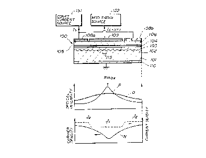
Referrlng to Eigure 5A showing a longitudinal cross-
sectlonal view, the DFB laser diode of the first embodiment,
represented generally by a numeral 100, includes an n-type InP
substrate 101 and a wavegulde layer 103 provided thereon. The
waveguide layer 103 may comprlse a GaInAsP layer having a layer
thickness d of about 0.1 ~m and an electro-luminescence ~EL)
wavelength ~g corresponding to the band gap energy of about 1.3
~m. The layer 103 may be doped to the n-type with an impurity
concentration level of 5 X 1017 cm . ~ :
As illustrated in the cross-sectional view of Figure SA,
there is formed a corrugation or diffraction grating 102 havlng a
pitch of about 2400 A and a depth of about 300 - 400 A. Further,
~here ls formed a phase shift region 115 in the diffraction
grating 102 generally in correspondence to the center thereof such
that the phase of the corrugatlon is shifted by a quarter of the
wavelength of the corrugatlon forming the diffraction gratlng 102.
As will be described later, thi3 phase shift region 115 acts to
induce an unhomogeneous distribution of the optical radiation in
an active layer 104 such that there appears a maxi~um of the
intensity of the optical radiation in correspondence to the phase
shift region 115.
On the waveguide layer 103, there 16 provided the
foregoing active layer 104 with a thickness of about 0.1 ~m. The
21~36~
- 16 - 27879-31
aative layer 104 comprises an undoped GaInAsP layer and has an EL
wavelength Ag o~ about 1.55 ~m. The actlve layer 104 and the
waveguide layer
:' ~ :,',,~
'.. -.'.,.. '.~" .",':','' ' .'
213~3~2
- 17 -
1 103 form a resonator structure 103a. Further, in order
to protect the active layer 104, an anti-meltback layer
105 of a p-type GaInAsP, doped to an impurity
concentration level of 5 X 10l7 cm 3 and having an
EL wavelength ~g of 1.3lum, is provided with a
thickness of 0.06 ~m. Further, a clad layer 106 with a
thickness of about 1 - 2 ~m of a p-type InP layer having
an impurity concentration level of 5 X 1017 cm 3 is
provided on the anti-meltback layer 105.
Further, an n-type ohmic electrode 110 of
gold-germanium/gold structure is provided on a bottom
surface of the substrate 101 for making an ohmic
contact. On the clad layer 106, a contact layer 107 of
p -type GaInAsP having an impurity concentration level
of 1 X 1019cm 3 is provided with a thickness d of
0.2 ~m such that the contact layer 107 is divided into
three distinct segments, one (107a) in correspondence to
an end of the structure 100, one (107b) in -
correspondence to the phase shift region 115 and one
(107c) in correspondence to the other end of the
structure 100. Further, a first segmented electrode
108a, a second segmented electrode 109 and a third
segmented electrode 108b are provided respectively on
the segmented contact layers 107a - 107c so as to form
an ohmic contact therewith. Further, an anti-reflection
film 111 is provided at both ends of the DFB structure
100. This anti-reflection film 111 may comprise a thin
film of silicon nitride having a thickness of about 2000
A which is about one quarter of the oscillation
wavelength of the laser diode.
FIG.5B shows a transversal cross-section of
the laser diode structure 100. As can be seen from
FIG.5B, the waveguide layer 103, the active layer 104
and the anti-meltback layer 105 on the top of the active
layer 104 form a mesa structure, and both sides of the
mesa structure are supported by a pair of p-type InP
layers 112. In other words, the laser diode 100 has a
21 3~362
~ 18 -
1 buried structure wherein the mesa structure including
the waveguide layer 103 and the active layer 104 is
laterally bounded by the p-type InP layers 112 and
vertically bounded by the clad layer 106 and the
substrate 101. Further, a pair of n-type InP buried
layers 113 are provided within the p-type InP layer 112
such that the buried layers 113 are opposite to each
other at both sides of the mesa structure. Further, an
insulator layer 114 of silicon oxide and the like is
provided on the top surface of the clad layer 106 such
that drive currents are injected into the active layer
104 via respective segmented electrodes 108a, 108b and
109.
In such a structure, the carriers injected
through the segmented electrodes 108a, 108b or 109 and
flowing towards the electrode 110 at the bottom of the ~ ~ :
substrate 101 are confined laterally into a path which
passes through the active layer 104 because of the
depletion region (not shown) formed in correspondence to
the p-n junction extending along the boundary between
the p-type InP layer 112 and the n-type InP layer 113
and an ~ffective injection of the carriers into the
active layer 104 is achieved.
As the active layer 104 has a refractive index - :
25 which is higher than the refractive index of the : :
semiconductor layers 103, 105, 106, 112 or 113 -
surrounding the active layer 104, the optical radiation ~:
formed in the active layer 104 as a result of ~.
recombination of the carriers is confined within the
active layer and the intensity of the optical radiation
becomes maximum in the active layer 104.
In the DFB laser diode wherein the laser
oscillation is caused as a result of the Bragg
reflection of optical waves by the diffraction grating,
there is a tendency that the intensity of the optical
radiation assumes a maximum generally in correspondence ~ ~ :
to the center of the diffraction grating or resonator
2~31 362
-- 19 --
l which extends along the longitudinal direction of the
laser diode. This is because the optical beams
propagating in one direction after a reflection by the
diffraction grating and the optical beams propagating in
another, opposite direction after a reflection by the
diffraction grating interfere most strongly at the ~ ~:
center of the diffraction grating which coincides with ~ :
the center of symmetry of the diffraction grating. :
In the present invention, there is provided
lO the foregoing phase shift region 115 generally in -~
coincidence with the center of the diffraction grating
102. By forming the region 115 as such, there exists a
strong optical radiation in the resonator structure 103b
at the region 115 coinciding with the center of symmetry
as already described, while at the positions offset from
the region 115, the intensity of the optical radiation
is decreased significantly because of the loss of
sym~etry. More specifically, at a first region of the .
diffraction grating with respect to the phase shift
region, the condition of forming a strong Bragg
reflection by the interference of the optical radiation
formed in the first region and the optical radiation
formed in a second region at the opposite side of the
phase shift region 115 and coming into the first region
across the phase shift region 115 is lost because of the
change in the optical path occuring at the phase shift
region 115. It should be noted that the phase of the
corrugation forming the diffraction grating at one side
of the region 115 is shifted with respect to the phase
of the corrugation in the other side by ~4 where a is
the wavelength of the corrugation forming the
diffraction grating 102. FIG.6 shows the distribution ~ :
of the optical radiation in the resonator structure 103a
including the active layer 104 in the case where the ~:
phase shift region 115 is not provided and in the case
where the phase shift region 115 is provided .
respectively by a curve 0 and a curve P. As can be seen
.
: ~
2~3~ ~2
- 20 -
1 in FIG.6, there appears a distinct peak in the intensity
of the optical radiation in the resonator structure
103a. In other words, the phase shift region 115 acts
as a means for concentrating the intensity of the
optical radiation formed in the resonator structure 103a
in a limited region.
In the present embodiment, the segmented
electrode 109 is provided in correspondence to the phase
shift region 115 where the intensity of the optical
radiation is maximum while the other segmented
electrodes 108a and 108b are provided respectively in
correspondence to the region where the intensity of the ,,~
optical radiation is minimum. Each of the segmented
electrodes 108a, 108b and 109 has a structure wherein a
titanium layer, a platinum layer and a gold layer are
stacked consecutively and makes an ohmic contact with
the underlying contact layer 107 as already described.
As illustrated in FIG.6, a drive current Is is supplied
from a constant current source 151 to the segmented
electrodes 108a,and 108b for driving the laser diode and
a drive current Ic is supplied from a modulation signal
source 152 together with a modulation signal i(t) ' ~
superposed on the drive current Ic. ' ''
Next, the operation of the DFB laser diode of
the present invention will be described with reference
to FIG.6.
Referring to the drawing, there is formed a
peak Pmax in the distribution of the optical intensity P
in the resonator structure 103a as already described.
30 In such a case, the carriers in the active layer lû4 are ,, ,
consumed most strongly in the region where the intensity
of the optical radiation assumes the maximum because of
the facilitated recombination of the carriers. In
FIG.6, such a distribution of the carriers is
illustrated by a curve N. It can be seen clearlj,v that
the curve P is inversely proportional to the curve N. '
By choosing the drive current Ic such that '
2~313~2
- 21 -
1 there occurs the intensity distribution of the optical
radiation as such, the carrier density changes
significantly in the active layer 104 immediately below
the electrode lO9 in response to the modulation signal
i(t) superposed on the drive current Ic, and in
correspondence thereto, there is a change in the
refractive index in the active layer 104 of a large
magnitude. In other words, the wavelength of the laser
oscillation can be changed significantly in response to
the modulation signal i(t) overlapped on the drive
current Ic and an efficient frequency modulation can be
achieved.
When the carriers are injected into the region
of the active layer 104 where the intensity of the
optical radiation is the maximum and the carriers are
strongly depleted, the carrier density is changed
significantly even when the injected current is small.
Thereby, the change in the threshold carrier density
explained previously with reference to the prior art
laser diode of FIG.3 is caused qulte effectively and the
foregoing large shift of the oscillation wavelength is
obtained. Particularly, when the current Ic is
increased so as to supply the carriers to the region
where the carriers are strongly depleted, the threshold
carrier density of the laser diode is decreased and the
oscillation wavelength is increased in response
thereto. Such an increase of the oscillation wavelength
occurs in the same sense as in the case of the thermally
induced modulation effect. Therefore, an increase in
the range of the frequency shift is achieved in the low
frequency range of the modulation signal while in the
high frequency range of the modulation signal, a flat
modulation characteristic is obtained.
In the case where the current Is is increased, -~
on the other hand, the non-uniform distribution of the
carriers is further enhanced and associated therewith,
the threshold carrier density is increased and the
': ~:'- "' '-' ':,. ',
213~2
- 22 -
1 overall number of the carriers in the active layer is
increased also. Thereby, the oscillation wavelength of
the laser diode is decreased. As the direction of shift
of the oscillation wavelength in this case is opposite
to the case where the shift is caused by the thermally
induced modulation, the change in the oscillation
wavelength in response to the change in the threshold
current density cancels out with the change caused by
the thermally induced modulation and no substantial
change occurs in the oscillation wavelength. In any
case, the magnitude of change of the oscillation
wavelength is small in this case, as the injection of
the carriers is made into the region where there are
already sufficient carriers.
In the present embodiment, it is preferred
that the current density designated as Jl formed in the
active layer 104 in response to the injection of the
current Ic from the electrode 109 be set equal to or
smaller than the current density designated as J2 formed
in the active layer 104 in response to the injection of
the current Is from the electrode 108a or 108b. As can
be seen in FIG.6, the current density J1 appears in
response to the center of the active layer 104 and the
current density J2 appears in response to both ends of
the active layer 104. By setting the current density J1
and the current density J2 as such (Jl ~ J2) in the
unbiased state where there is no modulation signal i(t)
applied to the electrode 109, the efficiency of ;
frequency modulation in response to the application of
the modulation signal i(t) can be maximized. It should
be noted that, by setting the carrier density J1 to be
smaller than J2, the carriers to be injected into the
region where the depletion of the carriers has occured
are further reduced. Thereby, a small change in the
carrier density cause a large change in the oscillation
wavelength and the efficiency of modulation is ;~
increased. Further, as the laser diode is operated in
. ~-
~3~3
,
- 23 -
1 the state that there i5 a gain in every regions in the
resonator structure 103a, a resonant phenomenon occurs
between the carriers and the photons and thereby a
modulation with a signal having a frequency of more than
10 GHz can be achieved.
In contrast, in the case of the conventional
DFB laser diodes having, for example, a plurality of
electrodes shown in FIG.3, the electrodes are provided
without particular consideration with regard to the
distribution of the optical intensity in the resonator
and thus, the electrodes do not generally correspond to
the maximum or minimum of the intensity of optical
radiation. Thereby, the modulation caused by the change
in the carrier density and the modulation caused by the
thermally induced modulation effect are cancelled with
each other to a considerable extent. Further, the DFB
laser diode of FIG.3 is driven such that the laser
oscillation is sustained by injecting a sub-threshold
level modulation current through the electrode 206a for
modulating the refractive index in the corresponding
part of the active layer while injecting the drive
current needed for the laser oscillation through the
electrode 206b. Thus, there is caused no significant
maximum in the distribution of the intensity of optical
radiation, but instead, a nearly uniform distribution is
obtained as shown in FIG.3, contrary to the case shown
in FIG.6. In the foregoing conventional laser diode
having the segmented electrodes shown in FIG.3, although
the efficiency of frequency modulation may be improved,
there arises a problem in that the fre~uency response is
limited by an upper limit frequency of about 1 GHz
corresponding to the lifetime of carriers for the
spontaneous emission as shown in FIG.7 by a continuous
line designated as PRIOR ART.
FIG.7 shows the efficiency of modulation
achieved by the DFB laser diode of the present
embodiment in comparison with the prior art DFB laser
2~313~2
- 24 -
1 diodes shown in FIG.2B and FIG.3, wherein the continuous
line beariny the label "PRIOR ART" represents the result
for the case of the laser dlode of FIG.3 and the broken
line bearing the label "PRIOR ART" represents the result
for the case of the laser diode of FIG.2B. The
continuous line designated as "THIS INVENTION"
represents the modulation achieved by the laser diode of
the present embodiment. As can be seen clearly from
FIG.7, the conventional laser diode of FIG.3 having two
electrodes shows a characteristic which drops steeply
when the frequency has exceeded about 1 GHz. In the
case of the laser diode of FIG.2B, on the other hand,
the efficiency of modulation is decreased in
correspondence to the intermediate frequency range
between 10 MHz and 100 MHz as already described. In
contrast, in the case of the present invention, a
sufficient efficiency is obtained up to the frequency of
about 10 GHz.
FIGS.8A and 8B are diagrams showing the output
characteristic of the system of FIG.6 in the case that
the current Ic and the current Is are changed, wherein
FIG.8A shows a case in which the current Is, supplied to
the segment electrodes 108a and 108b, is held constant
and the current Is supplied to the electrode 109 is
changed, while FIG.8B shows the case in which the
current Ic is held constant and the current Is is
changed. ;~
As can be seen from FIG.8A, there occurs a
large change in the oscillation wavelength generally in
proportion to the drive current in addition to the
change in the optical output power in the case that the
drive current Ic supplied to the electrode 109 is
changed. In the case that the current Is to the
electrode 108a or 108b is changed, on the other hand, ~ ;
there occurs little change in the oscillation wavelength
of the laser diode and only the output power of the
laser diode changes. In other words, in the system of
:::: ~:
~ ~ :
.~ - 25 _ U~
1 FIG.6, the output power of the laser diode can be
changed independently from the oscillation wavelength by
changing the drive current Is injected through the
electrodes 108a and 108b. By controlling the current Is
and the current Ic simultaneously, it is possible to
construct a system which p~oduces a frequency modulated
coherent optical beam with a constant optical output
power.
FIG.9 shows a system for producing a frequency
modulated coherent optical beam with a constant optical
output power.
Referring to FIG.9, the system includes, in
addition to the foregoing laser diode 100 and the
modulation signal source 152, a photodetector 154
provided at one side of the laser diode 100 for
detecting the output power of the laser diode and a
controller 153 for controlling the current Is in
response to the optical output from the laser diode
100. The controller 153 controls such that the current
Is is decreased in response to the increase of the
optical output of the laser diode 100 and such that the
current Is is increased in response to the decrease of ;
the optical output of the laser diode 100 based on the
detection by the photodetector 154.
As already described with reference ko FIGS.8A
and 8B, the optical output power of the laser diode 100
can be changed independently from the oscillation
wavelength by controlling the drive current Is. Thus,
the change in the output power caused in response to the
30 frequency modulation of the output optical beams can be i~
compensated for by the controller 153 by simply
increasing or decreasing the current Is in response to
the output power detected by the photodetector 154.
Thereby, the operation performed by the controller 153
can be simplified significantly.
FIG.10 shows a modification of the system of
FIG.9 in which a fixed power source 155 is used for
2~ 3~ 362
- 26 -
1 supplying a constant drive current Icl to the electrode
108a, and the controller 153 supplies a variable drive
current Is2 to the segmented electrode 108b. A feedback
control similar to the system or FIG.9 is made such that
the output optical power is monitored by the
photodetector and the current Is2 is changed by the
controller lS3 in response to the detected output
power.
According to the system of FIG.9 or ~IG.10,
the control of the oscillation wavelength and the output
optical power of the laser diode can be achieved
independently and the control performed by the
controller 153 for maintaining the output optical power
constant is significantly simplified.
15In the laser diode of the first embodiment, it
is preferable that the overall length of the resonator
structure 103a, which is defined as a distance L between
the pair of opposing anti-reflection films 111 in
FIG.5A, be set to about 500 ~m or more for achieving a
large frequency variation. By increasing the length of
the resonator beyond about 500~um, the proportion of the
light produced as a result of the stimulated emission as
against the proportion of the light produced as a result ~:
of the spontaneous emission is increased, and this
25 increasing of the length of the resonator is also -
responsible for the frequency shift of the laser
oscillation. Thereby, the range of frequency shift is
increased. As a result, the width of the spectrum of
the output optical beam can be decreased to about ~ MHz
or even several hundred MHz. Further, by increasing the
length of the laser diode beyond about 500 ~m, the heat
generated upon laser oscillation is effectively
dissipated. This feature is advantageous for increasing
the output optical power of the laser diode. In
addition to the foregoing, ordinary advantages
associated with the use of a longer resonator, the use -~
of the resonator with an increased length is
':
3 6 ~
-~ - 27 -
1 particularly preferable in the DFB laser diode of the
present invention, as such a laser diode having
resonator with an increased length shows a distribution
of the optical radiation along the longitudinal
direction of the laser diode such that a large
concentration of the optical radiation appears in
correspondence to the central part of the resonator.
This feature is particularly advantageous in the laser
diode of the present invention for increasing the
frequency range of the laser diode.
FIG.ll is a graph showing a relationship
between the length Lc of the segmented electrode 109 and
the variable range of oscillation frequency of the laser
diode. As can be seen in FIG.11, the frequency range
increases as the length Lc of the electrode 109
increases. In order to achieve a frequency range of
more than 100 GHz, it is desired that the ratio of the
electrode length Lc chosen with respect to the overall
length L of the resonator be more than 0.25.
It should be noted that the phase shift region
115 may be omitted from the laser diode 100 when the
laser diode can be constructed such that there is formed
a sufficient concentration of optical radiation in the
resonator structure 103a and when the electrode lO9 is ;~
provided in correspondence to the maximum of the
intensity of optical radiation. For example, when there
is a sufficiently sharp peak in the curve O which
represents the intensity distribution in the case where
the region 115 is not provided, the laser diode can
operate satisfactorily although there may be a
degradation in the efficiency of modulation. ';-~
Next, a second embodiment of the present
invention will be described with reference to FIGS.12A
and 12B showing a DFB laser diode 100' of the second
embodiment wherein FIG.12A shows a plan view and FIG.12B
shows a perspective cross-sectional view taken along a
line 12-12'.
21 313~2
- 28 -
1 Referring to FIG.12B at first, the DFB laser
diode 100' has a layered structure of the semiconductor
layers 101 - 107 similar to that of the first embodiment
except that there is provided a pair of grooves 141 at
both sides of the mesa structure such that the grooves
141 extend from the surface of the structure 100' and
reach the substrate 101. It should be noted that there
are a plurality of grooves 141 along the longitudinal
direction of the structure 100' respectively in
correspondence to the electrodes 108a, lO9 and 108b
wherein each of the grooves aligned along the
longitudinal direction is separated fro~ an adjacent
groove or grooves by a separation region 142. Further,
the surfaces of the grooves 141 as well as the top :~
surface of the contact layer 107 including the
separation region 142 are covered by an insulator film
114' which is formed with an opening 122 by which the
electrode 108a, 108b or lO9 comes into contact with the
contact layer 107. Each of the grooves 141 has a depth
20 of about 3 - 4 ~m and are disposed with a separation of :
about 10 - 20 ~m from each other in the lateral
direction, thus forming a second mesa structure between
the opposing grooves 141.
According to the present invention, the second
mesa region is isolated by the grooves 141 from the
region beyond the grooves 141 and thereby the influence
of the parasitic capacitance formed at the boundary :~
between the p-type layer 112 and the n-type region 113
is eliminated by the grooves 141. As the grooves are
separated from each other in the longitudinal direction
of the laser diode 100' by the separation regions 142,
the problem of unwanted conduction between the segmented
electrodes 108a, 108b and 109 which may occur because of
incomplete patterning when the grooves are continuous, :~
is positively prevented. As the separation region 142
forms an absorption region in the active layer 104 :~
because of the absence of carrier injection, it is
,.: ~ '; '~ :-
:. , :, . . .,:: ::. . ,:,, , :, , - . , : :
- ,,.:.: : ., . . : . :.:., : ... ~ ~ . ,
--2~ -~ 3 ~- 3 ~ 2
1 desirable that the length of the region 142 chosen to be
about 10 - 30 ~m. As a result of the foregoing
construction, a high speed modulation exceeding 1 GHz
and reaching about 10 GHz can be achieved with
reliability.
Next, the fabrication process of the DFB laser
diode of the present invention will be described with
reference to FIGS.13A - 13F.
Referring to FIG.13A, a buried structure of
semiconductor layers forming the laser diode 100 is
formed by stacking consecutively the n-type GaInAsP
waveguide layer 103, the undoped GaInAsP active layer
104, and the p-type InP clad layer 106 on the n-type InP '
substrate, selectively etching the layered structure
thus formed by using a suitable silicon oxide mask (not
illustrated) to form the mesa structure having a width
of 1 - 2 ~m, depositing the p-type InP layer 112 and the
n-type InP clad layer 106 consecutively to bury the mesa
structure together with ion implantation and following
annealing processes to form the buried layer 113 in
correspondence to the boundary between the layer 112 and -~
the layer 106, removing the silicon oxide mask, and
depositing the p type GaInAsP contact layer 107 on the
clad layer 106. Further, a photoresist 120 is deposited
25 on the contact layer 107 as shown in FIG.13A.
Next, the photoresist 120 is patterned in
accordance with the groove 141 to be formed in the
structure of FIG.13A and openings are formed in the
photoresist 120 as shown in FIG.13B.
Next, using the photoresist 120 as the mask,
the grooves 141 are formed by etching as shown in
FIG.13C and the surface of the groove 141 as well as the
top surface of the contact layer 107 is covered by the
silicon oxide film 114'. It should be noted that there
is formed another mesa structure by the pair of grooves
141 as shown in FIG.13C and FIG.13D. This second mesa
structure may typically have a width of 5 - 8 ~m.
2~-313~2 . .
- 30 -
1 Further, an opening 122 is formed in the silicon oxide
film 114' to allow for electrical contact between the
contact layer 107 and the electrode 108a, 108b or 109
provided thereon and a structure shown in FIG.13D is
formed.
Next, a titanium/platinum layer 161 is
provided on the silicon oxide film 114' uniformly as
shown in FIG.13E, and after providing a suitable resist
pattern (not shown) on the titanium/platinum layer 161
in correspondence to the groove 141, a
gold/germanium/nickel layer 162 is deposited on the
titanium/platinum layer 161. Thereby, a structure shown
in FIG.13E is formed. Next, the resist pattern is -
removed and the layer 161 is selectively removed by a
reactive ion etching process (RIEJ using the layer 162
as the mask. As a result, a structure shown in FIG.13F
corresponding to the cross section shown at the end of
the perspective view of FIG.12B is obtained. It should
be noted that the structure thus obtained has the
electrodes 108a, 109 and 108b which are segmented and
separated completely from each other as can be seen in
FIGS.12A and 12B.
It should be noted that the deposition of the
electrodes 108a, 108b and 109 can be made such that a
part of the electrodes extend laterally across the
grooves 141, thus filling the grooves without difficulty
by simply omitting the photoresist and etching process
at the time of deposition of the electrode layers 161
and 162. Thus, the laser diode formed with the grooves
30141 and having the electrodes 108a, 108b and 109 as ~ ~-
shown in FIG.12B is fabricated. As the grooves 141 are
segmented in the longitudinal direction, there is no
risk that the separation between the electrodes 108a,
: ::.:
108b and 109 will be not incomplete and a reliable
operation o~ the laser diode can be achieved.
In the laser diode fabricated as such, it
should be noted that grooves 141 are divided into
:
. .:- ., . ,i - . :.,., ,~, . , . " . ,
.. . ~ ~ ,, ., ... . ~ . , ,., .: ;... . . . . , :
2~313~2
- 31 -
1 segments in the elongated direction of the laser diode.
Thereby, the electrical separation between the segmented
electrodes 108a, 108b and 109 becomes complete and short
circuiting between the electrodes is positively
prevented. Further, the unwanted effect of the
parasitic capacitance is reduced by the provision of the
grooves 141 as already described.
Next, a description with respect to the mask
used for forming the grooves 141 by etching will be
made.
FIG.14A shows a typical example of the mask
used in fabrication of semiconductor devices for forming
grooves in a semiconductor structure and FIG.14B shows
: .
an example of the grooves formed by the mask of
15 FIG.14A. As will be noted in FIG.14B, the grooves 141
formed by using the mask having straight ends at the
ends of the openings 121, have enlarged ends which
appear as a result of the different etching rate in the
crystal orientation of the semiconductor crystal. As
20 the active layer 104 is formed between the grooves 141,
such enlarged ends of the grooves 141 may cause a
serious degradation in the efficiency of laser
oscillation. It should be noted that the width of the
active layer 104 is only about 1 - 2 ~m.
In the present invention, a mask shown in
FIGS.15A or 15B is used for forming the grooves 141
without the enlargement of the grooves at the end
thereof, wherein each of the masks has the opening 121
in which the width W of the opening is decreased
gradually towards the end of the grooves 141, in which
FIG.15A shows a case that the opening 121 has a curved
edge and FIG.15B shows a case that the opening 121 has a
straight edge. The length of the end region L in which
the width W is changed gradually may be chosen to be 4 -
5 times as large as the maximum of the width W.Alternatively, the grooves 141 may be formed by using
the mask of FIG.15C. In this mask, there is formed a
CA 02131362 1998-0~-13
- 32 -
pair of elongated openings 121' with a separation between them
which increases toward the end of the openings in
correspondence to the end region L. Thereby, the separation
between the openings 121' at the end thereof may be increased
twice as large as the separation x between the openings 121'
outside the region L. Using the mask as disclosed in
FIGS. 15A - 15C, one can obtain substantially straight grooves
141. FIG. 16 shows a plan view of the structure formed as a
result of the step of FIG. 13D. As can be seen in the
drawing, the grooves 141 are segmented or separated from each
other in the longitudinal direction of the laser diode 100'
and have an end part defined without any enlargement in
contrast to the conventional groove shown in FIG. 14B.
Next, the process of forming the phase shift region
115 in the diffraction grating 102 will be described briefly
with reference to FIG. 17. A more complete description will
be found in an article by Shirasaki et al. (M. Shirasaki, H.
Soda, S. Yamakoshi and H. Nakajima, " A/4-shifted DFB-LD
Corrugation Formed by a Novel Spatial Phase Modulating Mask",
5th International Conference on Integrated Optics and Optical
Fiber Communication, 11th European Conference on Optical Fiber
Communication (IOOC-ECOC'85), Venetia, Italy, October 1 - 4,
1985, Technical Digest Vol. 1, pp. 25 - 28).
Referring to FIG. 17, a pair of laser beams from an
argon or helium-cadmium laser are irradiated on the substrate
101 coated by a photoresist with two mutually different angles
of incidence ~L and ~R through a transparent phase plate 180
27879-31D
CA 02131362 1998-0~-13
- 32a -
of quartz which is provided with a step H of 2.2 ~m in
correspondence to where the phase shift region 115 is
provided. It should be noted that the optical path of the
laser beam incident to the plate at the left of the step H is
different from the optical path at the right of the step
27879-31D
2~3~3~
- 33 -
1 H, and as as a result, there appears a shift of the
regularly repeated inter~erence bands, which are formed
on the photoresist as a result of the interference of
the two laser beams, in correspondence to the step H.
After the foregoing exposure of the photoresist, the
substrate 101 is patterned using the exposed
photoresist, and a corrugation including the phase shift
of ~ 4 corresponding to the phase shift region 115 is
formed on the substrate 101 as the grating 102 as shown
10 in FIG.17. ~ -
Next, a third embodiment of the present
invention will be described with reference to FIG.18.
In FIG.18, the parts corresponding to those already
described with reference to the preceding drawings will ~ ~'
be designated by the same reference numerals and the
description thereof will not be repeated.
Referring to FIG.18, the DFB laser diode has
two phase shift regions 115a and 115b generally in -~ j
correspondence to the gap between the electrodes 108a
~0 and 109 and the gap between the electrodes 109 and 108b,
respectively. Thereby, there appears two peaks in the
intensity distribution of the optical radiation
established in the resonator structure 103a and in
correspondence to this, the intensity of the optical
radiation under the electrode 109 is increased
uniformly. More specifically, the intensity of the peak
Pmax of the optical radiation has a width corresponding
to the electrode 109 and the efficiency of modulating
the oscillation wavelength in response to the modulation
signal applied to the electrode 109 is improved. In
other words, a large shift of the oscillation wavelength
of the laser diode can be achieved by the structure of
FIG.18. It should be noted that the location of the
phase shift regions 115a and 115b may be chosen such
that there appears the maximum Pmax with a width
generally corresponding to the electrode 109 and with a
sufficient height, and the location is not limited to
, . . . . . . .. .. . . . . . .
34 ~31362
1 the location corresponding to the gap between the
electrodes 108a and 109 or the gap between the
electrodes 109 and 108b.
Next, a fourth embodiment of the DFB laser
diode of the present invention will be described with
reference to FIG.19.
In the embodiments described heretofore, the
unhomogeneous distribution of the intensity of the
optical radiation in the resonator structure 103a is
10 artificially induced by the phase shift region 115 in -
the diffraction grating 102 as already described. In
such a structure, there is a tendency that a laser
oscillation of secondary mode is induced such that the
intensity of laser oscillation is strongest at the ends ~ -
of the resonator structure 103a and weakest at the
center of the structure 103a. As such an oscillation
mode is insensitive to the modulation signal applied to
the electrode 109, it is desired that the intensity of
laser oscillation in this secondary mode be suppressed
as small as possible.
The structure of FIG.19 is designed to
..
eliminate or suppress the unwanted secondary mode.
Referring to FIG.l9, the depth of the corrugation
forming the diffraction grating :L02 is changed such that
the depth of the diffraction grating is small at end
parts Ll of the resonator structure 103a while the depth
is large at the central part Lc of the resonator
structure. Thereby, the quality factor Q of the
resonator structure 103a is reduced in correspondence to
the end parts thereof and the oscillation of the
secondary mode having a large amplitude at the end parts
of the resonator structure is effectively suppressed.
At the same time, the primary mode having a large
amplitude in correspondence to the central part of the ~
35 resonator structure is effectively enhanced as shown in ~ -
the lower part of FIG.19.
Next, a fifth embodiment of the present
: : . ,. : : .. ::::.- ::. : ~ . :.. :: : . :
2~.3:13~2
- 35 -
1 invention for providing a fla~ and strong intensi-ty o~
optical radiation in the part of the resonator structure
103a underneath the electrode 109 and a flat and weak
intensity of optical radiation in correspondence to the
part underneath the electrodes 108a and 108b together
with the effective suppressing of the secondary mode,
will be described with reference to FIG~.20A and 20B.
Referring to FIG.20A, there are provided a
plurality of phase shift regions 115a, 115b and 115c
underneath the electrode 109 and associated therewith,
an intensity distribution designated as PRIMARY MODE in ~-
FIG.20B is established in the resonator structure 103a.
Further, the depth of the corrugation forming the
diffraction grading 102 is changed as shown in FIG.20A
such that depth of corrugation is reduced in
correspondence to both ends L1 of the resonator
structure 103a and in correspondence to the center L3 of
the structure 103a underneath the electrode 109, while
the depth of corrugation is in~creased relatively in the
intermediate region L2 as compared to the region L1 or
region L3. By reducing the depth of corrugation at both
ends of the resonator structure 103a, the coupling
constant which represents the degree of interaction
between the optical waves and the grating is reduced.
In other words, the quality factor Q of the resonator in
this region is reduced and the secondary mode laser
oscillation having the maximum intensity in
correspondence to this region is substantially reduced.
On the other hand, the reduced corrugation depth at the
central part of the electrode 109 contributes to flatten
the sharp peak of the optical intensity in this
region.
Next, the fabrication process of the
diffraction grating 102 which is used in the embodiment
of FIG.20A will be described with reference to FIGS.21A
- 21E.
Referring to FIG.21A, a negative photoresist
: . . ~ . , ~ . . .. i . : : .
2131362
- 36 -
1 181 is deposited on the substrate 101 and patterned in
accordance with an 1nterference pattern of an argon or
helium~cadmium laser defining the diffraction grating.
During this process, the phase shift plate 180 as shown
in FIG.17 may be used.
Next, in a step shown in FIG.2lB, the
substrate 101 is etched slightly using the negative
photoresist 181 as the mask, and in a step of FIG.21C, a
positive photoresist 182 is deposited in correspondence
to the region where the depth of corrugation has to be
shallow.
In a step of FIG.21D, the substrate 101 is
subjected to a further etching process wherein the part
of the substrate lO1 which is not protected by the
photoresist 181 or by the photoresist 182 is grooved
deeply as illustrated. After removal of the photoresist
181 and 182, the structure shown in FIG.21E having ~ -~
different corrugation depths is obtained.
FIGS.22A - 22F show alternative steps for
forming the diffraction grating 102 with different
corrugation depths.
Referring to FIG.22A, the substrate 101
carrying the negative photoresist 181 is patterned
according to the diffraction grating 102, and the
positive photoresist 182 is deposited selectively in a
step of FIG.22B so as to protect the region where the
depth of corrugation is to be reduced.
Next, in a step of FIG.22C, the exposed part
of the substrate 101 is grooved by etching and in a step
of ~IG.22D, the positive photoresist 182 is removed.
Thereby a structure, partially etched and protected ;
selectively by the negative photoresist 181 is
obtained. -~
By applying the etching process again, there
35 are formed deep corrugations in the region which has ~ ~ -
already been etched and shallow corrugations in the
region which has been protected by the positive
~ '
~ 213:L3~2
- 37 ~
1 photoresist 182 as shown in FIG.22E. By removing the
photoresist 181, the diffraction grating 102 in which
the depth of the corrugation is changed is obtained as
shown in FIG.22F.
Next, a sixth embodiment of the DFB laser
diode of the present invention will be described with
reference to FIGS.23A and 23B. In the drawing, the
parts corresponding to those which have been described
previously with reference to the preceding drawings will
be given identical reference numerals and the
description thereof will be omitted.
Referring to FIG.23A showing the structure,
the diffraction grating 102 of the laser diode is formed
such that the corrugation is entirely eliminated from
the central region Lc of the grating 102 immediately
underneath the electrode 109. In response to the
elimination of the corrugation from the region Lc, the
sharp peak of the intensity distribution of the optical
radiation in this region is flattened and a distribution ~ -
profile of the optical radiation intensity as shown in
FIG.23B is obtained. It should be noted that there
appears sufficient concentration of the optical
radiation in this region because of the reflection from
the corrugations forming the diffraction grating at both
sides of the region Lc. As the high optical intensity
exists in correspondence to the entire region Lc, the
efficiency of modulation in response to the modulation
signal applied to the electrode 109 is significantly
improved.
Although the present invention has been
described heretofore with the structure wherein the
waveguide layer is provided between the substrate and
the active layer, with the diffraction grating formed at -
an interface between the active layer and the waveguide
layer, the present invention is by no means limited to
such embodiments but the wave guide layer may be
provided on the upper side of the active layer or at ~;~
.' :
~3~2
38 -
1 both sides of the active layer. Associated therewith,
it should be noted that the diffraction grating may be
provided along the top surface of the active layer.
Further, the waveguide layer may be provided with a
separation from the active layer as long as there is an
optical interaction between the active layer and the
waveguide layer such that the optical radiation formed
in the active layer is transferred to the waveguide
layer. In this case, the diffraction grating is
provided not on the top or bottom surface of the active
layer but with a separation from the active layer.
Further, the present invention includes in the scope
thereof the case in which the active layer has the ~ .
multiple quantum well (MQW) structure in which a number
of thin acti.ve layers with a thickness reduced to form a
quantum well therein are sandwiched by a number of
barrier layers providing the potential barrier defining
the quantum well.
Further, the present invention is not limited
to the embodiments described heretofore but various
variations and modifications may be made without
departing from the scope of the invention.
;