Note: Descriptions are shown in the official language in which they were submitted.
2132825
Process for Coating a Substrate with a Material Giving a
Polished Effect
The present invention relates to a process for coating a
substrate with a material, such as a metal, giving a
polished effect, the substrate being of a suitable material
that is dimensionally stable at temperatures of up to at
least 120°C.
In order to achieve the effect of a high polish on object,
according to the prior art electroplating with chromium,
nickel, or anodizing are used. When this is done, costly
pre-treatments of the base material, such as surface
polishing, are required in order to achieve the desired
effect of a high polish. Further-more, some materials cannot
be given a lasting high-lustre metallic finish, as in the
case, for example, of chromium on aluminum. In addition,
certain processes also entail the disadvantage of
contributing to considerable environmental damage.
It is known that PVD or CVD processes can be used in
conjunction with a wet-lacquer technique in order to achieve
metallizing, although the required durability cannot be
achieved in those areas that are endangered by corrosion.
The mechanical and chemical stability of wet lacquers is not
sufficient for coating parts that are highly stressed. Very
frequently, corrosion protection leaves a great deal to be
desired, and wet lacquering also gives rise to environmental
hazards.
DE 33 33 381 A1 describes a process for producing a metallic
coating on a base layer that is extremely weather-resistant
and is of a binary polyurethane coating or a UV hardenable
~~~~82~
coating, using dry plating such as sputtering and the ion
plating, and production of a top coating by applying a
binary polyurethane lacquer or a W hardenable lacquer that
is highly weather-resistant to the metal coating. The
process relates only to shaped bodies that are of plastic.
In order to achieve a metallic lustre, it is essential to
apply a base coating of a binary polyurethane coating or a
W hardenable coating to the surface. Coloration is
provided either by the body itself or by the base coating.
It is the task of the present invention to describe a
process of the type described in the introduction hereto, by
which high-lustre metallizing can be achieved without
causing any environmental damage, and by which almost any
desired geometry can be achieved at a consistent quality.
This problem has been solved by a process that comprises the
following steps:
a) Cleaning of the substrate;
b) Coating the cleaned substrate with the material giving
the polished effect in a vacuum chamber, within which a
plasma process is carried out;
c) Application of a powder lacquer coating as a top
coating andburning this on,
and, according to the present invention, by the following
process steps:
a') Burning on and incorporating a powder lacquer coating
as a base coating on the substrate;
- 2 -
CA 02132825 2004-09-27
b') Coating the base coated substrate with the metal that
gives the polished effect within a vacuum chamber
within which a plasma process is carried out;
c') Application of a powder lacquer coating as a top
coating and burning this on.
According to one aspect of the present invention, there is
provided a process for coating a substrate with a metal
giving a polished effect, the substrate being dimensionally
stable at a temperature of at least 120°C, comprising the
steps of (a) cleaning the substrate, (b) coating the
cleaned substrate with the metal giving the polished effect
by plasma deposition in a vacuum chamber, and (c) coating
the metal coated substrate by burning on a powdered lacquer
to form a top coating.
According to a further aspect of the present invention,
there is provided a process for coating a substrate with a
metal giving a polished effect, the substrate being
dimensionally stable at a temperature of at least 120°C,
comprising the steps of (a) forming a base coating on the
substrate by burning on a powdered lacquer, (b) coating the
base coat on the substrate with the metal giving the
polished effect by plasma deposition in a vacuum chamber,
and (c) coating the metal coated substrate by burning on a
powdered lacquer to form a top coating.
A powder lacquer coating is used as the base coating, and
this is burned on at a substrate temperature of 120 to
240°C; this burning-in lasts for approximately 8 to 30
minutes.
3
CA 02132825 2004-09-27
As a consequence, according to the present invention, it is
possible to coat substrates that do not exhibit. any
deformation in the above-cited temperature range. Such
substrates can be of metal, ceramic, glass, plastics, and in
particular fibre-reinforced plastic.
The application of the base coat ensures that t:he substrate
surface is flat, i.e., that rough surfaces can be
"metallized" without any mechanical processing; the powder
lacquer coating that is to be burned on smooths the surface
in such a way that any rough spots the were originally
present are covered over.
The powder is preferably a polyester resin compound, with
deposition onto the surface being effected
electrostatically.
After that, the material that gives the polished effect is
applied by the plasma process. Aluminum, chromium,
titanium, silver, and gold are examples of suitable
materials. To this end, the substrate is placed in a
reaction chamber, in which the pressure is initially at
3a
2132825
least 10 4, preferably 10' to 10 5 millibar. This means
that, in particular, oxygen and nitrogen molecules are
removed to the required extent. The reaction chamber is
then flooded with a grocess gas (inert gas or reactive gas)
until the pressure is between 1 millibar and 10-3 millibar.
Finally, a glow discharge is triggered, and a plasma
results. The material that gives the desired polished effect
is then vapourized in this plasma, so that the vapourized
metal is deposited onto the substrate that is in the plasma.
The required plasma can be generated either within the
reaction chamber by building up an electrical field between
an anode (recipient) and a cathode (substrate) by means of
DC current or high frequency (kHz - MHz, preferably 13.56
MHz), or outside the reaction chamber by a high-frequency
field (GHz, microwave).
If the plasma is generated by high frequency, it must be
ensured that the substrate surface is smaller than the
recipient surface in order to ensure sufficient polarization
of the electrodes.
The coating can also be effected by means of an arc
vapourizer, a laser vapourizer, or by cathodic sputtering
(single or double cathode). If this type of coating is
used, separate generation of the plasma is eliminated, for
the plasma is generated by the vapourizing or sputtering
process.
After metallizing, a protective coating can be formed in an
intermediate step, for example, by plasma polymerization,
and the top coating is applied to this. This top coating is
- 4 -
-~ 21~~82~
comparable to the base layer with respect to structure and
production, i.e., in that a powder consisting preferably of
a polyester resin compound is deposited electrostatically
and then burned on at a temperature range between 120°C and
240°C for a period of 8 to 30 minutes.
Finally, a scratch-proof protective coating can be applied,
this consisting preferably of a carbon compound.
Additional details, advantages, and features of the present
invention are set out not only in the claims that describe
these features, but also from the following description on
an embodiment that is shown in the drawings appended hereto.
These drawings show the following:
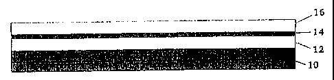
Figure 1: a coating structure of a material giving a
polished effect;
Figure 2: A process diagram;
Figure 3: A diagram illustrating the principles of a plasma
chamber.
A powder of a polyester-resin compound is applied electro-
statically to a substrate (10) that can be of any geometry,
and then burned on at a substrate temperature of
approximately 120°C to 240°C for a period from 8 to 30
minutes, in order to produce a base coating (12) that is
- 5 -
2~3282~
from 25~ to 125 thick. This ensures that any surface
roughness of the substrate (10) that was originally present
is smoothed out. Alternatively, or in addition, the surface
of the substrate (10) can be cleaned.
The substrate (10) can be of any material, such as metal,
ceramic, glass, or plastics, providing that the secondary
requirement, that the required dimensional stability is
maintained at the burn-on temperature that is used, be
Satisfied.
Then, the substrate (10) with the base coat is placed in a
reaction chamber that is initially set at a pressure that is
between 10 4 and 10 5. In this way, oxygen and nitrogen
molecules, which could possibly lead to undesirable
reactions, are removed.
Next, the reaction chamber is flooded with a process gas,
preferably argon, when a final pressure between 1 and 10 3
msllibars is set.
In order to achieve a high-lustre effect on objects,
according to the prior art, electroplating using chromium or
nickel, or anodizing, are used. When this done, costly pre-
treatments of the base material, such as surface polishing,
are needed in order to arrive at the desired high-lustre
effect. In addition to this, certain materials cannot be
metallized to give a high lustre that is lasting; this is
the case, for example, with chromium on aluminum. In
addition, such procedures also entail the disadvantage that
they can give rise to environmental damage.
- 6 -
rvle3w~we)
A metal such as aluminum, chromium, titanium, silver, or
gold is vapourized in the plasma that is formed, in order to
coat the substrate (10) that is in the reaction chamber,
which is to say, to provide the base coating (12) or the
substrate that has been cleaned with the coating (14) that
gives the polished effect.
Once the coating (14) has been applied, in a subsequent step
of the process a top coating (16) is applied by means of
electrostatic powder coating; when this is done, the process
sequence corresponds to the one that results in the
formation of the base coating (10). The top coating (16)
should also be between 25~ and 125. thick. The top coating
provides for good mechanical and chemical resistance.
In this way, the thickness of the coatings (12), (14), and
(16) amounts to a total of approximately 50~ to 250..
In order to vary the polished effect to the extent that is
desired, a matt or glossy powder lacquer can be used as the
base coating (12) or the top coating (16), and this has to
be clear transparent to colours for the top coating (16).
If so desired, a final coating (not shown herein) can be
applied in an additional process step, this consisting of a
carbon compound that is highly resistant to scratching.
Figure 2 is a process diagram for a continuous system for
coating shaped bodies such as rims, for example.
The shaped body (substrate (10)) is cleaned and degreased in
a pretreatment zone (18), so that it can be subjected to
~132~2J
conversion treatment. This is followed by drying with hot
air. Then the shaped body (10) is moved into powder cabin I
(20) in which the base coating (12), preferably a powder
lacquer coating, is applied automatically. This application
of the powder lacquer coating in the powder cabin I can be
carried out electrostatically.
After leaving powder cabin I (20) the shaped body (l0) is
moved into oven I (22), within which it first passes through
an infrared zone in order that the shaped body is heated to
a desired substrate temperature, e.g., in the range from
200°C to 220°C.
Once the base coating (12) has been burned on, [the shaped
body (10)7 passes through a high-vacuum multi-chamber
continuous system (24) that, in the embodiment shown,
comprises the chambers (26), (28), and (30). The chamber
(26) is an input buffer, and the chamber (30) is an output
buffer. The actual application of the material that gives
the polished effect is made in chamber (28), it being
preferred that this be done by plasma vapourization.
After leaving the chamber (30), the shaped body (10) is
moved to powder cabin II (32), in which a top coating (16)
in the form of a powder lacquer coating is applied,
preferably by electrostatic deposition. It then passes
through oven II (34) that incorporates an infrared zone (36)
and a burn-on zone (38); within this oven, the object (10)
is heated to the desired temperature, e.g., to approximately
200°C to 220°C. The object (10) is then cooled so that it
can be removed from the system.
_ g _
CA 02132825 2004-09-27
The high-vacuum multi-chamber continuous system (24)
consists, for example, of the three vacuum chambers (26),
(28), and (30) that are of equal dimensions, and which are
separated from each other by locks (S1), (S2), (S3), and
(S4). The shaped bodies (10) first pass through the lock
(S1) into the input buffer (26). This is evacuated to the
pressure that is set in the process chamber (28). After it
has reached this pressure, the locks S2 and S3 are opened.
The body that is is the plasma chamber (28) now moves into
the output buffer (30) and the body that is in the input
buffer (26) moves into the process chamber (28). Next, the
locks (S2) and (S3) are closed. The input buffer (26) and
the output buffer (30) are now ventilated and then the locks
(S1) and (S4) are opened. The body (10) that has been
vapour-coated can now be moved out of the output buffer (30)
and the next body (10) can be moved into the input buffer
(26). Parallel to this, the body (10) that is in the plasma
chamber (28) is being vapour-coated.
The advantage of this system is that the cycle time is
brief, since there is always a vacuum within the process
chamber (28), and working processes such as evacuation,
ventilation, and vapour-coating can be carried out in
parallel.
Figure 3 illustrates the principle of the plasma chamber
(28). The plasma chamber comprises a housing (30) that is
grounded and in which the substrate (10) that :is to be
coated with the material that gives the polished effect is
arranged. The substrate (10) is located betwe<~n the
cathodes (32) that are connected to the negative poles of DC
sources ( 34 ) .
- 9 -
213225
Thus, plasma can form between the cathodes (32) and the
substrate (10).
The housing (30) can be connected to a vacuum pump by way of
a connector (36). The required process gas itself is
introduced through the connector (38).
- 10 -