Note: Descriptions are shown in the official language in which they were submitted.
93~2~6~02 1 3 2 9 7 1 PCT/U~93/~3146
C~MPACT ~ D EFFICIENT TRANSFOXMERLESS
POWER CONVERSION SY5TEM
Backqround of the invention
Disclosed is a new Transformerless Power
Conversion System ~TPCS) that allows a direct voltage
st~p-up or step-down o~ DC or AC power without th~ use of
~ magnetic core transformers. The operation is
: accomplished with so~id state switching devices,
lO capacitors, preferentially air core inductors and a
switch control system.~
The conversion and step-up from AC to DC and the
: inverse process can be impleme~ed with high efficiency
: and without the generation of harmonics. The transformer
15 el.~mina~ion in conjunction with high inversion freguency
:: ~
operation results in a low weight system without
trans~ormer core losses and third harmonic generation.
For high ratio DC to DC~trans~ormation the TPCS
transports the input charge directly to the output
2~0~without~requiring an AC link. The three distinct
operations~of charging, transformation, and energy
;dis¢harge~are typically in sequential order and allows a
:complete isoIat~ion between the inpu :and out~ut power
grids~ The TPCS~al~lows complete power:flow control and
25~ wi~h~it:~allows an improvament of power grid sta~ility. A
n~m~er~o:~ inteyra~ed T~CS modules can be con~igured to
per~orm~in a single system as a voltage transforma~ion:
tage,~ a power:~on~erter or inwerter,~a~ output
: regulator,~an AC phase ansle corrector as well as a fast
; 30~:power~inter~up~ion device.
The architecture is specifically suited for high
voltage DC power distribution sys~ems with AC to D~
conversion and step-up at the power~:station for HVDC
: transmission; DC to DC step down for DC d:istribution in
,
~ 35 place of AC; and final ~C to polyphase AC power
2132r~71
WOg3~20610 ~ . PCT/~S~3/03146
c~nversion near tha bulk power consumers.
Summary_of the Invention
This invention relates to transformerless power
conversion system that allows ~oltage transformation of
5 either DC or AC, conversion of AC to DC or inversion of
C to AC. The system allows voltage st~p-up or step-down
of either AC or DC without the use of a transformer. In
combination with the appropriate controI logic and solid
: state switching devices, highly regulated output can be
10 obtained at ~egawatt power;level with an efficiency
equivalent to~that of unregulated standard AC power
: transformations. :
DC-DC Tra~3fo~matio~ ~
: : In ~he prior art for DC to DC step-up the DC
15 needed to be first~converted to high frequency AC. The
voltage transformation was then performed with a
transformer:and~the~AC was then con~erted back to DC.
Thei~rans~ormer not~only adds to the system weigh~ hut is
the maj~or contributor~or~the reduction o~ efficiency. In
2~ adaition:scaling to high power and~high voltages of the
order o~ lOO~KY:~is impractical. With~my in~ention the
inp~t:charge is directly transported to the output with
:an~ef~ficisn~ intermed:iate electrical vol~age
transfarmation;process~.~ :No AC~to:AC:transformation is
25~required.~: :Transformer~s~wi~h its:~demanding volt-second
scaling, magnetic core:losses, cost,~weight, and large
volume reguiremen~ are com~pletely eliminated.
: AÇ~A~ Tra~formatio~
The standard AC power distribution system is based
30 on the ~oltage:transformation capability of iron core
transformers~operating~typically at:a low frequency of 50
or 60 Hz. These devices~are large, costly, and have a
~, :
~ ' ~
-~093/20610 2 1 3 2 ~ 7 1 PCT~US93/03146
~onstant voltage transfer ratio given by the turns ratio.
My invention eliminates the transformer and all its
constraints on the AC power distribution system by
transporting the input power~electrostatically to the
5 output with simultaneous regulation capability.
~C ~y~tem I~t~r~oDn~io~
~ To inter~onnect two independent and unsynchronized
:~ power systems it is presently necessary to convert the AC
to DC and back to AC with the correct phase and
10 frequency. My invent~ion allows the direct transfer of
power from one polyphase system to a second polyphase
system without the use:of a DC~link. I must emphasize
:~ that the DC to DC~link interconniction benefits of power
grid for stabi~ization;:is retained with my TPCS AC to AC
:15 transformation:interconnection.
The prior art of high power polyphase ~C
` rectificati;on results~:in substanti;al production of
harmonics on to the AC~input;. The réquired harmonic
filtering Gontributes~appreciably to the power
`2:0 ~distribution cost.~ With~my invention:the AC to DC
transforDation;~and~step-ùp eliminates~the transformer and
the~har~onics:~filtering.~ ~By operating~at a high TPCS
frequency:~only:small filters are:re~uired at the ~C input
and~:D~:output.
: 25::~D~ Pow~er~Di~tribution ~ ~ :
: To clear a~high voltags DC line~fault the present
art~requires the shut-down of the complete DC line on the
converter AC inp~ ~end~ As a result DC lines are
presently only èconomical1y`viable for long distance
::30~ point to point power transport and~:for independent system
: `interconnection;. ~In~contr~st my invention allows the
implementation o~a c~mplete DC distribution with dire~t
~ DC to DC step-down with the elimination of all the
: ~:: : :::
~ ~ ,
2132J7 1
WO93/20610 PCr/US93/03146,
- 4 -
problems associated with the AC distribution system.
Faults on a DC branch line can be simply cleared by
momentarily stoppi~g the inversion process. Disconnect
switches can t~en be opened or closed under no load
S conditions.
~: :
: V~ri~ble Output ~r~qu~Doy
: The prior art of variable output frequency is
complex and costly to implement. The cycloconverter is a
high power control system that can directly convert ~C
lO polyphase power from high frequency to lower frequency.
` If a 60 Hz source~is used, the cycloconverter output
frequency is typical;ly ~ariable from z ro to 10 Hz with
the higher end of the frequency spectrum limited to abouk
40% of the ~upp~y fre~uency. The resulting low-fxeguency
15 wave is compo~ed of se~ments of the original source
frequency. The~output voltage can be made to approach a
: sine~ wave quite~closely~. However large reactive power
a~d haxm~nics are:~generated. In~addition the output
voltage:is limited.~
20~ : : In ~o~trast my invention allows the efficient
gensration~o~ output~with variable fre~uency and variable
voltage;.~ he ~ontrolled~output fr~quency may be higher
or ~lower~han the:frequency of the power source. ~he
same;~statement~applies~for the output:~v~ltage control.
~5:~Most~:im]portantly~my ~PCS variable frequency/voltage
con~roller~does;~not~generate:harmonics, input waveform
di~tortion or reacti~e power. In addition the ou*put
,:~: ,frequency,~the output phase, and output power can be
controlled at an efficiency similar to that of a AC power
; ., ~
30 ~ransformer.: The;~phase rotation can:be changed on a
subcycle ime period with controlled voltage output for
optimum start~up, torque control or speed ~ontrol of
induction motors.~ Furthermore an efficient variable
frequency converter can be also run with straight DC
~,:
~: ~
,-~WO93/20610 213 2 J 7 1 PCT~US93/03146
input with egual efficiency and performance.
~e~ctiYe Po~er Regulator ana ~armonic Filt~rs
TPCS modules can be configured as a fast response
phase angle correction system and reactive power
5 regulator (~ARG~ as part of the ~oltage transformation
system or as a separately stand alone unit. With the
fast TPCS operating characteristics such a VARG can
; respond on th~ time scale of a fraction of an AC cycle.
~: ~ Not only can my inY2ntion regulate the reactive pDwer
: 10 flow continuously ~r~m zero to its maximum rating but
~: ; also can respond to:both~leading and lagging Phase angle
correction requirement.
The phase angle~correction is performed without
generating either harmonics or phase distortion. For
15 balanced polyphase gr~ids my VA~ configuration does not
require ~he ~torage of~energy for large duration of a
cycle~a~ is:normally~required for most opèrating systems.
My ~ARG has similar 'black box' char~cteristics as a
S~n~hronous~ Hotor,~running~without a mechanical load.
2~Q~ The~;maj~or differènce is~that TPCS:V.ARG has no moving
par~t,:is much more:~economical to run, has much higher
;:eff~iciency~ and~can response in a faster tim~-scale.
The TP~S ~ARG operational characteristics allow it
to:be programmed~as~a~stand~alone or as integrated~ctive
25~:;Harmonic Filters~(AHF)~, again with no substantial energy
storage re ~ irement~ This operation is possi~:e since
TP~S~can extract;the reactive and harmonic power (or
charge) from the low volta~e part of an ~C cycle and can
~: ~ reinject it into another phase that has a high voltage.
30 The TPCS ~ARG/AHF~can be programmed to neutralize several
~:: harmonic frequencies~simultaneously. My invention allows
; the elimination of the large capacitor and reactor energy
: storage as is the state-of-the-art ~approa~h 2S desaribed
:; by Malesani at all (Active Power Filter with Hybrid
21 3 ~ ~ r;J 3L
WO93/20610 PCT/US93/03146 .
Ener~y 5torage, in IEEE Trans.on Power Electronics. Vol.
6 No. 3, July l99l).
With ~he presen~ state-of-the-art of either AC to
DC rectification~or ~C load control, passive or active
5 filtering are required to neutralize the generated
harmonicæ. ~he TPCS on the other hand can perform this
function as efficiently without producing harmonic
distortions on the AC input grid.
Xf harmonics and reactive power is generated by
lO non-linear and reactive AC loads the TPCS ~Itransformer~
: is powering, the TPCS can efficiently neutralize ~hem as
: Iong as the harmonics are balanced on the AC output. The
,
TPCS active harmonic filtering and reactive power
generation is performed without large energy storage
:15 re~uirement in the form of either capacitor banks or
: large inductors. Furthermore the architecture of the
TPCS;harmonic filtering system is such that it can
~: respond to the requirement:of`harmonic filtering level
change in a:fraction~of a- cycle. ~ ~ ~
20~ :Brief:DescriPtion o5 the Drawin~s
ther objects and features of my in~ention and of
these~:embodiments~thereof will be better understood from
the~fol~lowing specification taken in conjun~tion with the
: annexed~d~awings~:and:tables of which:
2~5~ FIG. l~ is~a representation o~ the basic TPCS
architecture-:and:~ome:selected electrical waveforms for
an~AC to~AC~converter;~ ~
: . - ~
FIG. 2~is a typical~three stage TPCS DC to DC
~; ~ Yoltage step-up transformation cir~uit;
: 30 FIG. 3 is~a~ hree stage TPCS DC to DC voltage
:~` step-down transformation circuit;
: ~ : FIG. 4 is a four quadrant step-up and s~ep-down
~:~ TPCS configuration allowi~g power flow control in both
the forward and backward direction;
'
.,~WO93/20610 2 1 ~ ~ ~ q 1 PCT/US93/03146
FIG. 5 is a single phase three stage TPCS AC to AC
transformation circuit wi~h bi-directional control
capability and with phase inversion;
: FIG. 6 is a typical single phase three stage AC to
5 DC converter module with voltage step-down
trans~ormation;
FIG. 7 is a typical polyphase TPCS AC o DC
conversion system with three phase input;
; FIG~ 8 is a typical circuit of a three stage DC to
10 single phase AC inversion module with voltage step-down
rans~ormation; ~ ;
: FIG. g is~a typical polyphase TPCS VAR generator
and harmonics filtering system for a three phase grid;
: FIGo 10 is~the voltage, reactive current, and
15 power for a three phase grid;
FIGo~ 11 is a:simplifi~d electrical configuration
:for one TPCS module:in conjunction with an inductor for
magnetic energy storage and retrieval;
Table l are~th~parameters of a specific control
2:0:~sequence~for a~three phase:TPCS VAR generator;
Table:II is~the comparison of the result of a TPCS
VAR~:gener~tor sequenae with that of theoretical
re~uire~ents.
DESCRIPTION OF q~HE PREFERRED EMBOD:I:MENT
2:5~ Basic:Architecture
: : The following is a description:of preferred
embodiment of: my invention. :As a first example the
~, ~ transformation of:AC to AC with no change of phase and/or
:- : fre~uency is de~cribed as s~hematically show~ in Figure
30~ This basic architecture is equally applicable for AC
voltage step up as well:as step-down.` The details will
: become apparent with later descriptions.
To perform the~described function wi~h maxim~m
power throug~put, minimum system weight, minimum system
::
:
wo93~206~ 2 i~ 7 ~ PCT/US93/03146 ~.
volume and minimum electrical filtering requirement the
system should be designed with an internal operating
frequency significantly higher than the AC line
frequency. An internal TPCS cycle typically consists of
5 a charging period, an inversion cycle and a discharge
period.
On the input end of the TPCS typically a high
freq~ency filter 11 is used, this is foIlowed by a
charging section 12. The charging section controls the
10 charging of a set of small high frequency low-loss
capacitors and consists~typically of switches and a
series inductor. This will charge up the capacitor bank
to twice of the instantaneous input voltage 10~ The
charging period is given by:
15 ; TC=7T~f (Lc Ceff )
; ~ where Ls is the charging inductor and C~ff is the
effective value of the capacitor bank being charged. The
capacitor bank is located~in inversion~sertion 14 and is
the major com~onent. ~With modern switching devices the
20 capacitor~bank may~be~fully or only partly charged.
Typioally~;as soon as the oharging switches have
electrically-recoYered the internal TPCS capacitor bank
;beoomes~eleotrically isolated from the input and the
inversion~oycle~is initiated~ During the inversion cycle
; 25~;the~electrio~polarity is~inverted on some of the
oap~aoitors. ~ Thè~inversion cyole results ~n either a
voltage step-up~or step-down. The inversion cycle
~ process~,~ as described~below, requires a similar time
; ~ period as the charging cycle. The inversion process is
30 oompleted with the~voltage of a plurality (typically
halfj of the capacitors in the capaoitor bank reversed.
The third~and final period is the discharge cycle
where the en rgy in the TPCS capacitor bank is discharged
through the output section 15. With the use of a second
35~high frequency filter 16 high fre~uency rlpples from the
.-~WO93/20610 213 2 ~ ~1 PCT/US93~3146
.,
_ g
TPCS operation are eliminated from the output. Again it
is preferential to use an output inductor to control the
output energy transfer, the discharge period, and to
minimize the energy losses.
A critical component is the controller 18. It
monitors both the input 10 and output 20 condition such
as the input and output voltage, load level, and critical
.
internal TPCS sta~us condition and generates 22, 23, 24
the turn-on or gaiting of the switches.
Operating the TPCS at a high frequency a sine wave
20 output can be reconstructed with a minimum of input
and output filtering. In addition the output voltage or
power can be regulated~in three primary ways.
1) By charging the capacitors to a predetermined
15 leYel and controlling~the TPCS cycle frequency the output
voltage can be inoreased or decreased.
2) The seoond mode~of control is to use a constant
TPCS cycle frequency and~achieve the control by
regulating the~input~charging level.
20 3) Finally~;the~above two modes can be combined.
The~mode selection~is;subject to detailed component,
system~architecture~and~operational requirement trade-
offs.~It~is~understood~that a plurality of modules,
operating in parallel,~ may be integrated as one system.
2~5~Such~m~dules~would~be~operated out of phase with ea~h
o~her to minimize-the~input and output filter
requirements~.~ In~addition should a~module become
défective~ such~an~ar~hitecture;could provide build in
system redundancy~
Figure l shows~voltage and current waveforms at
;several points of~;the~TPCS system.;~ For clarity of
illustration only~l8~TPCS cycles per AC cycle ~are used.
The sine input ~oltage Vin produces a charging current Ic
having a sine enYelope. The inversion section output
35 current Iout has a similar shape but is shifted by one
::
::
W093/20610 PCT/US93/0314b
2132371 ,;:
cycle in time. The output section produces a current If.
Its internal operàtion is selected to cause some
filtering. The fully filtered output reflects the sine
wave input modified in amplitude by the controlled step-
5 up or step-down ratio. In addition a phase-shift with a
time period corresponding to a TPCS cycle is induced
between the input and output. To limit the shift to one
degree the TPCS would have to be operated at a frequency
of 21.6 KHz for a 60 Hz:application. This is well within
`: 10 the state-of-the-art of ~olid state devices or plasma
~ witches such as the Cross~tron.
:~: DC to DC~8tep-~p~Tra~form~tion
:, . .
: Since DC to ~C transformation has a low number of
component :counts and conceptually is one of the simplest
15~TPCS appliaations I will use it to introduce the basic
TPCS operation.~Figure 2 shows a simplified three stage
DC~voltàge step-up~circuit that was tested. The input
filter,~ output filter, and control:~circuit are not shown
for~clar~ity.~
20~ Before going into the cir~uit and operational
description I will~review:the~state-of-the-art of DC to
DC~conversion. ~The; basic principle of converters have
not~changed~since~its invention by~Francis C. Schwarz.
His~:work~is~described~in U.S. Patent No. 3,663,940
2:5~ "Controllable Load~Insensitive Power~Converters"; Schwarz
May 16,~:1972.~ :Most other inventions in this area are
refinements:and:~improvements on this~classical work. The
on:ly feature our two inventions have in common is that
both~devices operate at high switching frequency and have
;:30~:a regulated output capability. :~:
: He first uses~a: switching circuit to produce AC
from the DC inpu : The AC is then connected to the
primary winding of a~h:igh frequency transformer. The
, : ~
transformer turns-ratio is then used to establish the
;: ~ '
~:
-:.WO93/20610 2 1 3 2 9 7 ~ PCT~US93/03146
basic voltage step-up or s~ep-down ratio. Finally to
produce DC the transformed AC is rectified and filtered
to yield DC at the desired level.
The Schwarz:converter has found many applications
5 in the lower voltage range. The operation at high ~
freguency reduced the transformer cross-section area,
which scaled approximately inversely with the inversion
~:~ frequency and directly with the output voltage. This
transformer scaling, however, yieIds large transfo~mer
10 weight for application~to higher voltage range with
simultaneous reduction in the transformation efficiency.
With my invention the transformer and its
disadvantages~have been eliminated. Scaling to higher
` voltages can be performed with high efficiency. Using my
l5 invention, converters~can be~designed that operate at
power and voltage~levels in the range:of commercial power
grids.
Returning~:to~Figure 2, the six:capacitors~20, 21,
22,~ 23,~ 24,~:25 àre~charged in parallel:with the polarity
20~ às~shown~ by~triggering~ at-the time To~ SCRo, 26 SCR1 27
SCR2~2~8~ and~SCR3~2~9~ through;the diodes~Dl 30 and D2 31.
The:~dem`onstration~device:used two SCRs in plac# of the
diodes.~ With~;the use~of;~resona~ce:chargi~g inductor L~
the~c~apacitors;:are~ harged~to twice the input voltage ~in
In~`~this~oltage~step-up aode the capacitor string
:is~;~charged in~an~alternating sequence such that each
a~djacent:~capaaitor~:has~the:opposite;~voltage polaxity.
:: :The voltage of the capacitor string, when fully charged,
: 30 :is then zero. Two series connected:capacitors can be
cons:idered a stage~and~forms~a basic building block with
a voltage:transformation ratio of a factor of:two. To
increase the voltage~transformation ratio addîtionaI
stages can be added.~ ~
The charging~period is defined by the Lo 32 input
: ::~ :
2132~7~
W093/20610 . PCT/US93~03146
- 12 -
charging inductor and the parallel capacitor value (six
ti~es Cl). The half sine wave charging period is gi~en
in terms of the component vaIue shown by the following
equation:
: 5 ~ TC=~(6 Lo Clj
: and is the time between To and Tl. The peak current is
iven by;
ImaX_Vin ~r(6 Cl/~O)
; With the SCRs 0,1,2 and 3 recovered the triggering
10 of SCR4, 35;SCR5,~36 and SCR6 37 will start the inversion
cycle shortly after the time Tl.
The:purpose of the step-up inversion cycle.is to
change~the polar~ity of half of the capacitor strings such
: that all of the capacitors have the same polarity. In
15 :the~above schematic the polarity of capacitors C2, C4, and
C6;~are~being reversed~in~he selection of a positive
output voltagé~ The:reversal time period for capacitors
;;C2~C4~and~C6 occùr between time markers Tl and T2.and is
given by~
20 ~ Ti-n~(L1~-C2)~
he:~utilization of a~unidirectional switch such as
SCRs~ GTOs:~or~Crossatrons are important f~r the inversion
roces~ ;Such~switches~or;switching confiqura~ion
s:~the~current-~:from:ring back:~through~the inductor
- 25~an~:allows~the extraction of the inverted energy in an
ici:ently~and control;led fashion.;~
The-temporal~v~lt~ge history~for both~the~even and
odd~capaci:tors~are~;shown~in:the~lower: left hand ~orner ~f
the figure. The current shape is again a h~lf of a sine
30:~wave ~where the peak::current is given~by;
imàx=2 Vin ~ 2 1Ll )~
The~operating condition:for the capacitors C4~and C6 are
iden~ical.to that of C2.~ During the inversion cycle the
;voltage across the::capac:itor bank~has the form given by:
ank~4~ N - Vin (l-cos(~.t/Tij)
? ~
i ::' - ~ :
~WO93~2~10 213 2 ~ 71 PCT/US93/03146
- 13 -
where N is the numbex of stages (three for given
example). It can be seen that for the circuit given a
step-up, neglecting loss s, of a factor of 12 is
o~tained. The positive voltage across Cl to C6 capacitor
5 stack can then be switched to the output.
From an operational point of Yiew the maximum
~tack voltage can be several times the ~iltered output
voltage~ One may wait until the inversion proces~ is
completed. HDwever the given circuit allows us to start
l0 the discharge cycle, in the interest of shorting the
complete ~PCS cycle, as soon as the inversion cycle is
50% completed~ An earlier start of the discharge will
~ :leave residual voltage~in the capacitors and will make
:: the charge cycle and control function more complex.
The inverted energy switch-out completes the TPCS
cycle. This utiliz~s for most applicati~ns a switch SC~7
40 and an output inductor Lout. In addition an important
; F~r e~Wheel:ing Diodé (FWD) D3 42 is shown in the circuit.
mis:~ configuration~allows a complete and efficient energy
O output trans~er by~selecting a high output ~oltage and
the~appropriate:output inductor ~nd filter componentO
With the:output impedance of the filter lower than
the~TPCS:ou~put~section a significant amount of the
e~ergy~will be~t~ansferred into the output inductor.
Z5 Part~of~the energy~would ring back in ~o the TPCS
capacitors and wi~ recharge them with opposite polarity~
Ho~ever~,~the function~of~the Free Wheeling Diode will
prevent the recharging and will turn on as the capacitor
oItage becomes zero.~ At this poin~ the next TPCS
30 rechar~e cy~le can ~tart,~while the remaining~eneryy from
the QUtpUt inductor is~injected into he output filter as
, : ~
: : shown by the asymmetric current-trace. The FWD not only
: allows a complete energy output transer but al~o
performs part of the output filtering as can be seen from
35 the output inductor current trace in the lower left hand
:
,
W093/206lO 21 3 2 ~ 7 ~ PCT/US93/03146 ,~
- 14 -
rorner .
Two traces of capacitor voltage waveforms are
shown. The odd numbered capacitors are simply charged to
positive polarity during th~ To and Tl period, remain at
5 this level between Tl and T2 and are discharged during the
third part of the T2 and T3 TPCS cycle. ~s shown in the
lower lef~ hand corner, the even capacitors such as C2
: are charged nega ively during the To and T1 period,
changed from negative~to positive poiarity during the To
lO and Tl period, and are discharged together with the odd
capacitors during the T2 and T3 period. The voltage
across the capacitor string remains zer~ during the
initial capacitor~charging cycle and becomes maximum
; :~ during the inversion cycle as shown in the upper left
~ 15 corner.
.
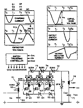
DC to D~ tep-D~n Tra~gor~tgo~
The TPCS~has the capability of step-up as well as
voltage step-down;~. :Figure~3:shows the~electrical
sGhematics;and some~elected voltage and current wayeform
2~0~ fo~a~three:~stage~:DC to ~C transformation. :In addition I
aveiselected~;a~negative to negative~polarity
transformation.~ Réversing all:of thè~shown~solid st~te
dèvlces~ould:~s~imply change the device: ~o a posi i~2 to
positive~step-down~voltage invert`er. : ~ ~
25~ The~ step-down~transformation cycle utilizes the
same~:three~:~subcy~les of charging, inversion, and:
:discharging~:of;~the;~TPCS capacitors. The major~ ~
dif~erences is that the internal TPCS process is executed
in the reversed order, as will become apparent from the
:0 following dis;cussions.~ Instead of charging the capacitor
: in parallel~and~:discharging them in~series, as is:the
case for the step-up, in the step-down the capac~tors are
ch~rged `in series~and d~ischarged~in parallel.
The charging is started with the triggering of ~he
:: :
- ,
. ~
~WO93/20610 213 ~ 9 7 ~ PCT/US93/03146
; ~;
- 15 -
input switch SCRo 61. With the utilization of the input
inductor Lin 62 the capacitor string, C1, C2~ C3, C4, C5,
and C6 will be charged to an electrical potential of
about twice that of the inp~t voltage Vin. Since the
: 5 charging occurred in series the capacitor polarity is
plus-minus-plus-minu~,:as is indicated above the
capacitors on the diagram. We recognize that this is the
; same elect~ic state as for the step-up configuration
; shortly before the TPCS discharge.
The second subcycle:is initiated by triggering the
switches SCRl, 66 SCR2~67 and SCR3 68 at the time Tl.
: With the proper selection of:the inductors Ll 70 L2, 71
and L3 7~ the inversion is completed at T2. During this
: cycle the voltage polarity of the odd capacitors are
15~ being changed~in the~same fashion~and with a time period
:control as has been flescribed for the step up
transformation above. The utilization of unidirectional
switches such:as SCRs;:~current is prevented from flowing
back.:~ The voltage~polarity of:the capacitor after the
2~0~ inversion cycle~is shown below the~capacitors. At this
point the:capacitor bank,~ measured from end to end, is
zero~as~:is~illu grated:with the:waveform in the upper
ri ~ ~hand~corner.~ We~recognize this to be the original
state of the~voltage~step-up:~configuration.
25~ With:the~inversion~completed the energy switch-out
cycle is initiated:by~triggering the switches SC~, 73
SCR5 and:~74~ SCR6~75~at the time~T2~ The diodes Dl~ 63
D2 6~:and D3 65~ complete the discharge circuit. The
: discharge period is~ again selected with the value of the
30: output inductor Lout 76~defining the discharge period to
the time interval of T2 to T3. The Free Wheeling diode
DFW :78 prevent the~recharging of:~the capacitor:bank,
a~lows:the complete~discharge of the TPCS capacitors, and
: aids in the~output filtering process.
~:: 35 As soon as;the~Free Wheeling diode comes in to
::: :
: '
WOg3/2061~ 213 2 ~ o ~ PCT/US93/03146 ,~
.
- 16 -
play the output SCRs will start to recover and the
recharge cycle can be started again. ~s can be seen this
type of step-down inverter is through-put limited and
allows both current and powe~ limitation. As soon as a
5 load fault is dete~t~d the output can be simply turned -
off by s~opping all triggeri~g outputs from the gate
controller. At this point the TPCS DC to DC step-down
inYerter will simply function as a DC shut~off switch.
: The voltage wa~eforms are shown in the upper left
lo hand corner and with it are also given the trigger timing
for all of:the SCRs:gates. The output switch and output
inductor currents are:also shown and assume that all of
~: the output SCRs are triggered simultaneously. ~f ~he
output load is low one~may reduce the output filtering
15 requirement by staggering the output by discharging two
capacitors at a time. By inserting two addîtional diodes
; in the circuit at positions labeled "A'l and "B" the
capacitors C5 and C6 can be discharged first by only
trigyering:SCR6 The~discharge of capacitors ~3 and C4 are
20 :next ~y triggering~S~R5. The final discharge o~
cap~citors Cl and:C2:is~:initiated with the triggering of
SCg4.~The~diodes a~:~position "A" and "Bt' prevent the
recharging of~the discharged capacitors.
~Qu~ar~t :8top-~p ~ ep-D~wn ~p~ratio~
25~ Xn the above description I:have shown DC to DC
convsrter for pos~itive to:positive:step-up and negative
t~:negative~step-down~. ;Inspection o~ both circuits shows
.that by changing a few components an output with an
opposite of that~of the input can be obtained. In fact a
30 single TPCS device can combine all possible or a selected
~::; : combined input and output polarity :options.
The schematics of Figure 4 shows a single stage
~:: TPCS that can step-up either a positi~e or negative
,
~ : polarity to either the same or opposite polarity. As
:: :
,.~W093/2~10 2 1 ~ 2 9 7 1 PCT/US93/03146
- 17 -
shown power flowing from left to right will functi~n as a
step-up inverter. With the input coming from the right a
step-down transformation takes place. The transformation
in both directions have, with all components shown, full
5 four quadrant operational options. One may implement-all
or only part of the options. The table in Figure 4 lists
the necessary components required for a specific option
with "X" designating the step-up and "Y" the step-down
components. The components required for a specific or
10 multiple choice operation must include all of the
~, ,
co~ponents under the designated columns. Of interest is
that the con~iguration~with polarity inversion allows
~; power flow in both directions without the increase of a
single additional component.
For example, the configuration for an A~ to DC
converter to~either step down or step-up can ~e derived
by the~combination of two parallel TPCS inverters. One
inverter would~be used~for the~positive to positive
conY~rsion during~the~positive~half of the input ~C cy~le
20~and~a~second invérter~for the negati~e half of cycle with
a~ne ~ ive~to~positive~transformation. Since the high
voltage switching section are the more costly components,
it is~prudent~to~maximize~ its utilization and combine in
one~device~both~functions~. ~For the above example of an
25~ AC~to DC~step-up~transformer/rectifier configuration both
functions~may~be~combined into one unit. This requires
the~sum of;~the~components~indicated by "X" under~olumn
;one~(+in to~+out)~ and;three; (-in to +out). For this
; example the high~voltage~SCR5 and the associated Free
30~;~Wheeling diode (not~shownj are shared for both halves of
the cycle.
In summary~the TPCS has a high degree of input and
output polarity~flexibility and all or a selected option
may be combined into one TPCS module.
i ~
wo ~3/2~l2 1 3 2 9 7 1 PCTIUS93/03146 ~
- 18 -
AC to AC Tr~nsformation
This æection gives an illustration of a single
phase AC to AC transformation device. It is configured
to use two parallel modules with each module operating in
5 an inverting mode. The device, as shown in Figure 5,
allows ~ontrolled power flow in both directions. From
left to right the AC is inverted and transformed up. The
p~wer flow can also be reversed with the flow from right
:~ to left. This will:result in a controlled voltage step-
lO down.
: Starting my description with the positive input
~: cycle and~with the power flow from the left. The turn-on
:: ;
of SCRl SCR~ and~SCR3 wil:l initiate the charging of the
upper capacitor string Cl to C6 through the diodes Dl, D2
15:and D3. The lower module is not active during the
posîtive input cycle and`its components are allowed to
cool-off.~ The:pos~itive:charging period is controlled by
the selection of~the~:Ll charging inductor value and will
yield~a capacitor voltage nearly twice that of the
20~ instantaneous input ~oltage, provided that the TPCS cycle
is::selected to be significantly shorter than an AC cycle.
Under this condition :the dévice operation is nearly
identical~ to~that~of~the above DC:transformation
configuration with~the~::exception of:~:a ~Islowly~ varying
;Z5~ ~ inpu t voltage.~
The~capacitor polarity is shown next to the
capacitors after~the~charging cycle is complete.'
Triggaring~SCR4 ~SCR:5~and:SCR6 wil1 start the inversion
cycle changing the~voltage polarity of capacitors Cl
: 3Q~:C3 and C5. This will produce a negative voltage of six
times that of a single~capacitor~across the upper
capacitor string.~ Triggering SCR7~will start the negative
voltage ou~put discharge cycle through the inductor L5
As soon as the voltage of~the capacitor string changes
3S from negative to positive polarity the SCR8 is being
. WO g3~20610 2 1 3 2 9 7 1 Pcr/usg3/o3l46
-- 19 --
triggered that will prevent part of the energy in the
inductor Ls to recharge the capacitor string ta the
opposite polarity. The SCR8 acts as the previously
described Free Wheeling diode, however a switched device
S is required for AC output operation. With the Ls inductor
current transferred to SC~8 the SCR~ will recover and the
next charging cycle, with a slightly changed input
voltage, can begin.; The L5 inductor in ~onjunction with
the output ~ilter will deliver a partly filtered AC
10 output.
The upper TPCS module operation, with the positive
input cycle and producing a negative output cycle, is
continued many times per cycle until the AC input voltage
swings negative. At this point the upper module becomes
15 inactive and the lower TPCS module is activated.
The operation of the lower module with the
negative input and~the positive output cycle is identical
with~the exception~of the inverted polarity. The TPCS
¢harging is~initiated;with the triggering of SCR1~
20~ S~Rll and~SCR12 charging the capacitors C7 through C12,
with the~polarity~as shown on the schematics. For the
i m ersion SCR13 S~Rl4~and SCR15 are used with the output
switching function~per~ormed by SCR16. The SCRl7 is the
positive~output~cycle Free~Wheeling switch. Two output
25 ;~inductors~are shown, one for each polarity. One inductor
co~ld~be~èliminated.
The~power throughput and output voltage regul~ion
is~per~ormed ~i~h~the~oontrolled turn-on of the above
switches~SCRs) using a controller and triggering module,
30 not shown to simplify~the schematics. The controller
would again sense the input and output condition for the
: .
- control function~and perform the regulation with the
; option as has been~described for the~abov~ DC
~ transformation. In addition internal TPCS diagnostic
- ~ 35 points are also monitored for fault protection.
:~
- :
2132~7i
WO93~2~10 PCT/US93J03146 ,~...
- 2~ -
Figure 5 sho~s for a complete AC cycle the TPCS
capacitor input voltage and the inverted outpu~ voltage.
: ~or constant TPCS frequency the output follows directly
the input waveform shape. Correction to input voltage
5 distortion can be made by altering within an AC cycle.the
:; TPCS frequency.
Th~ above single:phase TPCS AC to AC
,
transformation allows~regulated AC voltage
transformation:. With the appropriated control it can, in
:lO ;~additionr perform other functions such as turning the
power on and off,~perform~as a circuit breaker, perform
as~controller for a device start , and harmonic filter or
anti-harmonics qenerator.
~: ~ The confi~ ration:of Figure 5 allows also
15~regulated power flow~from:right to left. This direction
of p~wer flow will~yield a~voltage step-down with a step-
: down~ratio defined~by:`:the:;number of stages installed.Additional regulation~is obta:ined with~the inverter
frequency selection.~With:~the exception of the Free
20~ heelin~swit:~hes~, all~of the other components are used.
, ~ e~Freè~Wheeling:.:switch is the only~element that is only
,operational~at~the "transformer"~output end. In the
,.step-down mode~ the;upper TPCS~module~;:transforms~the
ne ~ tive~ inpu~voltage~from~the~right~to a positive and
25~reduced output~vo~ltage~:to~the~left,~while the lower
mo~u~le~:generates~the negative output cycle on the left
with;~a~:positive~input:~Prom the right.: In this~mode of
operation the~capacitor~strings~are~-~oharged in series
with~a high volta,ge,:with capacitor terminals connected
30:~:wit~h alternating:polarity. The inversion cycle changes
thé:polarity of~half:~of the capacitor:to the
configuration as shown on the schemat~ics. This allows
the~energy to be extracted to the left. The additional
SCRg and SCRl9 not:utilized in the:step-up
; 35 transformation, perform the Free:~Wheeling switch function
::: : : : :
~: ~
,~WO93/20610 2 1 3 ~ ~ 7 1 PCT/US93/03146
- 21 -
for the positive and negative cycle respectively. The
filtering sections on both the input ends, not shown,
assure a smooth input and output power line.
The above single phase AC to AC TPCS
5 transformation module can be used as a building bloc~ for
a bi-directional polyphase regulated voltage
: transformation system with an effective 180 degree shift
: in phase angle.
AC to DC Tran~forma~ion/Inver~ion
State-of-the-art generation of high voltage DC
from~ an AC input:requires an AC transformation followed
: by a rectificati~n:step~ Power distribution syst~ms
typically use an AC transformer at grid frequency to
; perform:the:voltage step-up and a rectification step at
lS high Yoltage. mis~: is:~an efficient process, however
harmonic filters are~required to eliminate harmonics
:generate~ by the rectification process. In addition
power: factor corrections:~::are:required. DC power levels
in éxcess~ of one;~megavolt;are generated this way for long
: 2~0 ~distance:power transmission.:
For~:~lower~weight~:and compacted:ap~lication the
S~h~w~arz conver~er~may be used by first re~tifying the AC,
conver~ing~the DC~to~high~frequency AC, performing the AC
transformation with~a~significantly~:reduced transformer,
;25~ and~finally~ rectifying:the~ high frequency stepped-up AC
power~to~producè:DC.~ The transformation process at high
: frequency significantly reduces the~transformer weight,
however, at the expense of reduced efficiency. In
addition this process~further pPnalizes the efficiency
,
~ :30: further:as the ou~put voltage is increased much over a 50
-;:~ : KV~output~
In contrast my:TPCS approach uses the AC input
directly and requires~no transformer at all. In addition
no harmonics are generated with the~TPCS conversion
-;~ :
329~ ~
WOs3/2061~ ~ PCT/~93/03146 ~
`
- 22 -
process and the AC input power-factor is-for all
practical purposes unity. By eliminating the transformer
and harmonic filters the TPCS AC to DC conversion not
only can compete with the commercial efficiency at the
5 same voltage and power level, but also is more e~-onomic
and much smaller in size.
The DC output can~be obtained using either two
TPCS modules as described above. One module would
transform the positive and the second one the negative AC
lO input cycle to high voltage DC. A second option is shown
in Figure 6 that combines both functions in one module.
It~performs the~positive to positive and negative to
~` positive functions~and has~the sum of the components
listed in the first and third columns of the table in
15 Figure 4. Combining the~low voltage input functions and
sharing the high~voltaage output functions makes in many
applications technical and economical sense since it
;ahares~the two high voltage output switching section
c ~ onent~s of~SC~g~and~Free Wheeling Diode D
20~ For the p~s~itive~AC cycle SCR1 SCR2, SCR3 .~CR4j
S~R5~and SCR6 are~turn~d on to initiate the TPCS charging
aycle;.~ miS~ charges~the~capacitors with the polarity as
shown below;the~capacitors~. For the~positi~e input cycle
triggering SCR7~ SCR8,~and SCRg~starts the inversion.
2 ~ This~will result~in~a~capacitor po1arity as is shown on
to]~ of~each~capacitor.~ The inversion~will yield an
output~voltage~of~;2nVin,~ where the "2"~comes from the
resonant charging~process ~nd "n"~are the ~umber of
capacitors in~the~capacitor string. Triggering the SCR19
30 will initiate the~output cycle through the~output
inductor ~5 The~càpacitors Cln and Cout are~part of the
nput and output~filtering section respectively. ~he
Free Wheeling Diode DfW prevents the capacitor bank
` voltage from swinging negative and allows efficient
35 output energy transfer.~ The positive TPCS operation is
`
~wo g3,206l0 2 1 3 2 ~ 7 1 PCT/U~93J03146
- 23 -
repeated as long as the input cycle is positive.
As the AC input voltage swings negative the
controller and triggering module (not shown) switches
; over to the SCRlol SCRll, ScRl2,-scRl3~ SCRl4, and SCR15 for
5 the charging cycle leaving the capacitors with the
polarity as shQwn in the circles. To produce a positive
~: output vol~age the SCR16 SCR17, and SCRl~ are used to
invert the other set of capacitors. The discha~ge cycle
is identical to that of the positive input cycle
10 operat:ion and again uses SCR19 and Free Wheeling diode
w. ~ : :
: The input and~output current is as shown (not to
~ .
scale:) in~Figure;~:6::and consists for an AC input cycle of
~: many TPCS cycles. Using a high frequency output filter
15 will produce~a~stepped~up~voltage with a shape that is
;nearly identical::to that~of a full wave rectifier. To
reduce~the:input~line~ripple for a TPCS~single phase AC
to~DC~transf~ormerjrectifier~standard:filtering has to be
:added to the:output.:~ As with:a regular filtered full
20~wave~;rectifying configuration phase distortion takes
pla¢e::with harmonics~generation, since during the low
voltage part of the input the~rectified voltage is lower
than~the~filtered:~output voltage~and no energy can be
nsferrèd.~ This~:~applies also for~the TPCS
25~ r~ctifi¢ati~on process~but~to:a lesser degree, since the
TP~S~transformation~;~ratio can be selected to be
;irbitràrily~high~without::major impact on the system
ePfic~iency.~ ~Such~harmonics can~be completely;eliminated
with~the single as~well as with a multiple phase TPCS AC
30 to;DC inverter. :~
One approach~to eliminate input harmonics is to
ad~to ~he Figure:6 circuit:inductor L~ ,SCR21 and SCR
The functio~ of~these~;components is to invert the
capacitor bank if the bank voltage is too low. By
:;: 35 invertlng the complete capacitor~bank the capacitors will
: ~ :
213~97~
W093/2~610 PCT/~S93/03~46
- 24 -
start out with a nonzero voltage of opposite polarity
than the input voltage. This condition will allow the
capacitor bank to be charged repeatedly until the voltage
is sufficiently high to allo~ a full discharge into the
5 DC output grid. The charging process is performed in..
such a rate to extract the correct energy and charge from
the ~C input cycle to prevent harmonics generation. The
process for the positive input cycle is as follows. If
: ~ ~ after the charging the capacitor voltage is too low, the
10 following switches are being triggered; SCR20 SCRll,
SCRl2 SCR13 SCRl4 and~SCRls The current will be flowing
through the inductor L6 until the capacitor changed their
respe~tive:polarity.~ The inductor value can be selected
to optimize this operation. After the bank inve~sion is
~5 complete a new:posi~ive input charging cycle is initiated
aæ~described:above~. Since an initial voltage of negative
: polarity is on:the capacitors,:the bank will be charged
to a higher voltage.~ This process ~an be repeated
several times~until~:the voltage is sufficiently high.
20~:~For~the negative cycle the~same procedure can:be used by
se1ecting~the~correct~switches. The Table in the figure
ists:all of:the swi~ches used for the various
operations~ ;The~described bank inversion procPss fall~
under "IN~UT:INVERSION":column.
j , ,
:
- -
:
:: :
: :
,~WO93/2~10 2 1 ~ 2 9 7 1 PCT/US93/03146
.~
- 25 -
To calculat~ quantitatively the multiple charging
process let us assume that the input voltage is Vi and
the initial capacitor voltage i5 given by Vci. The final
capacitor voltage will be; -
VCf - ~ Vi ~ Vci
: this equation applies as long as the initial capacitor
voltage is less than the input voltage. This yields a
charging voltage of Vcl = 2 Vi for the first charge cycle,
:~ ~ince the initial capacitor voltage is zero. After the
~ 0 first charge cycle the energy in the capacitors is;
; : El = 12 C~Vi2
where C is the apacitance of an individual capacitor.
By inver~ing all of ~he capacitors the initial Vci.fo~ the
: second charge cycle is -2 Vi and will yield a charge
15 voltage of~Vc2:= 4 Vi;and nergy of E2 ~ 4 El This can be
repeated to~yield after~ " cycles a capacitor voltage of
V~n:-~2 n~Yi and energy of En o n2 El.: The use of this
cycle~inversion in conju~ction with the~appropriated
inter~als between charging cycle allows the loading of
2~0~the~AC~i~put~such~that;no harmonics are~generated and the
effe~tive~:load~f~or the~AC~:grid appears to be resistive.
A modified~cha~ge approach can be used wi:th a
polyphase~A~grid:that does~:not~requ~ire~the~fu~l bank
inversion~between charge cyc~e. By charging sequentially
25~ from~di~ferent p~hases~with opposite~polarity the~bank
inver8ion:and~some~switches can ~e~eliminated~with an
incréase~ of ~the~ lo~ic complexity. :This will be fur~her
cov~red in~a later~ection. ~ :
, ~
Polypha~e A~ to D~ ~ra~formatio~/I~ver~io~
30~ The~:single phase AC to:DC~conversion~Gonfiguration
described in the previous~section can ~e used~as~a
building block. However~ost high~power converters use a
pol ~ ase input such as the output of a generating plant.
The:single phase~TPCS step-up transformer/rectifier
, :
:
~i~2~
W093/2 PCT/US93/03146 ,~
- 26 -
module input section described, can be modified to allow
inputs from more than one phase. This modification in
conduction with the appropriate switch control and
trigger logic can obtain ha~monic free input and output
5 power wlthout the use of harmonic filters.
A balanced polyphase generating system delivers
constant power if operated into a linear resistive load.
To simulaté such a resistive load the TPCS must extract
from a single phase~a~power~level that is proportional to
10 the square of the instantaneous line voltage. For the
; simple charge mode~described for the AC to DC
transformation process the inverted TPCS can not inject
the energy into thè load during the low voltage part of
the AC cycle. A repeated charge and inversion process
15 with one phase may~be~used~to solve this problem. This
section will describe~a second method that utilizes the
voltage input from~a plurality of phase. This
architecture and~mode~of~operation can be also adopted
for~reactive~power génerators,~harmonic fil~ers and can
0~Gorrect the power in an~unbalanced line.
Figure 7 shows~the schematic diagram of a three
phace~AC to DC con~erter. The converter module ~ontains
the~components~as~shown~in~Figure 6 with two additional
input~sections~connected to~the electrical point "A" as
25~ 1abeled~in Figure 6.~ With the additional two input
sections~the device can~accept the~ input from all three
grid~phases~and for~both~the;positive and negative AC
cycle. ~he output~will be a constant and stepped-up
voltage DC with constant p~wer. The other important
; 30 ;feature is that controlled energy can be extracted fr~m
all three~phases~at any voltage specifically at the low
voltage part of the~cycle thereby eliminating the
ormation of harmonics~on the AC input lines and ripple
on DC line.
,~ :
-~ 35 The charging cycle of phase 1 is controlled by
:~ :
:~ :
.~WOg3J20~10 2 1 ~ ~ ~ 7 1 PCT/US93/03146
- 27 -
SCRl and SC~lO and is assumed to have the voltage
waveform of Vl(t) =A cos(w t). Phases 2 and 3 are
ntr~lled by SCR20, SCR2l, an~ SCR22 SCR23 respectively.
The waveforms are plotted in Figure 7. Specifying a
5 regu~ated and filtered output of DC of VDC =3*A the -
inverted output voltage must be a minimum of 6*A and
therefore, requires that~the capacitors are charged to a
vo~tage of a minimum of A. Using the resonant charging
mode it: follows that the minimum line voltage must have
lO an absolute value of A/:2. The harmonics are generated on
; phase 3 by not extracting energy for an electriaal phase
angle between 0-60~and~180-240 degrees. This problem can
: be simply reatif~ied~with~a consecutive bipolar charging
sequenae as will be described for the first 30 degrees
15~ ;with the aid of~the voltage waveforms in figure 7.
During the first 30 degre~e:electrical phase angle period
phase 2 can charge~the capacitors to the required ~oltage
;A~and~a~single charge operation~is;used. The problem is
that phase 3 has:~an::absolute:line voltage of less than
20~A/~a~ By triggering~SCR23 the capacitors will be charged
negative~:to~a:;value~2 V3 .and will extract an energy of E3
2 V32 ~ ass~ing~unit~capacitance for simplicity). With
;the~capacit~r bank being negative~we next trigg r the
S ~Por:~a~positive~charge~cycle of~phase l. This will
5~;charge~the~capacitor~bank~:to V31 = 2: (~Vl - V3~. Since V3
is~negative,~the::~chargé.voltage is larger then "A". At
;this`~point~the~TPCS performs an inversion followed by.an
extraction aycle.:~
The~total;energy:extracted transferred is ~t = 2
30 ~(Vl - V3)2. The:energy extracted from phase l is E3l ~ = 2
V~ Vl - 2 V3) :The~two~step charging process increases
the:energy extraction.~ ~
The two step charging process can be reversed by
first charging with~phase l followed by phase ~. It can
35 be shown that the total energy transfer is the same,
:
:~: -
W093/2~10 2 13 2 ~ ~ ~ PCT/US93/03146 .~
- 28 -
however the energy extracted out of phase l is El3 l = 2
Vl2 and from phase 3 El3 3 = 2 V3 (V3 - 2 Vl).
The graph in the upper right hand corner of Figure
7 shows the energy transfer over the first 30 de~ree
5 range. The upper graph shows the total energy transfer
from both phases. The two remaining curves show the
energy extracted from phase 3 using for the lower curv~
the charging sequence of phase 3 followed by pha~e l,
while the center ~race is $or charging sequence of phase
lO l first followed by phas 3. The energy extracted from
phase l is the difference between ~he total energy and
; ~ the energy given with the curves shown for phase 3. The
energy extraction result from a given phase is
drastically different depénding on the order of charging
15 and can be fully utilized in the optimum control of the
TPCS transformation:process.
At the 30 degree point phase 3 becomes positive
and the two step charging scheme is being used between
phase~:3 and the negative phase 2. This process continues
:20 ùntil phase 3 reaches a:~value of A/2 at th~ electrical S0
degree point. ~At thi~s point the rolls between phase 3
~:~ and l are:exchanged and:the process continues.
The controller monitors the input and output
:~oltage and controls the switch triggering sequence and
25~ the time;periods ~etween charging. Sev~ral TPCS modules
may be used to increa~se the power throughput and re~uce
:~ the high frequency filtering requirements. Some of the
inductors, input :and;output filters may be hared.
In summary the:TPCS polyphase AC to DC converter
30 can be configured to allow constant power throughput thus
: :eliminating ~ll harmonic filterinq requirements on the AC
: as well as major ripple filtering on the DC side. In
addition a:unity power factor is maintained, since the
current and voltage is maintained to be in phase.
-.WO93/2~10 2 13 2 9 71 PCT~US93/03146
;.:;
- 29 -
DC to AC Co~ver~ion
The reconversion from high voltage DC to a
polyphase AC can be performed at the end of a long
distance DC ~ransmission li~e or at the end of a DC power
5 ~istribution system . The DC power can be converted to a
balanced three (or multiple) phass AC outpu~ with
constant loading of the DC input. The output can be
precisely matched~to the~phase,~frequency, and voltage of
i~ ,
the existing grid or to a specific output requirement.
; 10 In the TPCS conversion process the DC line will be loaded
again uniformly and the converter will provide a harmonic
f~ree~vo~tage or power regulated AC output. The DC power
is stepped down to~the required AC voltage level without
the requirement of costly~transformers, harmonic filters
;15~ on the AC end and input filters on the DC side.
The TPCS inverter~is a power converter in which
the~normal direction of power flow is from a high voltage
DC~source~to an AC~load.~ Its typical operation control
modes~can be~classified~as~a Variable output Frequency
20~ ~adulated ~VFM)~inverter. ~he TPC~S and its control
ystem~can re~construct~an~unlimited family of output
;waveforms. one of the~waveforms can be the desired AC
output wLth the~des~irèd~voltage, frequency and phase.
;For~an~;AC~waveform recon~truction the TPCS system
25~ can~be~fully oharged~from~the~DC l~ine~but with
oontinuously~varyin~ charging in~ervals during the AC
output~cycle. The interval spacing~will be inveræely
proportional~to the~;square of the instan~aneous output
voltage requirement.~As~the~AC power requirement changes
30 ~the~charging intervals change invers~ely with the power
demand. ~he TPCS inverter~could also be operated as a
; constant frequen~y~but;with Variable~Amplitude (~AC).
This~requires a variable~output amplitude control with
the energy output pe~r pulse being propor~ional to the
35 s~uare of the instantaneous output~voltage requirements.
,
W093/2~10 PCT/US93/03146 ,~
- . . .
- 30 -
Each approach has its ad~antages and disadvantages. The
mode of operation, described below, uses a combined mode
and is of Variable Frequency with Variable Amplitude
: Control ~VFMlVAC)~
: 5 ~ Figure 8 shows~a module to reconstruct one phase
of a polyphase AC line from a DC input. The control :~
circuit has been neglected~for clarity. A high DC filter
~ allows the series charging of the capacitor bank
',~;;~ ,:~ consisting of a three stage TPCS module. The capacitor
10 bank is resonantly charging through the inductor Ll by
triggering SCR~ For~the reconstruction~of a positive
.output cycle the inversion switches SCR2, SCR3 and SCR4
are used. The~capacitors:voltage polarity before and
after the positive~cycle inversion are shown by the upper
lS,:and~lower~set~of~signs respectively. The':;middle set of
:: signs next to the capacitors~shows the inverted
capacitors voltage~polarity for the negative AC cycle.
The'positive output~cycle discharge is initiated by
triggering SCR~, SCRg, ~SCR10~and~SCRl~, SCRl2, SCRl3. As
20~ before~:the 5CR20 i~æ~used~as a~Pree Wheeling Switch ~o
'prevent~ the~:recharging~of the capacitor bank:. This
allows~the~maximum~power:~throughput at the top of the
cyole,by~dischargi~ng:~all;of the~capacitor~s
simultaneously:.~ During~the lower part of~the,AC cycle
25~the~capacitors~can~be::;discharged at a sIower rate ~y
,using,~a~sequential:~discharge.~ The electrical circuit
shown~all~ws~ such~a~mode~by~f~irst ~riggering~SCRl0 and
SCRl3~:to~discharge~C~ and~C2. Triggering~S~Rg~and SCRl2
ext,:while SCRl0;and SCRl3.are still conducting, will
30 allow the~discharge~of~;~capacitors C3 and~:C4~ :The diode D3
is~added~to:prevent~the~capa:citors Cl~:and~C2 to be~
recharged-.~ Finally~the:set of C5~and:~C6:~Cl are
discharged,~ with Dl~being used~as~a blocking~diode to
prevent the:recharging ~of C3 ~and C4. This mode of
35 charging:and discharging allows~a smoother output for the
: .-
~: .
_WO93/2~10 213 ~ 9 71 PCT/US93~03146
.,~j
~, ,r
lower voltage part of the AC cycle and with it a reduced
high frequency filtering requirement. The disadvantage
is ~he additional cost of the diodes and itis associated
voltage drop and power losses.
The negative cycle is reconstructed in a simi-lar
manner. The TPCS charging cycle is identical. The
difference starts with the negative inversion ~ycle by
triggering SCR5, SCR6 and SCR7 For the negative output
cycle the switches SCRl4, SCRl5~ SCRl6,SCRl7, SCRl8~
10 DCR19 are used. The~ diodes D2 and D4 allow a slower
output discharge. In the upper part of Figure 8 the
charging and discharging current sequence are shown
schématically. Only a limited number of cycles are shown
for clarity.
l5~ To reconstruct a~full~polyphase output several of
such modules are required~with each one being
appropriately controlled.~ balanced harmonics are
generated by the-load the~TPCS~master controller can
contE~l the output to neutralize these harmonics. The
2~0~ o ~ ut becomes~simply the~superposition of several
fr~equencies~with~each frequency being~controlled in
amplitude~and~phase.
V~ri~ble~Freque~cy~Co~Verter~
We have~seen~that~the TPC5 can extract ~onstant
2~5~power~from~a~polyphas~e AC grid or a DC lîne. This power
can~be~used~to~reconstruct an AC~polyphase AC grid with
regulated~output~;~as has~been covered~above. The~
xe¢onstruction o~the~AC grid is not restricted to the
input;frequency. ~ miS ~ allows the use of the TPCS AC to
30 AC transformation system~as a direct link between two
independent grids,~operating with~a~different ~requency
or a~different pha~se~
Furthermore the AC to AC TPCS system can be
controlled to produce a~variable frequency output for the
3~ regulation of high power linear induction motors. Since
',
:
WO 93/206~32~ PCI`/U~g3/03146 ,~
- 32 -
each output phases of the TPCS can be controlled
separately the functions of two phases can be switched on
a subcycle time basis producing a change in the phase
sequence for an instantaneous change in the rotation of
5 induction motors.
The use of a TPCS AC to AC step up converter could
be used between a gener~ator and the power grid. This
would significantly improve the power grid
~electromechanical stability cince the rotation of the
lO generators are not~required to be in perfect synchronism
with the grid. In fact most gear boxes of generators can
be eliminated, since the TPCS AC to AC converter can as
efficiently convert~and transform the balanced grid
generator output of any frequency to match the frequency
15 of the power grid.
In summary the~TPCS AC to AC converter can be
controlled to produce a Yariable frequency with
simultaneous amplitude~control with an efficiency similar
; to that of a standard AC transformer. No upper frequency
20~ output~restriction~does exist such as for the cyclone
~onverter.~ ~In addition no harmonic or phase distortions
are~introduced on to the input gFid.
R- ~ late~ V~R Gen~rator~
TPCS~modules can~be configured as a fast response
25 ~phase~angle~correction~system for~ both leading and
la~ging ~AR. As~described~in~the~AC~to DC power
transformation a TPCS module can extract power or charges
from a low voltage line and injects it into another line
having either polarity and also higher instantaneous
30~ voltage. With the fast TPCS operating characteristics
such a VAR generator can respond on the time scale of a
fraction of an AC~cycle.~
f properly controlled the phase angle correction is
:~
~ performed without generating either harmonics or phase
~: :
: ~ : ' .:
~qWO93120610 213 2 ~ 71 PCT/USg3/03146
. . .
distortion. For balance polyphase grids my ~AR generator
configuration does not require the storage of energy for
part of a cycle as is normally required for most
operating systems. Howe~er, for sinsle phase VAR
5 correction existing capacitor banks may be used in
conjunction with TPCS modules to control tha desired flow
~of reactive energy. ~y either extracting from the line
or injecting back into the line the correct charge over
the complete cycle, harmonics ganeration can be
~10 completely eliminated. This is performed, as for all of
the described TPCS operation, without forced commutation
of the switching elements. The natural or self
commutating configuration of the TPCS modules add
significantly to the overall system reliability, reduced
15 co]~plexity, and eguipment;cost.
For a polyphase~grid the TPCS VA~ control can be
perfor~ed with independent singla phase VAR controllers.
Reduction of the~ene~gy~storage requirement can be ~
accomplished if;the ~en~ergy~storage capacitor banks are
20 ~shared between the TPCS~single~phase VAR generators.
Since~for a~balanced grid the sum of~the~inflow and
outflow~of reactive energy and~reactive~current into the
energy ~storage bank is zero at all instances o~ the AC
cycle~it~becomes obvious that such a shared bank can be
25~-s~ignificantly;re~uced.~In~fact the capacitor bank and
its~aharging~and~discharging steps~oan~ be completely
e~liminàted with the reactive current extracted from one
line and with the~direct reinjected into another line.
The simplified schématic in Figure 9 illustrates such as
30 system.
The illustration shows a controlled TPCS ~AR
generator for a~three phase grid with a neutral. This
architecture is equally applicable for grids having
larger numbers of phases. Furthèrmore, it is not
35 necessary to have a neutral since TPCS VAR generator
2 1 ~ ~ ~ 7 1
W093/2~10 PCT/US93/03146
- 34 -
modules can be directly connected between phases.
Figure ~ s~ows a TPCS module with both the low
voltage and high voltage sections connected to all three
phases of the power grid. This system archit~cture is a
5 generîc module and can operate as a regulated ~R
generator and harmonics f il*er . Both ends can be used
or charge extraction~or injection. For VAR generation
:~ mainly the low voltage end of the TPCS will be used. For
harmonics filtering functions the front end is mainly
: ~ 10 u~ed for energy extraction from the grid and the high
voltage end for the energy reinjection.
The VAR generator controller can either regulate
the reactive curren* or reaCtive power flow. Controlling
either one will control automatically the other
15 parameter. This~will~become apparent from the exampIe
and can be readily~proven ~athematically.
Assuming~that a VAR generator is connected as
shown~in Figure~9 t~ a~three phase grid with a reactive
load.~ The voltage~;and reactive currents~are given by the
20~following equations.~
Vl=Vm~cos(w*t) ~ Irl=Iro co~(w*t - ~/2)
V2=Vm cos~(w*t +~2~/-33~ Ir2=Iro cos(w*t + ~16)
V3-Vm cos~(W*t~;+~4~/3)~` Ir3=Iro~cos(w*t + 5~/6~
Figure~10 sh ws~thc power voltage,~reactive current, and
:25: rea~-tive~:~ps:wer flow of; :all three phases. The operation
will be~demonstrated for a phase angle ~of w*t = ~ll2 or
15 degrees. ~ ~ ~
.
From the traces it can be seen that energy needs
;to~be extràcted;~from~he grid when the shown reactive
30 power is negative.~We~start out by triggering S~R4 to
charge the capacitor from~phase 2 through the inductor
L2.~ The charging per~iod;is again controlled by the value
of the inductor.~Table I shows the result of the
~: :
::
^ WO93/20610 2 1 3 2 9 7 1 PCT/U~93/03146
~ 35 -
operation. Column 1 d signates the operation and lists
the phase involved, column 2 lists the control switches,
column 3 is the initial TPCS capacitor bank voltage
normalized to the maximum phase voltage amplitude Vm,
5 column 4 gives the final capacitor vol~age, column ~ -
lists the normalized charged transfer to the phase, and
finally col~mn 6 is the energy transferred to the phase
normalized to the energy for the bank charged to a
: ~: vol~age Vm~
From the first operation we see that energy was
~ extracted from phase 2 and that the bank was charged to
;~ twice the volkage of ~he phase. The positive number of
the charge transfer column indicates that a positive
current is being induced. The final voltage of the first
l~ operatio~ becomes the initial capacitor voltage of ~h~
: seco~d c~ ation. The second operation is initiated by
triageri,~g SCR5 in oder to inject a negati~e charge and
energy into phace 3.~: The final capacitor voltage and
charge trans~er is~given by;:
20 V~ = 2 Vph - Vin~ Q = C ( Vin - Vf
: The energy injected~ints phase 3 is:
=~;C ( Vin2 -~`~f2~:)/2
and is positive as~expertedO Operation 3 is an other
recharged:cycle;from:phase 3. We note an increase in
: 25 ~ener~y transf~r from;that of the first operation as a
result of the initial capaci~tor voltage.
Operation~4~i a~second~charge~:transfer to phase
3~:~ This will~leave the~bank at a final:positive v~ltage
~of significant amplitude to inject charge and energy into
30 phase l. This will leave the capacitor bank ready for
: another~recharge from phase 2.
: The~above sequence of ~ycles extracts energy from
phase 2 and transfers it to both phase l and 3. Table II
: shows th result of~the 5 operations described. Column
35 ~ shows the total charge transfers and can be
~:
W093J20610 213 ~ PCT/US93/03146
- 36 -
quantit~ti~ely compared with the theoretical requirements
by multiplying the reactive current by the appropriate
; time interval. The time interval was selected to match
the charge injection requirement of phase 2. The
5 operation is selected to balance correctly the char~e
injection be~ween phase 1 and 3. Column 3 shows the
reactive energy extraction or injection of the three
; ~ phases and can be compared to the theoretical value in
column 5. No attempt is made to track the energy
10 transfer since by transferring the current directly the
energy comes out automatically. Table 2 shows also the
~: net charge and energy transfer for all three phases which
should be zero. The computation balances for the
~: exception of the residual energy in the bank. This
1$ :energy~will~be used in:the following operation~
:The operation to this~point involved simple charge
and discharge operation. Table 1,~operation 6, 7, and 8,
shows~an: important~sequence of oper:ation when the TPCS
capacitor bank vo~ltage has the wrong voltage polarity for
20~:charge~in3ection into~pha~se 1. This requires either a
complete voltage:~reversal internally:of the TPC5 or can
be~performed~externally with the addition of the
inversion:section:~consisting of:L7:and witches SCR13 and
5CR14. ~After~the~number ~ recharge cycle the capacitor
2:5~bank:is~1eft~:with a~negative ~oltage. By triggering
: 5~R14 thé~ bank~polarity was inverted before the~charge
injection ~operation~in~olving phase~l could be performed.
:The control operation appears at first
complicated, however the logic can be relatively easily
30~formulated and can be~read:ily implemented using modern
: control technology. A controller~:would:detect the
:reactive:current and compare it with the preprogrammed
requirement. The~ frequency of operation would be
selected to meet the magnitude of the VAR generating
35 requirement. Computations would keep tra~k of the
:: :
~: :
~WO 93/2~0 2 1 3 ~ ~ 7 1 PCT/US93/03146
... .
; .
- 37 -
reactive current flow distribution on the three phases
and select from a series of operational seguences the
best one to meet the required reactive current
distribution and stay within T~CS operational
5 limitations. -,
The described ~AR regulation can be modified to
operate between phases if a neutral is not available.
This ope~ation requires additional sets of switches on
the lower terminal of the Nodule. In addition the
10 complexity and component count is increased, however some
system~advantages may be~realized. Finally, it is
understood that several of such modules may be operated
in~parallel with some modules specifically designed for
, ~dedicated operation~and operating between dedicated
15 phases.
The operation described in this ~JAR generator
section~ did only use the TPCS front end as a;capacitor.
In fact~for~simple~V ~ ~correction the TPCS voltage step-
up~operation is~;not re~uired and a simple capacitor can
2~0 be~used in its place.~This front end de of operation
can~be~ used not only for the VAR generation but can be
xtènded~to~the~ other~operation described in this
specificat~ion. ~Without the TPCS step-up~or~step-down use
can~still synthesize single or polyphase ~C output, DC
Z5~ output ~or output~of~other waveforms.~The~input~may be
,from an~AC grid o~from a DC source. ~The limitation is
in the output voltage range only. Without the TPCS an
ou ~ut of the same~or'~redùced voltage level is most
:: : : : : :: :
practical. ~
30 Induotive Energy 8torage
The ba~ic TPCS allows~a complete electrical
,disconnection between~the input and the output. This
reliable high voltage "Opening Switch'l function îs the
; missing ingredient for practical inductive energy
:~:: : : : ::: :
:: : : ` : : : :
:~:: :
. WO93/20610 PCT~US93/03146 ~
., .
- 38 -
storage.
As many ~tudies have shown, inductive energy
storage requires much less weight, volume, and is
significantly lower in capital cost.' The implementation
5 of the TPCS as an opening or disconnect switch allows..the
practical implementation of such an inductive energy
: storage system.
:~ Figure 11 is a:simplified schematic for a TPCS
magnetic energy storage~'assembly 60 that allows the
10:~ controlled build-up of a large current and inductive
energy in an inductor 61 from a power source. With two
or more~TPCS modu~les the charging can be~effectively
continuous. In~addition~a free wheeling switch (SCRfW) 62
~:: can be used to circulate the'current during the short
15 TPCS recharge period. The~free wheeling SC~ is turned
off every~time the TPCS module~is injecting energy into
the inductor.~
With enexgy buil~d'up~to the desired value~the TPCS
harging~:system is~:stopped and the:output switch (SCRoU~)
20~63;is~turned on:to,extract;the~magnetically stored ,
energy.~ At:this~point~the TPCS,:~connected throu~h the
,SCR~n~64.~to~thé~inductor represents:a small and discharged
aapàcitor:~bank.~In~addition~this bank will become
etely~isolated~from the~inductor as soon as the SCRin
:2.5:~ is~reverse biased.~ If~the output interface circuit is
,properl:y~:des~ign2d,~ the~0utput can be~ g opped with:a new
charge.~injection~from~;the TPCS charging~module into the~
inductor~as::~long~:~as the TPCS~instantaneously in~ected
current: is;larger;than~the output current. This will
30~back-bias the output~SCROut assembly~and turn it o~f. At
:this:point the;:new inductor charging~cycle is started. A
filtering network~65~may be added for component
protection.:~
The system is~controlled by gate trigger
; 35 controller. It receives the external operational
:: :
~,
,
: ~ :
~093~20610 ~1 3 2 ~ 7 1 PCT/US93/~3146
"~
- 39 -
requirements, in and output conditions, and generates the
æwitch trigger signals.
Reli~bility I~p~t o~ the TPCS
A solid state stack ~ailure in a standard inverter
5 or converter will either cause a direct AC phase to-phase
or direct DC line~short. A similar component failure in
a TPCS inverter or converter will not cause the same
atastrophic failures and requires much less protection
and fault clearing~equipment. In the basic TPCS
lO operation either a~relative small capacitor is being
~; charge~ from a line or;dischargéd into a line. A short
of a solid state~stack will~not cause a major inrush
' current and can be cleared much more readily. With
several TPCS modules operating in parallel the defective
15 module can be isolate~and the remaining units can remain
operatio~al with only a reduction of the maximum power
throughput. Repairs can then be scheduled for the
appropriated time.~
The operation of the basic TPCS are in three basio
20~,steps, i.e. charging the~capacitors, inverting the TPCS
capacitor chain`, and discharging the inverted chain. A
p~is typically completed bèfore;the next is being
initiate;d.~;If~a~;~failure~is detected~and the sequence is
rupted no;short~current will flow~from the input to
25~ the~output.~ At~that point the system~can be isolated
without~the~use~of high power air bla~st switchgear. This
is~especially~bene~icial on the DC~side, since DC faults
are~much~more difficult~to clear.; In fact TPCS AC to AC
transformation unit,~AC~to,DC converter, and DC to AC
30~inverter~can be each~used as an effective high power and
high~voltage interrupter. In addition the basic operation
of any described TP~S de~ice has a maximum power
throughput and can not be overIoaded.~ The TPCS can be
used as an e~fective power or curre'nt limiting de~ice.
35 ~ Although the invention is described with respect
:. :
:
,
:: :
2 ~ ~ 1
WC~ 93J20610 PCr/US~3/0314~ ~
-- ~0 --
to a prefer~ed embodiment, modifications thereto will be
apparen~ to those skilled in the art. There~ore, the
scope of the invention is to be determined by ref erence
to the claims whis::h follow.
I Claim as my inventic~n: . -
.
:: :
::: : ::
:
;
,
,~
: :
: : :
: ~ i