Note: Descriptions are shown in the official language in which they were submitted.
93/~t~581
~. 3 ~ 9 ~ b ~c'~/~s9~/o~sa~
1
SEMICONDUCTOR OPTICAL, DEVICES AND TECIiNI~UES
FIELD OF THE INVENTION
This invention relates to semiconductor devices and, more
particularly; to techniques which employ a grown native oxide
of aluma.num to obtain improvements in III-V semiconductor
lasers dnd wa~rec~uides~ and alto relates to semiconductor
lasers wh~:ch exhibit imprQVed properties, including improved
single mode operation, optical switching and bistability.
The p~°es~nt invention was made, in part, with U.S.
Government support, and the U.S. Government has certain fights
in this invention.
gp,CKGROUND OF THE INVENTION
Semiconductor lasers in the shape of a ring, or a partial
virago have been known in the art-for a number of years.
Reference can be made, for example, to J. Caxran et al., IEEE
~. quantum E~eC~r~~. ~E-~ ~ (..~~~0.).% A.S aH. ~~a~~et. al . ,
APpl'. P~~s. I,.ett. 36; 801 (1980) and PSansonetti ~t al.,
~.lec~tron Lett. ~3, 485 (,1988) . These tlrpes of devices have
carious applications and proposed ~~pla.cations. For example,
3t hays been proposed that a semiconductor.ria~g lassr; in which
light circulates in both clockwise and qe~unt~r-dlockwise
diredtioins,,could be used asa very small and inexpensive
,, gyx~eascop~. Briefly, certain'motion of the gyroscope would
have a different effect 'on the clockwise' and counter-Gloc~c~aise
fight components, and the effect can be deferred -~o determine
'the motion or orientation of the de~rice.' R~.ng lasers,, or
;'circular resonators" hsve also been proposed far applications
such as filtering and multiple~cing in so-ca~.Led opto-
electronic or integrated optical circuits. L'rac~inns of a
ring, such as a halt-ring or a quarter-ring, with cleaved
~;:~: . ~ ,.,
:rx ;-.5..c ,~~. , f m.f ;a r p
. .r"~ mr:.. ~ : .~i-,. 5 .;~4.,
'. 1 . . n.4...
'. ./ J. ,.: . ~ 1
<..
'.k. /Eh
4! S
J x! n ~, ..
J A..:..: :.t:...
3. . .:;
?. tY. ,7 .. 1k.
i
"~4
. s.. l , w' y ..'r': .,.,
.0,.4.' Y . J
I .~r.~.,. ,....y.. .. .s ;: y ri:~'
~ r. , . v. e. i.:.. f.....~r . '1 . eW 4 ,'!. s. ,. r
~~.n.:.~ 4. . v
r'TI. . 2 . . ~c1 ,
f. ~~., , . /~N ",.: k
i . 1 .:. . .), .
x .~ ~-. . h .~.XS~
~,~;~ V ...'.1.,
.. S . . ~F
... L.~....,..., 1
p p. .. 6,
r l,
... n ~Ys .. ,:~ . . r a .,-
a :Y...~.. ~..~.:,..i . ..,.:7. .. I
3 ,r:i~<.:..m d. ... P . .~.~ .A°
t .:.t.
~5,.<.se.... r .1.
C , ) a . "
-,c' r ~. , r1
..J. niril:..'.s:. .~,:~.
W. n xdsk:3:'~, Y.m..,.A.." y,A . 7. .~.
v .~. h-: t ,- . x:.:".
.z ....:,f:.~.v a
r., . . .L .. ,.'<, ,";,.. v ,..
..~. . -.t.. ...
e,s.Y ..: ; ;.s" r d....,
va.l.r..: .. o-..... ",~ "i.~.
;=7'x V . '.f.
R .. L. .
7...: .<. ~4. . F:
. s. .... .y...7
'f , .!..
f' .is.. a.... .:t.. ~;~"s..
'~ .. .ra. a,
e. ,
o ;.
:.r.~~,. ~, -~>.,. :.<
a~:, <. , a J ~ . . ,. .. .., ~t - . ,. , . . . .. .,
... ~. . . . , .~ ,. ., . . . . , ... . .. . ,
t..........n....... .e. . .......f....:a..,... .,~..........vtr.., <. ~.
~.,.."~.m .......<.... 1., . .. ,. ...~. . r.s..... (ta.,r...5r
x,n.s,...ae....u ....f. . ~.~S41 a. ...... ....n........ .... .....
W~ 93/2~5~1 ~'(..'fIlJS93/02844'~~..r
~I3~~~~b'
2
facets, have been used for various applications in optical
communications.
In a ring laser the curved light path makes optical
confinement more difficult. Because of the greater incident
angles the light subtends with respect to the confining walls
(particularly for a small radius of curva,t'ure), the difference -
. .,.
in indices of refraction must be relativ~L"y large to ensure
internal reflection of sufficient light~in the ring laser
"waveguide". It i~ among the objects of the present invention
to overcome difficulties in the prior art of producing a laser
in the shape of w ring or having a curved light path, for
example part of a ring or a non-circular arc.
Another application where control of index of refraction
is important is in coupled-strige laser diode arrays. These
arrays offer the possibility of obtaining high output powers
with decreased beam divergence anti single-longitudinal mode
operation: Index-guided arrays, compared to their gain-guided
counterparts, haws ad~rantages of increased mode stability and
coherence, and decreased beam astigmatism. Several methods
have been employed to fabricate index-guided arrays,
including: channel etching,'epitaxial regrowth or overgrowth,
and imp~rfty induced layer disordering ('°IILD°') [see, for
example, D. G: Deppe e~ al:, Appl. Phys.'Lett. 50, 632 (1987);
L. J. Guido, Appl. Phys. Lett. 50, 757 (1987) and J. S.'
Major, Jr. et al., Apple Phys~ Lett. ~5, 271 (1989)]. Many of
these techniques require relatively sophisticated processing
andlor provide limi ed control of the index-step between
em~ateas. More precise'adjustment of the index-step would
permit conbrol of the optical field between emitters and,
thus~~ control:.'of the doupling between stripes. This coupling
dramatically affects the far-field radiation patterns,
determ3:ning the supermode(s) in which the array will ,
oscillate:
Opta-electronic circuits (in which devices in a ,
semiconductor chip, have interacting optical and electronic
elements) are utilized in conjunction with fiber optics
communications systems and are expected to ultimately have
. :~.-. ~ ._
>,., f., , ;.
.;.-~
t' .. ..Ø..:.. .../>s
!1-.;o ~ >.
p a
i.,%.. r utv .a ~, f u: .'"~ s ;xd;z'r.
.f .~ i .., ', I ..
.d .#-..
> .
S. : > . .
:~.. ~,~ ,.,
z
,rrs.. f ,. ~..,. ..;
..
o . , . ....n . ,4;- ..,. z
... ... ,. ,.;.,r,... ,.. .....<...~ . ....,.,. _. .. ....._,.._..... .. . .
,. .... _. . .._..,.... ..,. .._.. ........, ...,...~....... .., ,. .. <.....
., ..,..
:~ ~3iz~s~~ ~ 1 ~ ~ ~ ~ 6 . ~~--riu~~~i42
3
widespread application for other systems. In such circuits,
circular or other curved optical signal paths are needed,
particularly for the design and fabrication of relatively
complex circuits. Tt is among the further objects of the
present invention to pr~vide an efficient semiconductor
optical waveguide for use in opto-electronic semiconductor
circuits.
The high gain required for oscillation in semiconductor
lasers results in a large optical bandwidth in which laser
operation is possible. This large bandwidth generally results
in multiple-longitudinal-made operation. For many
applications, single-longitudinal-mode operation is required.
Consequently, sophisticated structures such as the distributed
feedbac3c (DFB) laser [see D. R. Scifres, R. D. Burnham, and W.
Streifer; Appl. Phys. Lett. 25, 203 (1974)] and the cleaved-
coupled-cavity (C3) laser (see W: T. Tsang, Lightwave
Commun~:cations Technology, Part B, Semiconductor Injection
Lasers, I, edited by W: T'. Tsang, in Semiconductors and
Semimetals, Vol. 22, edited by'R. K: Willardson and A. C. Beer
(Academ~.c, Orlando, x.985). Chap. 5, PP~ 2~7-373 have been
developed to encore single-mode'operation. Tha DFB laser
employs a fine-kale periodic corrugation of relatively small
index s$;eps to interact witlh the electromagnetic wave. The C3
laser relies on several 'large-scale nonp~rioelic monolith~.c
cavities for feedbacl~ and mode selection.
Qp~ical switching and bistability ire important for
applicata.ons such as optical memories, optical signal
processing, end optical logic elements. A variety of
semiconductor 7.aser'devices have exhibited swi~.ching and
bista~ility.: indluding: lasers with saturable absorbers [see,
~'
M. I. Nathan, J: C. Marinate, a. F. Rutz, A. E. Michel, and G.
J. Lasherp 3. Appl. Phys. 36, 473 (2965); C. Harder, K. Y.
Lau, and A. Yariv, TEEE J. Quantum Electron. QE-18, 1351
(1882); N> Yamada and J: S.' Harris, Jr.P APP1~ Phys. Lett. 60,
2453 (1~92)~, ordinary tancism coupled-Cavity lasers [see N. K.
Dutta, G. P: Agrawal, and M. W. Focht, Appl. Phys. Lett. 44,
30 (1984)] and,vertical-cavity surface-emitting lasers [see D.
r(.
~'.,.. y y v ..( .r f..'~.~.,
::2-yyt-.:~(:~ pa 4 a .y!y ~.:~i7 ,
..~t.v.s
":(a ~:: « t v r. .. . , .. , o...
,. ..z., ._..,... . ............. .....,.,n. ..a 7...:.:J"...1.., ..
....lr._.n. ._<..v .n i~-.'. ..e ve srexlw .o.~ l...ni ,.~.e n,...
,..,:7.4n.... .r...4. .,.... r .....st...,.m..f...:m.. f.. ., .....
r:,..
W~ 93/20581 PC.'f1~S93/02i344xy'
~13~~~6
G, ~eppe, ~C. Lei, T. J. Rogers, and B. G. Streetman, Appl.
Phys. Lett. 58, 2616 (1991)]. It is also among the,objects of
the present invention to provide a semiconductor laser that
exhibits relatively large amplitude switching and bistability .
in its light versus current characteristics.
...At .
.p' ~ .I I i '
r raa r . cs~r; r rs . r5,,
x -y,.
. v a a .~o~';'::
-. --s; , . ,5'.,," . .. n . i J :... , r . h
;..r, . ~.r .a.
. ru. Y .
k , s .
4' fT t.
y ; -G~ . .ice-. 4 . . . . ,~, v
S. . l .
.., n..."t ~..W .: fF .'. ~!1...... ~ -. ' .lye.... .u~av , rsf
5- . ieJ , !V t~
s:w a e,. >.,.:~. ..c n f
,,..rr a t.. ~ t m,.
r lku.. ti :,!
r1. $ : ' f -.... ~ ~ ~. ~ . 1 n >a.u ~ ~,w n~
_, 5.!.v.,f... . G ,5°~~ u'.'T~ ...m.".r.
'. l' r'.~., ~,t ,..-!.. n.
1 ~ ~ a.r .n.,~".. . ~... , u..:,' ,
~.r ~ . Fe
F , y. t
.G 7. 'w '. i.Y';
r1 ,_,f. ,~ .... .' .F ~~r~ yi y.'. ~,r
fi"a ,~'~ 5 . F~.- j
..a r. ,~,. , G ,~,..v,~ ~ ~,p~ Y . ~... ..S .. 't. y... ,.. l a ,, b
't r , j .. c) f F .rY :. . ~ . . A 4: .'
4. .'~a. .>
~S. a t, N f
4 6 r .. 1. t A i...1
,'rt sr. .,~ ,. .G. '.
hi. f.-.~ n..,/o.1!':n Grxne ~'t~ ~. b.~...~.,..- !1.. , f .
J .. '4 .r , L e, 1 n '.'.~v4
f . i. ~. W. . . ,. , ~ T' i
r , . ,? . _. . . h.
~~l...nsh . n.f.. ... n...> ,nt......'~.~r~. , wA,.A,.,~T..aS .a
..._J......:.. 41a<Y..:"... "... .,.. ".......,.?.:~..,..i~~.... ...
n._...~.3.~:?i:a_::....... .w1... ...............J.~."r la....v~)~:!7Yfva:W
al:..crY..a>-.h.m., . .. ....
9 93/20581 PCffL1S93/02~4
SUMMARY OF THE INVENTION
An aspect of the present invention is directed to
improved techniques and devices employing, inter alia, an
aluminum-bearing III-V semiconductor material and a native
oxide of aluminum that is formed in the semiconductor
material.
There has been previously disclosed a technique of
forming a high quality, stable, and compact native oxide layer
from an aluminum-bearing Group III-V semiconductor material.
[See Dallesasse et al., Appl. Phys. Lett. 57 (26), 2844-6, 24
December 1990; Dallesasse et al., Appl. Phys. Lett. 58 (4),
394-396, 28 January 1991; Dallesasse et al., Appl. Phys. Lett
58 (8), 834-836, 25 February 1991; and Sugg et al., Appl.
Phys: Lett 58 (11), 1199-12p1, 18 March 1991.] The technique
comprises exposing an aluminum-bearing Group III-V
semiconductor material to a water-containing environment and a
temperature of at Least about 375°C to convert at Least a
portion of the aluminum-bearing Group III-V semiconductor
material to'a native oxide. The thickness of said native
oxide formed thereby is subs antially the same as or Less than
the thickness of that portion of said aluminum-bearing III-V
semiconductor material converted int~ the native oxide. The
native ox~.de Dyer thus grown is denser and more stable °than
oxide iaye~~ formed from previous methods, meaning, for '
example, that they do not degrade under conditions of normal
use aa~d atmospheric ex~osur~e. Further, the native oxide was
demonstrated to exhibit improved operating and performance
characteristics, f~r exa.mpTe with regard to metalli~ation
adherence and dielectric properties. The native oxides were
described as being useful. in lasers, transistors, capacitors,
waveguides and'in other electrical and opto-electrical
devices: Anhydrous oxides of alumin~zm were noted to exhibit a
relatively low index of refraction (less than about 2.0) and
index of refraction can be used to distinguish the anhydrous
oxide forms'from the higher index hydrated oxide forms that
are generally unsx~itable for semiconductor applications due to
r~r,y~
~~ 9mzoss~ Pcrms9~ioz~a b::.~
~~~z~gs
s
properties such as expansion and instability.
A form of the invention is directed to a method of making
a semiconductor laser having a light path that is at least
partially curved, and comprises the following steps: forming -
a layered semiconductor structure comprising an active region
between first and second semiconductor confining layers, the .
first and second semiconductor confining layers being of
opposite conductivity types, and said first semiconductor
confining layer being any aluminum-bearing III-V semiconductor
material; applying a mask pattern over said first
semiconductor confining layer, the pattern including a stripe
that is at least gart~.ally curved; exposing unmasked portions
of the first semiconductor confining layer to a water-
containing environment and a temperature of at least 375
degrees C for a time sufficient to form a thick native oxide
of aluma.num iz~ said first semiconductor confining layer; and
coupling respective electrodes with said first and second
semiconductor confining layers. Generally, the active region
includes at least a waveguide layer and a quantum well layer,
and the respective electrodes are coupled to the semiconductor
confining layers through further respective semiccanductor
layers. The aluminum-bearing materialmay comprise, for
example, AlxGal~XAs, where x 'is at least 0.3. Generally, a
higher aluminum fraction, for example x = 4:7 or greater-will
be used to facilitate the thick oxide growth rate, which also
depends'an temperature.' A temperature of at least about 450
degrees C is generally preferred. For'a ring laser, the time
of exposure may be selected to have said native oxide extend
through at least most o~ the thickness of said first confining
layer, a,nd possibly; through the entire; thickness of said,, first
confining layer. Another form, of the a.nvention comprises a
sem3.conductor passive optical waveguide, having a light path
which is at least partially; curved, tl~a~ employs a thick
na~:ive oxide of aluminum. ,
In a further form of the invention; two linear arrays of
end-coupled cavities (called minicavities) of a QWH
semiconductor laser are defined by a native oxide of an
_ ~~.3~~~b
',~~ 19312n~~' PCT/US93/02&~4
7
aluminum-bearing III-v semiconductor material and are arranged
side by side to obtain a two dimensional array, with resultant
lateral coupling between the linear arrays. The two
dimensional array exhibits mode switching and multiple
switching in the light power (L) versus current ,(I)
characteristic (L-I) with increasing current.
In another form of the invention, a stripe laser is
transversely coupled (or side-coupled) with a linear array of
end-coupled minicavities. Bistability and switching are
demonstrated in the Light versus current (L-I) characteristic
of a native-oxide-defined structure of this type. The device,
witY~'internally coupled elements and the current partitioned
among the dlemants, exhibits a large hysteresis in the L-I
curve, with switching from the stimulated to the spontaneous
regime occurring over substantial power (light) and current
ranges. The liner array of "minilasers°' and its resonance
modulates arid switches the stripe laser operation.
In acdordance with a further definition of the invention,
a semiconductor laser device includes first and second
adjacent laser units formed on the same semiconductor
substrate, daCh of the units including a laser cavity. The
laser cavity of the first unit has a substantially different
longitudinal mode selection characteristic than the laser
cavity. of said second unit. [As used herein, substantially
different longi udinal mode s~c ion charactera:stics means that
the first unit has a cavity mode ~g~cin~ that is at least 1t~
percent greater that the cavity mode spacing of the second
uwit, andlor a primary emission wavelength that is at least 50
1~ greater than the:primary emission wavelength of the second
unit.,) Meana are provided for applying energizing signals to
the first end second units to obtain laser emission from the
unitsand lateral.coupling betweem the cavities of the units.
In an.embodim~nt of the invent3oa~ there is disclosed a
semiconduc or laser device: that includes a semiconductor
active region dispersed between first and second semiconductor
confining layers. An electrode array hay electrode elements
coupled with the first confining layer. [As used herein, the
WO 93l2~5~1 PCTh1JS93/028n4 ~,
term "electrode elements'° is intended to include electrical
contact regions (e. g. highly doped semiconductor regions) that
contact an underlying semiconductor structure.] At least one
opposing electrode is coupled with the.second confining layer. .
The electrode elements of the array are~~spaced apart and form
a two-dimensional array that incluc~ea"a plurality of electrode .
. ,. .
elements along a line and at leas~t~~one further electrode
element laterally spaced from the electrode element of said
line. Means are provided for applying electrical signals
between the electrode elements and the at least one further
electrode element and the opposing electrode to effect light
emission in the active regions defined under the plurality
electrode elements and at least one active region defined
under the at least one further electrode element, and to
effect lateral coupling of the emissions.
Further features and advantages of the invention will
become more readily apparent from the following detailed
description when taken in conjunction with the accompanying
drawings.
~ ~ 3 ~ ~ 8 ,~ ~~riu~~3io~s4a
g~~zosg~
9
HRIEF DESCRIPTION OF THE DRAWINGS
Fig. 1 is a scanning electron microscope image of a
stained cross-section of a device in accordance with an
embodiment of the invention.
Fig. 2 is a graph of cw light output (both ring ends)
versus current for a device in accordance with an embodiment
of the invention, and shows, in an inset, a surface photograph
of the device.
Fig. 3 is a graph of pulsed light output (both ring ends)
versus current for a device in accordance with an embodiment
of the invention and shows, in the inset, single mode
operation.
F~.g. 4 shows near field image plots for the Fig. 3
device.
Fig. 5 is a graph of pulsed light output versus current
for another device in accordance with the invention, the inset
slowing the device geometrlr.
Fig. 6 is a simplified cross-sectional representation of
a semiconductor laser diode device in accordance with an
embodiment of the inventioaa.
~,i~. 7 is a simplified cross-sectional diagram of another
semiconductor laser' device in accordance with a embodiment of
the invention.
Fig. 8 is a simplified ~r~s~°sectional representation of
~ s;emiconductor optical: wav~eguide in accordance with an
embod3:ment of the ixwention. ._
Fig. 9 i.ll:us~rates the surface configuration of a ring
laser novice.
,Fig. 10 illustrates the surface configuration of a
~u~rter-ring laser or waveguide.
Figs I1 and 12 illustrate the surface configuration of
ring lasers or waveguides with different branch coupling
arrangements.
Figs 13 and 14 illustrate the surface configuration of
mufti.-stripe lasers or waveguides with ring coupling.
~'ig. 15 illust~cates the surface configuration of a series
'..1F'.,~a '.'.7,.
.., ...,,,. .. ... ~. . ... ... , ..a,.:.. .... ...,.
._....., . "... .. ,... .. Y .... ..~._.~ , . ". ,., , ;.,r« ..... ,.... , ".a
,. . . ..... ...... . . , .., . . ., .
CVO 93!20581 . P~CflU593102844 , '
~~~.~~9~~
la
of coupled half-ring lasers or waveguides.
Fig. 16 illustrates the surface configuration of a multi-
stripe laser or waveguide with half-ring coupling.
Fig. 17 illustrates the surface configuration of a curved .
laser or waveguide in which the light path becomes laterally
-'~,:~
offset. ,
Fig. 18 illustrates the surface,-'configuration of a laser
or waveguide which couples light in 'a single branch with four
curved branches.
Fig. 19 shows continuous (cw) 300 K light output (single
facet) versus current characteristic (L-T) of a native-oxide-
defined two-dimensional (2-D) coupled-cavity AlXGa1_XAs-GaAs QWH
laser array (uncoated facets, - 304 pm total cavity length).
The threshald is ~5 mA~ and the power peaks at - 12.5 mW (115
mA). The inset shows a surface photomicrograph of the
unmetalli~ed 2-D twin lineax array. The rectangular
minicavities are 4 Nm wide, 19 Nm long, and separated end-to-
end by - 3 um. The two ccaupled linear arrays are separated by
~ um:
Fig. 24 sows longitudinal mode spectra (cw, 300 K) of
the diode of F'ig. I9 at (a) 115, (b) 154, and (c) 164 mA
(points shown on the L-I o~ Figa 5). The single mode behavior
at (a) 8280 ~'(1I5 mA) shif s to 8313 ~ at (b) 150 mA. At (c)
164 mA single mode operation has switched off and the a
res~nances of the 19 arm long minicavities aye evident and
marked with arrows. The mode spacing i~s ~~ 50 ~,, which agrees
with the 19 um minicavity length.
Fag. 2~ shows he li.ght'output versus current
characteristic (L-I-, cw, 300 K) of a diode with the same
ge~me~try as that shown in Fig. 19. The diode turns on and off
twice as the current is increased. The dashed Sine shows that
the emission intensity in the valley region is in the range of
spontaneous emassion. The inset shows single mode behavior
(840 ~) persists to at least 415 mA (- BT~n), and is marked
with a solid dot on the L-I curve.
Fig. 22 shows the near field (NF) emission patterns and
longitudinal mode spectra o~ the diode of Fig. 21 near the
r , : 93/20581 ~ 1 ~ ~ ~ ~ ~j ~'CfItJS93102844
11
diamond-shaped point at ~ 70 mA on the L-I characteristic. At
(a) 40 mA (spontaneous regime) the near field (NF) shows two
intensity peaks of the twin linear array, with the width of
9.2 pm in accord with the geometry shown in Fig. 19. At (b)
71 mA the NF is twin lobed, with the device ogerating single
mode (8260 ~) but with also strong satellite longitudinal
modes. At (c) 72 mA, the. NF emission from the right stripe
disappears abruptly, with also an abrupt disappearance of the
satellite longitudinal modes:
F~.g: 23 shows the continuous 300 K light output (single
facet, uncoated) versus current characteristic (L-T) of a
native-oxide-defined AlXGaI_xAs-GaAs single laser stripe side-
coupled to a linear array of end-coupled minilasers. The
laser threshold is 32 mA, with abrupt switching from the
stimulated (ON} to spontaneous (OFF) regime occurring at 168
mA. The device exhibits bistability, switching back shargly
from the spontaneaus (OFF} to stimulated (ON) regime at 123
mA: The diode geometry (prior to metallization) is shown in
the inset ahd consists of a single ~ 6 ~m-wide laser stripe
side-coupled (°- 5 pm away) to a linear army of end-coupled
min3~lasers (6 ~m-wide, 19 p~m long and 22 pm centers).
Fig. 24 shows the continuous 300 K light output (single
facet, uncoatedj versus current'characteristic (L-I) of a
device of the form of Fig. 23 (inset). The laser exhabi~ts a
:threshold of 27 mA, with switching and bistability occurring
"in the range 96-100'mA. Throughout the entire operating
range, the device output consists essentially of a ~ 5.5 um
'Gau~sian near-field (NF} pattern fr~m the single continuous
stripe of Fig. 23. The NF:pattern is hown dust before
swific,hing at ( a ) 99 .C inset ) . After, switching at ( b ) .100
.,,,. ,.
mA, essentiall~,r no output is observed; on a higher sensitivity
scale (b'}, however, the same NF pattern is revealed.
Fig. ~5 shows longitudinal mode spectra (cw, 300 K) of
the diode 4~ Fig. 24 corresponding to single mode stimulated
emission (ON) at (a} and switched JFF to spontaneous emission
at (b). Single mode laser=operation ~.s observed from
thgeshold (~ 27 mA) to (a) ~9 ~~ with output at large
'~~3~Zg~6
W~ 93/2051 _ PCf/~J~93/02~84'";.~;
12
amplitude from only the continuous stripe of the diode (left
stripe in Fig. 23 inset). In the spontaneous emission OFF
regime (b) the lower energy group of modes corresponds to the
laser stripe and the higher energy group of modes to the
linear array (see inset of Fig. 23).
Fig. 26 is diagram of a portion of~'the top surface of the
device described in conjunction with lEi~ures 23-25.
Fig. 27 is a cross-sectional diagram (not to scale), as
taken through a section of the Fig. 26 device defined by
arrows 13-13.
Fig. 28 is a cross--sectional diagram (not to scale), as
taken through a section of the Fig. 26 device defined by
arrows 14-14.
Fig. 29 is a cross-sectional diagram (not to scale), as
taken through a section of the Fig. 26 device defined by,
arrows 15-15.
Fig: 30 illustrates a tyro-dimensional array that can be
operated using two, three, or four terminals.
Fig; 31 illustrates a twa-dimensional array with terminal
dantrol in both dimensions.
Fl.gures 32-35 show plan views of ring lasers including
a~inicavities in curved configurations in accordance with
embodiments of theinvention.
I'igur~s 36-39 show plan views of adjacent rang and w
straight line lasers, ~aith'transverse caupling between laser
cavities, and including configurations where the ring, the
straight line, or laoth, are divided ir~t~ minicavities.
Fig. ~0 is a cross-sectional diagram (not to scale) of a
vertical cavity laser device w~:th transverse coupling between
adjaqentt laser cavitie having different made selection,
characteristics .
Fig. ~1 illus rates a two-dimensianal gray of vertical
cavity laser units of the type illustrated in Fig. 40.
~~ ~:~ ~ 9128581 ~ 1 ~ ~ ~ ~ ~ P~.°f/US93/02844
13
DETAILED DESCRIPTION
In an example hereof, a quantum well heterostructure is
grown by metal-organic chemical vapor deposition ["MOCVD" -
see for examgle, R.D. Dupuis et al., Proceedings of The
International Symposium on GaAs and Related Compounds, pp. 1-
9, Institute of Physics, London, 1979, and M.J. Ludowise, J.
Appl. Phys., 58, R31, 1985] on an n-type GaAs substrate.
After a GaAs buffer layer, an Alo,BGa~.2As lower confining layer
is grown to a thickness of about 1 pm. [The confining layers
are also sometimes called cladding layers.) The active region
~f the quantum well heterostructure is then grown, and
includes symmetrical Alp.zSGao.~5As waveguide layers, undo~ed and
of thickness about 750 ~l eachr on either side of a GaAs
quantum well of thickness about 100 A. An upper confining (or
cladd~:ng) layer of p-type AloaaGdo.aAs a.s grown to a thickness of
about 0e6 ~m~ and a heavily doped p-type GaAs contact layer is
grown thereon, the contact layerhaving a thickness of about
X00 d~. In this example, fabrication of a laser begins with
the patterning of about 1000 l~ of Si3N4 into rings [ 25-dam wide
anraulu~250 hum inside diameter (IDj, 300 um outside diameter
(OD)], The Si~~l4 rings serve as a mask for the chemical
etching ( HZS04: HZOZ : H20, l s 8 : 80 ) of the contact layer, thus
leaV.in.g the Alx~al_xAs upper confiniing layer exposed i.nsi~e and
outside of the masked rings: The sample is then placed in an
open tube furnace, supplied with HzO vapor and NZ, at 450°C for
35 minutes. Th~.s process xesults an the coxwersion of the
upper c~nfining layer (aahere exposed) ~o a native oxide having
an index of refraction of aDaout 1.6. In this case, at the
ring edges the.;,oxide extends downward through the entire upper
confining layer as shown in Fig. 1 by the scanning electron
microscope (SEM) image of a stained crow section. The oxide
is deeper ~t the ring edge than beyond (~o the right in F'ig.
1):~ This effect may be a result of changes in H20 adsorption,
O/H diffusion, or s ress induced by the presence of the
masking stripe: ~ The oxide ~arofile is fairly isotropic,
however, extending laterally essentially to the same extent as
r
r. ~~
J.;r,
r
a~
f:~r .
~:Y
F i%'
.
.;,.r,.,,.,
r~-.~
r~ .
~ ' ,. _ .3, .. ~. : f . , h .... -:. h
r .... r .. n n . n . t f,:;1 f. n . ..
. ..~ir......,.. ., .. .. ... . ........... .........r .. w ,. .. ,e _..
.:S7k't~.. _..a..., to. ..r....A..~.1...........,.,.., d.~:,:.n ms.J.~.n.....
...,.n. . ,..... ....,.... ...v.. ......... , o. rr...
.....: .
WO 93/2tD58i PCf/US93102844y;;;:
~~~986
14
it does in depth. Transmission electron microscope (TEM) ,
images of similarly oxidized crystals indicate that some
oxidation (about 200 A) of the underlying Alo.z3Gao.~~As waveguide
region occurs. Thus, the low-index native oxide extends into -
the waveguide layer, creating large latexal index steps for
sidewise optical confinement and waveguiding. Calculations .
based on propagation in a 4-layer slab waveguide (see G.E.
Smith, IEEE J. Quantum Electron., QE-4, 288 (1968)] for this
deep oxide edge indicate an effective lateral index step
greater than 0.05. For this example, structures with the
native oxide located about 1000 A vertically away from the
waveguide result in an insufficient index step for ring
oscillation. However, as discussed further below, effective
lasers can be made with lateral native oxide that extends only
partially through the confining layer.
After the indicated oxidation, the Si~N4 masking rings are
selectively removed in'a CFA plasma, resulting in a self-
aligned geometr~r. The-'sample is then Zn-diffused (540°C, 20
min) to improve the contacts and metallized with Ti-Au for the
p-hype contact and Ge-Ni-Au for the n-type contact. In an
example hereof the rings are then cleaved ~:n half (or on a
chord through the annulus) and the remaining three sides of
the crystal are'saw cut (SC) to prevent resonance across the
edges. The sur~ace'of a typical half-ring laser diode hereof
after metallization, cleaving, and sa~ring is shown in the
inset of Fi:g. 2:
The 300 K cw bight versus currant (~-~) curve of a
typical half-ring laser diode hereof is shown in Fig. 2. The
threshold current is 105 mA (~° 890 A~cm~). The curve is
linear above threshold with a total external differential
.. ' I I,
quantum efficiency (~ of 49g) and a total output power (both
ends of the'half ring) exceeding 40:mW. The pulsed threshold
(2 us pulse' width, -0.5~' duty circle) of this diode is 78 mA.
The pulsed'(2 Ns, a.5~ duty cycle) L--I characteristic of
a moderate guality half-ring laser diode, fabricated as above,
is shown in Fig. 3: The diode threshold current is - 103 mA.
Longitudinal, mode spectra show well defined modes, with
.r 9312058 ~ I ~ ~ ~ ~ ~ PC1'/US93/02844
single-mode operation occurring at 150 mA {Fig. 3, inset).
The mode spacing (~~l) is - 1.7 A, corresponding to a cavity
length of ~ 560 Nm. This is longer than the half-
circumference (- 470 ~um} and may be due to some misalignment
of the cleave (creating a longer cavity) or a longer effective
path length caused by the curved resonator,
Operation around the curved resonator is confirmed by
imaging the output of each end of the half-ring laser
separately into a monochromator. The longitudinal mode
spectrum is confirmed tc be identical from each end,
indicating that laser emission indeed occurs from the circular
cav~:ty (data not shown}. Further evidence of oscillation
arQUnd the circular cavity was provided by sawing a half-ring
device, which is originally observed to lase, in two along the
vertical arrows "SC'° and "25 um" in the inset of Fig. 2.; This
was found to destroy the resonator and the laser operation.
If the device were originally lasing linearly from the front
cleave to the opposite saw cut (SC}, the device should
continue to exhibit laser operation, which is not the case.
Thus, there is strong confirmation that laser operation occurs
around-the ring. However, half-ring laser diodes that were
cleaved in two {not saw cut) to form quarter-ring diodes
continue to lace, with stimulated emission being observed from
both perpendicular clewed.facets.
The near field (NF) intensity profiles of the laser diode
of this example are collected with a f/U.95 25 mm focal length
lens. A low magnification view {Si MOS camera) with the diode
operating at 1~0 Ma (pu~.sed;) shows distinct emission from the
two ends of the half-ring laser (Fig. 4{a)). The 267 pm
,.:,,, center- o-center separation agrees well with the device
geometry. The corresponding intensity profiles (CCD array
image} are shown in Fig. 4(b). Both g~aks exhibit asymmetry,
with the intensity,drogping off faster towards the outside
diameter (OD} of the annulus. This asymmetry is more evident
in the higher magnification view of he right-hand end (Fig.
4(c)); Such asymmetric intensity profiled agree well with
those calculated for a circular waveguide (see E. I~arcatilli,
L.~1
i~V~ 931205$1 P~'/US93/0284~ ~': ;,:
~~~~°~~ ~ 6
16
Bell Syst. Tech. J. 48, 2103, 1969}.
Polarization-resolved L-I characteristics indicate that
the half-ring diodes lass in the TM mode., This behavior is
opposite to that observed in conventional GaAs QWH laser
diodes and in native-oxide defined linear resonator QWH laser
diodes, which lass in the TE mode. The radiation losses in
the native-oxide circular resonator for the TE modes are
greater than for the TM modes, indicating application for mode
,;..
filtering.
Fig. 5 shows the L-I characteristic of a native oxide
ring laser diode fabricated in similar manner but on a lower
( vertical ) confinement AlxGa1_X~rs-GaAs QWH laser crystal ( x
p.6~,confining layers). A cleave through the ring annulus
permits laser light to leak out (inset of Fig. 5), with
oscillation still maintained around the ring.
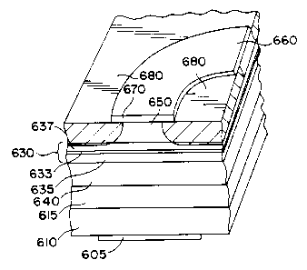
Fig. ~ is a simplified diagram of a laser device 6a0 made
~xsing,the forgoing technique. The device, on Gars substrate
and buffer layers 610 and 615, includes an active region 630
between AlXGal_xAs confining layers 640 and 650, of opposite
conductivity types. The active reg~:on includes the quantum
well 633 between undaped AlXGa1_XAs waveguide layers 635 and
637: The diagxam also shows the curv~d top contact stripe
660, the underlying GaAs cap layer 670, and bottom electrode
605: As noted a.n the f~regoing description the native oa~ide
of this exa~tple, 680', extends through the entire upper
confining layer G50 and slightly into the upper waveguide
layer 637.
Inthe description in conjunction with Fig s 1-6, the
native oxide of aluminum extends thr~ugh the entire upper
confiding layer of the laser diode and even, to a small
~'
extent, znto the waveguide region. Applicant has discovered
:that effective optical confinement; 'taile~red to obtain desired
operating conditions, can be achieved with a thick (generally,
about 3000 ~ or more) native oxide that does not necessarily
extend through the entire confining layer. Generally, a
native oxide that extends through at least one-third of the
canfin.ing Iayer is preferred. Fig. 7 shows an~embodiment of
. . ] 93/2051 ~ ~ ~ ~ ~ $ ~ ~crrus9~roz~aa
17
the invention having a linear stripe 760 and wherein the thick
oxide 780 is controlled (e.g. by controlling the time of
exposure andlor temperature in producing the native oxide) to
extend about half way through the upper confining layer. In
this example, the aluminum fraction (x) of the AlXGa1_XAs
confining layers 7~O and 750 is relatively low, for example
about 0.4, which results in lower vertical (i.e., in the
direction transverse the layers) confinement of the laser
beam. (Layers with like reference numerals to those of Fig. 6
represent similar structure.] As described further
hereinbelow, less vertical confinement permits greater
expansion of the beam into the confining layers and,
accordingly, a larger effective lateral refractive index step
encountered by the beam as a result of the native oxide in the
Confining layer.
Reference can be made to the following publications which
relate, inter alia, to control of the optical (field and gain
profile by adjusting the thickness of native oxide outside the
active strige and to control of oxide thickness to determine
the degree of optical eonfinemen~ts
F:A. Kish, S:J. Carac~i, 1~. Holonyak, Jr., J.M.
Dallesasse, K.C. Hs~.eh, M.J~ Raes, S.C. Smith, & R.D. Burnham,
°'Planar Native-Ox~.~le Inde%-Guided AlXGa~_XAs-GaAs Quantum Well
Heteros~ructure Lasers", Appl. Phys. Lett. 59, 1755, September
30, 1991;
F:A. Kish, S.J. Caracci, N: Holonyak, Jr., and S.A.
Maranowski, J.Nt. Dallesasse, R.D: Burnham, and S.C. Smith.
t,~~sible Spectrum Idati~re°-O~ide Coupl~cl-Stripe Ino.~(Al~Ga~-x)o.~P_
In0.5~a0.5P Quantum Well , Heterostructure Laser Arrays'" , Appl .
Phys.~ Lett. 59.2883, November 25r 1991; ,
FA. Kish', S.J. Caraeci, ~T~ Holonyak, Jr., P. Gavrilovic,
K. Meehan, ~ ~.~~ William, °"Coupled-Strfipe In-Phase Operation
Of Planar Native-Oxide Index°~ua.ded AlYGa~_yAs-GaAs-InXGa~_XAs
Quantum-Well Hfetex'ostructure Laser Arrays", Appl. Phys. Lett.
71e J~IriuaY'~r 6, 1992;
F.A. K sh, S:J« Garacci, S:A. Maranowski, N. Holonyak,
~'r,, K.C. Hsieh, C:P. Kuo, R.M: Fletche.r, T.D. Osentowski, &
PG'f/tJS93/02~:. ~>
Wo 9~~2~''3 2 9 ~ ~
18
M.G. Craford, "Flanar Native-Oxide Buried-Mesa AlxGa1lxAs-
Ino.S(AlyGal_~)o.sP-Ino.a(AlZGa1_Z)o.sP Visible-Spectrum Laser Diodes",
J. Appl. Phys. ?1, 2521, March 15, 1992.
Fig. 8 illustrates a passive curved waveguide in
accordance with a form of the invention. The waveguide, which
can be coupled (directly, or evanescently) with a suitable
light source [not shown], includes, for example, GaAs
substrate and buffer layers 810 and 815, and an AlxGa1_xAs (x =
0:8; for example) waveguide layer 820. The GaAs cap layer
870, native oxide confining regions 880 (which extend about
half way through the alumanum-bearing material in this case),
a~ad the contact stripe 860, can be formed using the previously
described techniques.
Figs. 9-18 illustrate configurations of lasers or
waveguides (cross-sections of which may be, for example, ,,of
the-types shown in Eigs. 6, 7 and/or 8) that can be
advantageously implemented utilizing the principles of the
invention. In these Figures, the white regions represent
.either the laser stripe configuration, which has thereunder,
aster axia, a waveguide reg~.on with he index of refraction
confinement in accordance with the Present invention or, in
the case of a waveguide, the index-confined waveguide region
in accordance with the princ~.ples hereof; Figo 9 illustrates
a ring configuration, wi h light energy travelling in bobh
directions. Fag. 1,O illustrates'a quarter ring, with light
energy again travelling in both directions. This
configuration, in an active or a passive device, can be
utilized to obtain a ninety degree change raf direction of the
light path. Figs 11 and 12 illustrate ring laser or
waveguide confi~gu~ations with tangentially coupled branches.
In Figs 1~ and 14, mul i-stripe lasers are shown as being
coupled by'ring lasers, such as for phi a locking. The stripe
spacing can: be substantial. Fig. 16 shows a similar
arrangement, but with half-ring lasers, and Fig. 15 shows a
series of coupled half-rings. Thelocking or tuning provide
by these configurations'can result in enhanced longitudinal
and/or transverse mode-operation. Fig. 17 shows curved
3 93/20581 ~, ~, J ~i ~ ~ ~ PC.'f/USg3/02$44
19
sections in an "S-bend" arrangement for providing an active or
passive lateral offset of the optical beam path. Fig. 18
illustrates the surface configuration of a laser or waveguide
which couples light in a single branch with four curved
branches.
In a further form of the invention, a quantum well
heterostructure is grown by metal-organic chemical vapor
deposition [°'MOCVD"] on an n-type GaAs substrate. After n-
type buffer layers of GaA~ ( ~0.5~um) and an Alo,z3Gao_~7As ( - l~cm)
payer, an AIo.~Gao.SAs lower confining layer is grown to a
thickness'of - l:Sum: The active region of the quantum well
heterostructure is,then grown, and includes a -- 2100
waveguide region of undoped Alo.z3Gao.~7As with ~ 100 ~ undoged
~aAs quantum well (QW) grown inside the waveguide region - 700
~, fram the lower confining layer. An upper confining layer of
p-type Alo:eGao.2As 1,s grown to ~ thickness of about 3500 ~, a:~d
a heavily doped p-type GaAs contact layer is grown thereon,
the contact payer having a thickness of about 800 ~.
The position of QW is displaced from the center of the
wraveguide for more effective overlap of the high-gain region
with the optical mode, which is displaced towards the
substrate due to the asymmetric confining layers. This
asymmetry is purposely introduced to minimize the effects of
thensurface of the laser crystal (located - 3500 ~ from°the
'waveguide) ~y shift~.ng the optical field toward the substrate.
The shallow upper confining'layer is desirable in order to
m~:n~:mize current spreading, allow finer pattern definition,
and'improved heat dissipation with the crystal mounted p side
''d~wn" and thus the. active region closer to the heat sink.
The thin upper confina.ng layer structure combined with ~.he p-
type metallizatiorimay also serve to reflect light emitted
toward the surface back into the crystal for improved device
properties. [~ laser diode, fabricated using the described
type of QW heterostruc~ure, and comprising a linear array of
small rectangular 3.nternal coupled cavi ies delineated by
oxidation of the high-gap AIxGaI~XAs upper, confining layer, . is
described in NEl--rein, F.A. Kish, N. Holonyak, Jr., A.R.
~ f.r f-. 7 71F7 L
,rwF r~...:n : a0.". 4
s»-irrvT.i7=-Y f ' o
i .°. aio r
a . rt t f.
x,., < r- s .a .e, d .. , a . :. G- . . ..
. . . , r x.. . > ... ,. . . ° a.. « .. I : 'a
_... _ ___.._ . ......,.. .... . .....,..... ~n,.. ....~x , . . . .. .... . ,
. ,. . a r. ,.-i ,.. . . ... . ... , ,~ ... ., w27 s. . x. m.. ,4., .. ,.w .,
. ... a _ . , .<.. ., n_ , a.. s.. .:"~. , . . ,... 2~.e~.w
w~ ~3i2oss~ . Pc-rms~3~o~a~a <r
Sugg, M.J. Ries, S.C. Smith, J.M. Dallesasse, and R.D.
iBurnham, "Native-Oxide Coupled-Cavity AlxGa~_XAs-GaAs Quantum
Well Heterostructure Laser Diodes°', Appl. Phys. Lett. 59,
2838, November 25, 1991.]
A laser diode array in accordance with an embodiment
hereof is fabricated by patterning - 1Ø00 ~ of Si3N4 into
repeated (masked) rectangular cav~.tie's (- 19 um long, - 4 Nm
width, ~ 3 arm end-to-end spacing), which axe arranged
lengthwise in two parallel stripes with - 1 Nm separation.
The exposed GaAs cap is then removed by chemical etching
(HZS04:H202:H20, 1:8:80) and the crystal is placed in an open-
tube furnade (supplied with a N2 carrier gas bubbled through
HzO at 95°C) at 425°C for 20 min: As above.,,,, this process
results in he transformation of 1300 A of the Alo.eGao.zAs
upper confining layer to native oxide outside of the repeated
cavities. The S13N4 is then removed in a CF4 plasma. The
inset-of Fi.g: 19 shows a photomicrograph of the surface of the
crystal after these processing steps. In order to increase
the doping ~:n the rectangular GaAs contact areas, the crystal
is sealed xn a.n'evacuated quartz ampoule and is shallow Zn-
diffused (ZnAs2;source, 540°C for 20 min), The crystal is then
lapped and Qolished (on'the substra~.e side) to a thickness of
100 ~t~n, and is metalli:zed with Ti°Au across the oxide and
the g-type GaAs "contacts" and with Ge~Ni-Au on the n-type
substrate side. The. sample is then cleaved into 250-500 um
wide Fabry-Perot resonators, diced, and indiv~.dual dies are
mounted'p-side downon Ih°coated Cu'heat sinks for continuous
,(cw) operation.
The unusual switching behavior of the resultant 2-D
stra.pe lasers i~s evident from the L-I characteristic shown in,
Fiq: 19, which, after reaching ~ peak ire power of - 12.5 mW at
(a) 115mA, decreases over 50$ in power from (a) 115 to (b) 150 _
mA, and simultaneously shifts its single mode operation (Fig.
20) to longer wavelength. At (c) 164 anA (Fig: 20) the single ,
mode operation of (a) and (b) has switcfied off, and in the
braad spectrum of (c) 164 mA the resonances of the 19 Nm long
minicavities are evident and marked with straws. In the broad
.~. . ,
.!
a
5:
.-i
. a::.. . . F
,a..o
-,r- ;: .5 6
., a ...
rc... .y
3v
f Y ,:!"
x. ,:.
<.,.
<.r"t"'.'. T r. ,.-a
r , " r. .; - Y. .
n.wi f :: l... us. ' r rt%:
t. , . 14 .
n a~ H.
.f .,b.. ~. ,..
hk.J.t. t'.. ~.Y.:
" q . ::."7
~~y , t I a '.I Y ~t..
." f ~r
.Y . ~ :;.
r 't, ..
:'/l 5',~.. Y-..t 't. ..' h..t'.
. .~.. a.. ,. x' 3. ., 3 A . . .
t.,. a. . . .. v., . . , , > . .w r ., . . t Y n. .t .N. .. ..
a~,~ ~A~X, ~. .. .. n. . . .. . .. .: ~;."t. . . ..t.::. : ~r:'~...... ,
m.,... , , ..,. ~ t .:c.r.. ... . _.. .. .., ,. . . ,~....',. f ...,.. , ..: ~
°rs.~ ~ .. .. . .. . .... ....,. .., .. " . ,.. " , ... _ ,..... .., ._
_ ..,..
~" ~i X312~581 , ~ ~ ~ ~ ~ P~'f/US93J02844
21
spectral region of weak stimulated emission, the minicavities
tend to store photons, making the mode amplitudes (marked with
arrows) smaller (c of Fig. 20). Note that the mode structure
near the peak of the spectrum in (c) is sufficiently
complicated that it is not evident that at (b) 150 mA the
single mode laser operation has shifted fully, from (a) 115mA,
to a minicavity resonance (e.g., bhw - 6 meV vs. DE ° 9 meV
fr~m resonance to resonance). It is evident from (a) to (b) to
(c) in Figs. l9 and 20, however, that single mode operation is
turning-off and mufti-mode operation, and weaker stimulated
emission, is turning-on as the current is increased.
The unusual switching behavior of these 2-D array QWH
stripe laser diodes is much more evident in Fig. 21. The L-I
characteristic shows that, with increasing current, the laser
turns on and off twice. As shown by the inset, which
corresponds to the peak Uf the L-I characteristic (> 12 mW,
415 mA, anarked); single mode operation still occurs. In the
valley region between 220 and 300 mA, broad-spectrum multi-
moda operation similar to that of Fig. 20(c) occurs (data not
shown). As the dashed line of Fig. 21 shows, the emission
intensity an this region:-is at or somewhat above spontaneous
em~.ssic~n. Most of the 2-D array lasers examined behaved as
Shown 3.n Fig. 21.
The data of Fig. 22 show in some detail the behaviar of
the di~de of Fig. 21 near he diamond°shaped point located at
mA on the L-I characteristic. For comparison, at (a) 40
mA in the spontaneous regime ttie near field (NF) exhibits two
intensity peaky expected of a twin linear array, with the
spacing of ~.2 um agreding with the 2-D array width shown in
he inset c~f' Fang. 19: At (b) 71 .mA the near field still,
exhibits twin a.ntensity peaks; and the spectx'um a single main
mode corresponding to the left NF peak and significant
satellite longitudinal modes corresponding to the right NF
peak. A small current change of 1 mA (71 ~ 72 mA) produces
abrupt switching: The satellite longitudinal modes (Fig. 22c)
vana.sh abruptly, and simu~.taneously the right NF emission.
peak: It is clear that the strong coupling of one side of the
»~~,,.
-,..: -,.. , "<.::;: , .; ".; .; ,.. :; :~: ,. . . . .. ; .... _,...
r"i h v
~Yt7 93120581 PCT/US93/02844 :, F
~~~2g~6
zz
diode interferes, constructively or destructively, with the
other side Uf the diode. Also it is evident that the manner
in which the current has been partitioned among many identical
coupled rectangular minicavities insures that the resonant
operation between the cavities is favored.
The data of Figures 19-zz demonstrates a laser diode
having two parallel linear arrays c~f.'small coupled rectangular
cavities delineated by oxidation of the high-gap AlXGaX_lAs-GaAs
QWH. The two dimensional laser array exhibits mode switching
and switching in the L-I characteristic with increasing
current. Depending on the bias position (current) on the L-I
curve, the laser operates in a sinc3le longitudinal modes in or
near the spontaneous regime. For example, the resonances of
the minicavities are evident in the spontaneous spectra in
spite of small heating effects and carrier-induced changes in
dielectric properties. As above, optimization of the
geometry, sire, and number of the minicavities, and their
coupling, may result in improved behavior of these devices.
In another form of the invention, described beginning
with Fig. z3, the QW hetero~tructure crystal is substantially
the same as the one described above in conjunction with the
previous device. In'the present embodiment; the laser diode
array 3s fabricated by first depositing 1000 ~ of Si3Na on
the crystal surface, which is then patterned into end-to-end
reputed (masked) rectangular cavities (minicavitzes, 6 pm
wide and 19 p~m long on 2zpm centers) arzanged lengthwise.
Next, 6 ~m p~~otQresist (PR) Stripes ire patterned - 5 ~m away
from the linear array of mina.c~vities: The patterned PR and
Si3Na then serve as a mask for the chemical etching
(HaSOy~~2Oa:H20, 1:8:80) of the GaAs cap layer, leaving the
~iigh-gage AlXGa1_XAs exposed outside of the patterned regions ,
The PR is then removed and the sample is placed immediately in
an epen°tub~ furnace (~z5°C) supplied with H20 vapor in an N2
carrier'gas for z0 anin. Again, this process results in the
conversion of the exposed ~~.gh-gap A1XG~1_XAs to a low-index ( n
1.6) insulating nativeoxide looted ~ 1000 A above the QWH
waveguide region. The patterned 5i3N4 and unetched GaAs
~n~r 93f20581 - ~ ~ ~ ~ ~ ~ ~ P~lffllS93/02844
23
regions are unaffected by this treatment. The patterned Si3N4
is then removed in a CF4 plasma. The inset of Fig. 23 shows
the surface of the device after these processing steps. Next
the sample is ~n-diffused (540°C, 20 min) to increase the
doping in the contact regions (labeled "GaAs" in Fig. 23)..
The crystal is then lapped and polished to a thickness of --
125 um and, again, metallized over the entire top surface with
Ti-Au for p-type contacts and with Ge-Ni-Au for n-type
contacts. Finally the crystal is cleaved, diced, and
individual dies mounted on In-coated copper heat sinks for
continuous (cw) operation.
The large amplitude switching praperties of the single-
stripe laser coupled to the active linear array are shown by
the 300 K continuous (cw) L-I curve of Fig. 23. The laser
threshold current is 32 mA, and laser operation persists;up to
a current of 168 mA. At this po~.nt the diode switches
abruptly from stimulated emissi~n, ON (19.6 mW/facet,
undoated), to the spontaneous regime, OFF (0.4 mW/facet,
uncoated). This behavior corresponds to a large ONaOFF pawer
~rati~ c~f 4g: These ara inherently nanlin~ar devices, and
exhibit bistable operation with a large hysteresis. As the
current is decreased (returned) to 123 mA, the diode switches
back from the spontaneous regime, OFF, to the simulated
segue; ON. For further current ~.ncreas~ beyond 168 mA,°after
the dev3;ce has switched OFF with increasing current, only a
slight increase in the spontaneous output is observed until
fai3ure at 18? mA. 'We mentir~n that, although hysteresis
occurs in the LaI characteristics, no hy~t~resi is observed
3n the current versus voltage (i-V) ch~racteri~stics of these,
devices: ;;
The L,-T characteristic (cw 300 K) of another diode
exhibiting similar switching behavior is sh~wn in Fig. 24.
The laser threshold current is 2? mA, with the device
exhi;bit'a,ng essentially a single ~ 5.5 pm~wide Gaussian near-
f3eld pattern (data not shown). This intensify pattern
corresponds to laser operation of the ~ 6 um wide uniform
stripe (inset of Fig. 23); which is expected to reach
WO 93/205S1 PC'f/U593/02R44 i~ ~~ -a
~~ ~ s~ :~
24
threshold before the segmented linear array. From gain-loss
considerations, the linear array with its repeated unpumped
absorbing sections should have a higher laser threshold.
Throughout the entire operating., range, a single-stripe
near--field gattern persists, i.e.; only very weak output is
observed from the linear array~.portion of the device. The
near-field pattern (300 K, cw.,bperation) at (a) 99 mA just
before the switching from ON to OFF, i.e., before switching
fram single-mode stimulated emission to spontaneous emission,
is shown in the inset of Fig. 24. Similar to operation just
abave threshold, only a 5.5 Nm Gaussian near-field is
observed at significant amplitude. After the diode switches
OFF at (b) 100 mA, no pattern is observed on the same
sensitivity scale of the CCD detector. However, at higher
sensitivity (11.3x), emissi.an from the same aperture (- 5.~
Nm) ~:s observed (b'). Thin near-field pastern also is
observed as the laser is switched back from OFF to ON. These
data indicate unambiguously that only the uniform laser stripe
prouides much of the optical'output of the system. The side-
coupled linear array serves mainlx to effect the interferences
and swit~hing~ ON°OFF, and does not contribute primarily to
the optical output;
Further understanding of the operation of these diodes is
obtained by'examining the output spectra. Somewhat above the
threshold at 30 mAr the diode of Fig. 24 operates in a single
longitudinal mode (~ 8353 ~. data not shown). This behavior
eantinues to the peak of the L-I curve'of Fig. 24 (63 mA),
where the single mode operation "hops" to longer wavelength
g367 1~, data not shown). :Throughout the entire stimulated
emission operating regime (,30 -~ 99 mA), the output occurs in a
well developed single longitudinal made. For example, at 63
mA the 'laser exhibits aside-mode suppression of 29 dH. The
:mode hopping, and corresponding structure in the L-I curve
(Fig. 24), is attributed. to the interaction (interference) of
the single laser str~.pe with side-coupled active linear array
and its resonances and stop hands.
Longitudinalmode spectra in the higher-current switching
"'i> 93/2~158a PCT/US93l02844
regime of the device of Fig. 24 are shown in Fig. 25.
Immediately before switching from ON (stimulated emission) to
OFF (spontaneous regime), (a) in Fig. 24, the laser operates
in a single longitudinal mode at ~, w 8415 A, which is shown
as (a) in Fig. 25. When the diode switches OFF to the
spontaneous regime, (b) of Fig:. 24, the longitudinal mode
spectra appear as shown in (b) of Fig. 25. At this point, the
output consists of the spontaneous emission of the single
stripe laser (group of lower energy modes) and the linear
array (group of higher energy modes). The coupling of the
linear array to the stripe laser leads to interference. The
resonances of the minicav~ities of the linear array are
apparent (clearer in the laboratory data) at higher energy in
the spectrum of Fig. 25(b) and are marked with arrows. The
spacing of these resonances (~~1 - 50 .~) corresponds to the -
19 um minicavity length shown in the inset of Fig. 23. It is
noted that the output in the OFF spontaneous regime (Fig.
25(b)) differs s~.~nificaratly from that observed in the
spontaneous regime below laser threshold (< 27 ~1), where only
the longitudinal mode output of the single laser stripe (group
'of lower energy modes) is observed (data not shown).
Tg~~ described switchihg and storage are fundamentally
different from previously ~~Qo~ted switching laser devices.
The 0~-O~'F switching behavior occurs in this embodiment sn a
single unbroken or uninterru~ated laser stripe. The switching
behavior is owing to the influence (via sidewise coupling) of
an active 1'inear army. The switching and bistability is
effected by the periodic structure ~f the,linear array (see
~i.G. Wiriful, J,H. Marbuxvger, and'. Carmir~s Appl. Phys. Lett.
35,; 3,79 ( 1979) °,, Jr ~e and M: Cada, IEEE J. Quantum Electron.
QE°27, 1182 (1991)) and the obvious inhomogeneous carrier
distribution, aa~d i.nhomogeneous operation, resulting from the
nativ~--oxid~ patterning of the gray.
Thus, this embodiment sets forth a new form of optical
switching element in which a conventional single-stripe laser
is side-coupled to a linear array of coupled minilasers. The
resulting many-eleanent twin-stripe laser is easily realized
CA 02132986 2003-04-22
WO 93/20581 PCT/US93/02844
26
via native-oxide device processing. The planar devices exhibit
large hysteresis in the L-I curve, with large amplitude switching
from the peak of the stimulated emission regime (ON) to the
spontaneous regime (OFF). Changes in the coupling, e.g., the
spacing between the laser stripe and linear array and between the
array elements, a.nd in the geometry of the structure should
improve the switching l;~ehavio:r of these lasers. Independent
control of the current (carrier population) in t:he single laser
stripe in the linear a~°ray, e.g., via a third terminal electrode,
should allow control o:F the switching behavior, and other
variations are possible.
Fig. 26 shows a part of the surface of the device described
in conjunction with Fi~~ures 23-25, and is used as a reference to
show the cross-sections used for the illustrations of Figures 27-
29. In Figure 26 the stripe is labelled 1210 and the
minicavities, or porticans thereof, are labelled 1221-1225. The
cross-section 13-13 is taken through the stripe 1210 and an
adjacent minicavity 12'..4. The illustrated layers, which were
previously de:acribed, include the bottom contact metallization
1250 (it bein<~ understcaod throughout: that references to "bottom"
or "top" are ?°or ease c:~f description, as the device may be
mounted and used in an~,r desired orientation), followed, in
ascending ordE~r, by the:':ntype GaAs substrate layer 1255, the n-
type GaAs buff=er layer 1.258, the n-type A1o.23Gao.,.,As buffer layer
1260, the n-t~rpe Alo.SGa.a.SAs lower confining layer 1262, and
active active region 1:?70 that includes a GaAs quantum well layer
1271 between waveguide layers 1273 a.nd 1275 of undoped
Alo.z3Gao..,~As. r~.bove the active region is the upper confining layer
1278 of p-type: Alc,_BGao,;,As. The layer thicknesses may be, for
example, as previously indicated above for the experimental
device. The p--type GaAs contact 1281 and the p-type GaAs contact
1283 respectively define the contact positions of the stripe 1210
and the minicavity 1226: of Fig. 26. The native oxide is shown at
1291, 1292, and 1293, a.nd, in this example, has a thickness of
about 1300 ~ The oxide a:Lso extends somewhat under the GaAs
contact regions. The top (p-side) metallization is labeled 1240.
CA 02132986 2003-04-22
WO 93/20581 PCT/US93/02844
27
The diagram of F:~.g. 28 illustrates the cross-section
defined by arrows 14-14 of Fig. 26. In this view, only the
contact region 1281 of t:he stripe 1210 is visible. The oxide
(1294) extends continuously to the :right of the stripe.
Fig. 29 shows the cross-section defined by arrows 15-15 of
Fig. 26. This view is longitudinally through the minicavities,
with two minicavities being shown between three oxide regions
1296, 1297, 1298. The :longitudinal dimension of the contact 1283
is seen in this view.
In the illustrated embodiments, operation may be "two
terminal", such as by applying the electrical potential between
the bottom electrode and the top common metallization. The device
can alternatively be made for operation as a three terminal or
multiple terminal devic::e. For example, Fig. 30 illustrates a
device having a stripe 1610 with mini cavities 1620 on both
sides, each line having a common metallization (represented by
the joining lanes between minicavities) and its own terminal, so
that the device can be operated with four independent terminals,
with three terminals (~:or example, t:he terminals of only two
adjacent line, and the bottom terminal, or with the two outside
lines in common) or twc:a terminals, with all three lines in
common. [In this diagram, and in other diagrams hereof where a
plan view of the minicavity and/or stripe configuration is shown,
the underlying structure is of the type previously described, the
fabrication m<~sking pat::t~erns being consistent with the structures
illustrated.) Fig. 31 ~.llustrates a two-dimensional array o.f
adjacent liner of mini cavities, with individual terminals
coupled with the mini cavities. It will be understood that a
terminal can be coupled with any desired combination or group of
cavities or m_Lnicavitie:~s.
The previous embodiments illustrate straight line
minicavity and stripe c.~.onfigurations, but it will be understood
that the principles of the invention also apply to minicavities
and stripes arranged in curved line
r.."'
1~J0 93/20581 PCflUS93/02844 <:'
- 28
configurations and arrays. Figures 32-39 illustrate some
representative embodiments (with bottom electrode and various
possible top electrodes not shown). In Fig. 32 there is shown
a ring laser which is divided into curved minicavities 1815,
to obtain the types of effects described in N. El-Zein, F.A.
Dish, N. Holonyak, Jr., A.R. Sugg, M.J. Ries, S.C. Smith, J.I~.
Dallesasse, and R.D. Hurnham, "Native-Oxide Coupled-Cavity
AlXGa1_xAs-GaAs Quantum Wel l Heterostructure Laser Diodes °' ,
Appl. Phys. Lett. 59, 2838, November 25, 1991, in the context
of a ring laser. [It will be understood throughout that any
of the curved configuratibns need not be precisely circular,
that any desired portions of rings or curves can be used, and
that the rings or portions thereof can be cleaved at any
desired position to obtain one or more outputs.] Fig. 33
illustrates two concentric ring lasers, each divided into
minicavities 1915, so that lateral coupling can be achieved,
as first described in conjunction with Figures 19-22 above for
the case of straight line arrays. I~ Fig. 34, one of the
concentric rings 2010 is continuous, and the other is divided
into minicavities 2015, to ob~air~ a curved version of the
embodiment described in conjunction with Figures 23-29. Fig.
35 i.I:lu~trates a ~a.reular configuration with sector-shaped
minicavities 21.5 separated by xa$ial "spokes" of native
oxide:
Fic3. 36 shows s rung laser 2210 laterally coupled with a
stripe laser 2220, In Fig. 37 the ring is divided into
mihacavl,ties 2315, end in Fig. 38, the stripe is divided into
minicavities 2415. In F3.g.-39, both the ring and the stripe
are divided into minicavit3es (2515 and 2525, respectively).
It w~.ll b~ understood that'the previous indicated
variations with regard to numbers and types of striges, array
elements, and/or terminal connections are applicable to
embodiments with curved lines or minicavities.
Fig. 40 illustrates, in cross-section, a form of the
invention 4ahich couples cavities with d~.fferent longitudinal
mode characteristics, in the form of a vertical cavity laser
array. vertical cavity lasers are well known in the art (see,
~~~~~'~ 93/20S81 ~ ~ ~ ~ ~ ~ ~ P~.°T/US93~a2~4
29
for example, H. Soda et a1. Japan J. Appl. Fhys. 18, 59 {1979)
and K. Iga et al., Electron Lett. 23, 134 (1987), and include,
as in the lefthand unit of Fig. 40, a bottom contact 2610 on a
substrate {e.g. GaAs 2605), an n-type superlattice 2620, an
active region 2630 that includes a quantum well layer 2632
between waveguide layers 2634 and 2636, a p-type superlattice
2640, and one or more contacts 2650. Various materials may be
used. As one example, the superlattices may comprise a number
of alternating layers of AlAs and GaAs [ or AlxGa~_XAs and AlYGaI_
yAs, x~y, gr combinations of AlXGa1_xAs and conductive
dielectric stacks ( a . g . Ti02/Si02, ZnSe/CaF2 ) ] , and the act~.ve
region may comprise . Aln.lGao,9As { or GaAs ) waveguides layers with
a GaAs { or Ino,lGao.9As ) quantum well layer with total thickness
of typically - 250 ~. The contacts at the surface may
comprise for examgle Au or Ag with a standard (e.g. Ge-Au)
backside (substrate) side contact. A two-dimensional vertical
davity coupled array of such devices is described for example
in I~.G. Deppe, J.P. Van der Ziel, Nasesh Chand, G.J. Zydzik,
and S,N.G. Chu, Appl. Phys. Lett. 56, 2089 (1990). Briefly,
in operation, the multiple reflections from the superlattice
interfaces provide a relatively short effective cavity length
(typically ~ Sum) from the limited thickness device, and the
cavities are coupled wanescen~ly:
In accordance with a feature of a form of the inven-~ion,
adjacent vertical cavity laser aanits are pr~v~.ded with active
reg.ion~ of d~.fferent thickn~sses, as illustrated in Fig. 40,
where the active region 2630' is substantially thicker than
he active region thickness of its neighboring unit. In the
illustration, the quantum well layer is c~ntinuous through
adjacent active regions, although this is not necessary., The
t.v name ~s'true of the superlattice layers above the active
region 2630'. Variation o~-the upper ~r lower superlattice
thidkness laterally varies the effectide lateral mirror
areflecti.vity. Such variations may also be employed with a
uniform thickness active region to achieve local variations in
the cavity structure. In addition to the Standard evanescent
coupling, other schemes may be employed to'couple such devices
W~ 93/20581 ~'Cf/US93/02844 'i~.,.~~;
such as varying the mirror (e.g. superlattice) angles to
directly reflect some of the light from one cavity into
adjacent cavities.
There are various other techniques that can be utilized
to obtain adjacent vertical cavities having substantially
different effective vertical cavity lengths, so that lateral
coupling thereof can be advantageously exploited to obtain
properties such as switching, bistability, andlor tuning. [As
used herein, vertical cavities having substantially different
effective cavity lengths means that the cavities have
substantially different longitudinal mode characteristics, as
previously defined.] For example, the active regions of
adjacent units may comprise different materials. Another
alternative is to provide adjacent units with superlattices of
different thicknesses, or superlattices of different
configuration: An exam~lQ of the latter would be to provide
one unit having superlattices of alternating 100 ~ GaAs and
Al~s layers and the other unit with superlattices having
alternating 200 ~1 Gags layers and 100 A AlAs layers, which
results an different effective cavity lengths.
Fag. 41 illustrates a checkerboard-type array of such;
units, with the cross-hatched units representing the units
having tie thicker active regions. The array can be operated
as a two terminal device, with the top contacts coupled in
common, and potential applied between the top and bottom
c~ntact, or can be driven as a three termznal or multiple
terminal device with wparate connections to contacts.
Various other shapes and configurations in one-dimension or
wo~-dimensions can be utilized. 'In one example of fabricating
an arrays the growth may; be terminated at the active region
(2630'). A two-dimensional pattern (e.g,. a checkerboard) is
then masked using standard photolithography techniques and the
sample is subjected to chemical etching to remove a portion of
he active region (2636) in the unmasked area. This process
results in a lateral variation in the active layer thickness.
The photoresist is then removed and the upper p-type
supperlattice is grown on the patterned active region, such as
,,
». . ,...-. .. .; . .. -,:. , ;; ., ,...:. ..::.., >..:... : . . ..
P~'/US93/02844
93/20581
31
by MOCVD or MBE (molecular beam epitaxy). A circular (dot)
metallization can then be applied on the upper p-type
supperlattice for contact and reflectivity purposes.
The invention has been described with reference to
particular preferred embodiments, but variations within the
spirit and scope of the invention will occur to those skilled
in the art. For example, while the aluminum-bearing III-V
semiconductor material aluminum gallium arsenide has been
described in embodiments hereof, it will be understood that
the devices and technique hereof can employ other aluminum-
bearing IIr-V semiconductor materials, such as indium aluminum
gallium phosphide, indium aluminum gallium arsenide, or
aluminum gallium phosphide. [Reference can be made to F. ICish
et al:, J. of Appl: Phys. 71, T5 March, 1992.] Also, it will
be understood that the indicated confining layers can be;
multiple layers, one or more of which comprises the aluminum-
bear~.ng III-V semiconductor material. It will further be
unders~odd that devices can integrate the aluminum-bearing
III-V semiconductor material (from which the native oxide is
formed)ywitka other nQn-III--V semiconductor materials. It will
also b~ understood that laterally coupled cavities as
described herein can be utilized for tuning as well as
indicated functions such as switching. The lateral coupling
described herein is particularly facilitated by using the
native oxidE formed in an aluminum-bearing III°V semiconductor
material to separate laterally coupled cavities. In some of
the-configurations hereof, 5:ess gre~erred cavity definition
can alternatively be implemented by,tedhniques such as
'muZ:'~iple regrowths/overgrowths, etch and xegrowth/overgrowth:,
r~,d~geiFormation, ridge formation and overgrowth, impurity
induced layer disordering, and proton implantation.