Note: Descriptions are shown in the official language in which they were submitted.
CA 02133073 1999-07-OS
f
1
Title
Fast bidirectional analog switching system for HF
pulses of high instantaneous power.
Technical field
Switching of wide band pulses
Switch using semiconductor devices (H03B 11/10)
Introduction
The purpose of this system is electronic switching of
high voltage short duration monopolar pulses with very
short transition times, whose spectrum consequently
contains a great portion of high frequencies.
The operability of the system, depending on the actual
realization and on the load impedances connected to its
terminals, can reach up to 900 V and 50 MHz.
The analog switching channel permits the passing of
high voltage monopolar pulses in both directions and is
capable, until a certain voltage amplitude threshold, of
switching long duration bipolar signals, presenting in its
conducting state a notably low series impedance (in the
order of 1 Ohm).
This system applies more particularly and immediately
to systems for controlling wide band equipments which
operate with high frequency radiations and need switching
of high voltage and medium power pulses (medical echo-
CA 02133073 1999-07-OS
v r
- 2 -
graphy, non-destructive evaluation of materials) or of
pulses of high currents and high instantaneous powers
(ultrasonic lithotripsy, echographic inspection of strongly
attenuating industrial structures).
The importance of a switching system with these
characteristics is based on that it offers good services
simultaneously in various aspects that are normally opposed
to each other in the bidirectional switching devices
presently available:
- Maximum peak amplitude allowed in the switched
currents and voltages.
- Turn-on time and available bandwidth of the swit-
ching channel.
- Series impedance in the conducting state.
To this should be added the advantage that the control
of the system does not require the use of high voltage
sources.
State of the art
In analog switching applications, there has until now
been used methods based on the following devices: electro-
mechanical relays, bipolar transistors, thyristors, triacs
and, more recently, DMOS and VMOS transistors. Each of
these devices presents limitations in its functionability
when fast switching of high voltage pulses of high instan-
taneous currents is required (for example with capacitive
loads) and under wide band conditions.
CA 02133073 1999-07-OS
- 3 -
- The electromechanical relays offer an initially very
low series resistance in the connection state, but it
varies with the intensity of the current, an aspect
which degrades hastily with the use of the relays.
This makes these devices not very adequate for use in
the aforementioned applications, which generally
require the realization of several thousands of
switchings per second. To this should be added the
considerable activation times of these devices, which
in the most rapid versions are in the order of
millisecond, and also the limitations caused by the
mechanical bouncing of their contacts.
The switches based on bipolar transistors should be
controlled by means of the base current, which
. considerably perturbs the switched analog signal, and
additionally they require to use of expensive power
sources with voltages higher than the instantaneous
peak voltage which one desires to switch.
- The combinations of thyristors and triacs permit
high powers to be managed, but introduce too much
offset voltage and too many nonlinear effects [Silico-
nix, "Don't Trade Off Analog Switch Spec"-MOS POWER
Design catalog -AN77-2, pp. 6-43/6-48, Santa Clara,
California, 1983]. In addition, they present some
practical inconveniencies in high frequency applica-
tions: excessive temporal tolerances in the switching,
long turn-off time and introduction of transients
which degrade the switched signal, which very notably
reduces the corresponding dynamic range.
- The analog switches based on DMOS technology [J. D.
Plummer et al., "Two-Dimensional Transmit/Receive
Ceramic Piezoelectric Arrays: Construction and
CA 02133073 1999-07-OS
- 4 -
Performance" , IEEE Trans . Sonic and Ultrason . Vol . SU-
25, No 5, pp. 273-280, 1978] allow their integration
in reduced size chips [P. Harold, "Improved analog
switches and multiplexers bring benefits to old and
new applications", EDN. May 14. pp. 65-74, 1987];
There exists a wide range of these devices, commercia-
lized by different companies among which the following
ones could be emphasized: Analog Devices Inc.,
- Intersil, Maxim I.P., and Siliconix Inc. These devices
generally present low distortion and a good frequency
response, but in spite of the continuous innovations
introduced by different manufacturers, especially by
Siliconix, the maximum peak voltage that can be
switched is about 60 volts, and the resistances in the
conducting state are in the order of 40 or 50 ohms,
which seriously limits the maximum allowable current.
- Finally, the switching systems based on VMOS power
transistors, proposed by some authors [Siliconix,
"Don't Trade Off Analog Switch Spec" -MOS POWER Design
catalog -AN77-2, pp. 6-43/6-48, Santa Clara, Califor-
nia, 1983], allow the switching of until 10 watts,
linearly, with low ON impedance and very reduced
distortion, thanks to the purely resistive characte-
ristics of the drain-sourse channel. However, they
only permit the switching of positive pulses, as they
practically turn into a short circuit for negative
voltages from -0.6 volts. Some solutions to this
problem involve several VMOS transistors in relatively
complex circuits which notably raises the costs of the
switching process, especially in multichannel type
applications (Acustical Imaging, Ultrasonic Tomo-
graphy), [J.F. Gelly and C. Maerfeld, "Properties for
a 2D Multiplexed Array for Acoustic Imaging", IEEE
Ultrasonics Symp. Proc., pp 685-689, 1981; D.W.
CA 02133073 1999-07-OS
- 5 -
Fitting et al., "A Two-Dimensional Array Receiver for
Reducing Refraction Artifacts in Ultrasonic Computed
Tomography of Attenuation", IEEE Trans. Ultrason.
Ferroel. Freq. Control, Vol. UFFC-34, No 3, pp. 346-
356, 1987]. Even though this type of switches can
control fairly high currents (thanks to their low ON
resistance), they present limitations similar to those
of the switches based on DMOS transistors in what
regards the maximum switchable voltage and the
necessity of bias sources with voltages superior to
the peak amplitudes of the pulses which are to be
switched.
Brief description of the invention
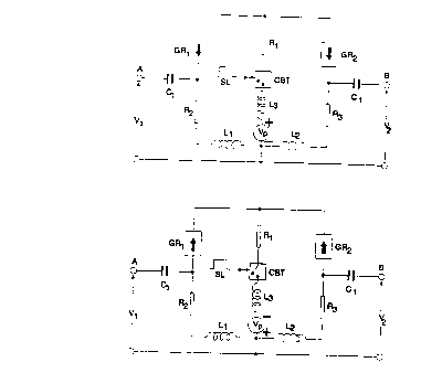
The basic principle of the procedure object of the
present invention is outlined in figure 1, in which two
functional diagrams are shown which solely differ in the
polarity of the power source which produces the voltage VP,
and in the orientation of the rectifier sets GR~ and GR2.
The main conductor channel A-B for the switching of
the power pulse is formed by the connection in series of
two high voltage capacitors C~ and two rectifier steps GR~
and GR2 capable of tolerating high voltages when breaking
and oriented in contrary directions in what regards the
conduction of current . In the f figure, two possible conf igu-
rations of the system are presented, according to the
polarity chosen for the source VP.
The rectifier sets GR~ and GRZ can be formed by any
parallel-series combination of semiconductor devices with
rectifying characteristics; the only conditions requirable
are the contrary orientation of the two rectifier steps
CA 02133073 1999-07-OS
r
- 6 -
and, in the case of high voltage input pulses, that the
rectifiers present a reverse storage time superior to the
width of the pulse to be switched, which is fulfilled in a
great number of devices commercially available.
In the off state, i.e. when the circuit is open
because so is the switch CBT, the channel A-B presents high
impedance for any bipolar signal, V~ and VZ, connected to
any-of the main terminals of the switch.
The transition to the conducting state,is achieved by
means of closing an unidirectional current switch of
conventional type, CBT, of low voltage ( in the order of 20-
40 V), which, therefore, can be controlled by a logic
signal SL from conventional TTL or CMOS logic circuits . The
closing of the switch CBT gives rise to the passing of a
continuous current through the central branch and GR~ and
GRZ from a low voltage source VP (preferably less than 50 V)
with the adequate polarity according to the connection
chosen from the two possible ones for the rectifier steps.
This current is established through the inductance L3
(which can be omitted), the resistance R~ and the two
series networks formed by the rectifier (GR~ or GRZ), the
resistance ( RZ or R3) , and the inductance (I~~ or L2) , which
can also be omitted, corresponding to each of the lateral
branches of the circuit. Under these conditions, the main
channel A-B of the circuit allows the passing of pulses
with peak voltages much higher than VP (in the order of 100
to 800 V), as long as their duration does not exceed the
reverse storage time of GR~ and GRZ and, as long as the
conducting state lasts, of any associated signal of long
duration and low voltage with peak-to-peak amplitudes
inferior to a voltage in the order of Vp/2 (which depends
on the values chosen for the resistances R~, R2 and R3).
CA 02133073 1999-07-OS
Detailed description of the invention
The switching system, object of the present invention,
is constituted by a main conductor channel and of two
secondary polarizing low voltage circuits (for the activa-
tion of the main conductor channel) composed of three
branches symmetrically connected to the intermediate nodes
of the main channel, which is formed by the series connec-
tion of two high voltage capacitors connected to the two
external terminals of the channel, and of two rectifier
sets oriented so that their connection to the central point
of the channel interconnects the terminals of each set with
the same polarity. The voltage VP of the polarization
source in the central branch can have a nominal value at
least one order of magnitude inferior to the maximum
switchable peak voltage.
The two rectifier sets, included in the switching
channel, must have a reverse storage time superior to the
duration of the high voltage pulses switchable through
them; these groups can be formed by different combinations
of circuits with suitable rectifying characteristics, based
on semiconductors such as diodes, bipolar transistors,
thyristors, triacs or MOS transistors, grouped in series or
in parallel, so as that, by adding new components of this
type in series or parallel connection, the maximum switcha-
ble voltage or current can be increased.
The three branches of the polarization circuits
contain inductive reactances connected in series with
resistances, in order to obtain high values of input
impedance at the terminals of the switch, which makes the
application of the switch possible in multichannel type
configurations.
CA 02133073 1999-07-OS
When with the high voltage pulsed signal (typically in
the order of 100 to 800 V) is associated (in the same
pulse train or as an answer to this signal) a low voltage
one, whose peak value does not exceed a threshold value,
of an order of magnitude given by the expression
V~-VP~ ( 1+R~~Rg+R~~R2 )
the main switching channel does not present any limitation
in the temporal duration allowed for the switched signal,
i.e., the signal will pass as long as there exists a
conducting state through the two rectifier sets, even
though its duration has surpassed the reverse storage time
of them.
This feature is very adecuate for transceiver systems
such as pulse-echo systems, in which their limited pass
band gives rise to, in the reception stage, low amplitude
signals but with a duration far greater than the duration
of the pulse used for their high voltage excitation. The
bidirectional behaviour of the switch, object of the
present invention, is thus suitable for this kind of
applications.
The choice of sufficiently high values for C~, for
example 100 nF, guarantees a perfect isolation of the
switched signals with respect to the polarization circuits,
without introducing substantial distortions into these
signals. The incorporation of these series capacitors in
the ends of the conduction channel, with impedances in the
CA 02133073 1999-07-OS
t
_ g
radio frequency range several orders of magnitude inferior
to the impedances of the polarization branches and of the
switched load, makes possible the switching of signals with
very long duration as long as the total peak-to-peak
amplitude of these signals does not exceed twice the
voltage threshold V" determined by the indicated formula.
In figure 2 one way to~ materialize. the present
invention is shown in detail. The circuit shown in this
figure permits the direct control of the switching channel
by means of a control input ( EC ) activated by logic signals
of the TTL type. In this case, the current switch CBT is
materialized by means of a logic inverter circuit with open
collector output (ICA), for example 1/6 of the chip 7406,
connected through a diode D to the base of the NPN type
transistor T which, because of its polarization from the
collector through the resistance R4, supplies the conti-
nuous current necessary for activating the power channel.
The rectifier sets GR~ and GRZ are implemented by means of
two diode networks RDA and RD2.
The circuit includes the capacitors CZ (whose capacity
is at least two orders of magnitude less than the capacity
of the capacitors C~), in parallel with the input impedan-
ces Z~ y Z~. The purpose of this is to minimize the depen-
dency of the leakage currents during the non-active phases
of the main channel with these impedances.
The conductor channel C~-RDA-RDZ-C~ permits, when it is
active, the reception at terminals of the input capacitor
C2 of echo signals v~ originating from active loads Z~ ( for
example of piezoelectric type), as a response to their
previous excitation by means of the transmission of a pulse
V~ with high instantaneous power through said channel.
CA 02133073 1999-07-OS
r
- 10 -
The main advantages of the present invention in
comparison with alternative procedures are summarized under
the following points:
- Its capacity for switching high voltages, in the
order of several hundreds of volts, without using
mechanical type contacts or high voltage bias sources .
Its low series impedance during conduction, which is
not degradable during long time use, in combination
with its short activation time allows switching of
high currents (several amperes in the case of a
typical materialization) in a wide radio frequency
range, and with high pulse repetition rates.
This circuit, fitting conveniently the values of the
resistances, capacitors and inductances to the loads Z~ y
Z~, allows the control, from a low voltage source Vp, of
the switching of short impulses Ve, normally shorter than
1 microsecond, with high peak voltages and currents, which
can be adjusted optimally in each application by using a
sufficient number of diodes with appropriate characteris-
tics in each RD network.
Description of the drawings
Figure 1. Basic principle of the switching system.
A,B ........ Access terminals to the switching
channel.
V~, V2...... Voltage between the terminals A, B and
ground, respectively.
C~.......... High voltage capacitors.
R~, RZ, R3. . Electrical resistances .
CA 02133073 1999-07-OS
- 11 -
L~, L2, L3 . . Inductances .
GR~, GRZ.... Rectifier sets mono or multi- compo-
nent, connected to the resistance R~
either through their anodes or through
their cathodes.
CBT......... Low voltage switch.
VP. . . . . . . . . . Low voltage source for polarization
of
the switching channel by means of
closing the switch CBT. The polarity
(+,-) of this source is determined by
the direction chosen for the flow of
continuous current in GR~ and GR2.
SL.......... Input logic signal for the control of
the switch.
FiQUra 2. A practical realization of the invention, which
can be controlled digitally by means of TTL pulses.
V~.......... High voltage excitation pulse.
V~.......... Echo voltage received as a response to
Ze.......... Output impedance of the generator of
the pulse V
Z~.......... Load impedance.
C~, C2...... Electrical capacitors.
R~, R2, R3, R4 . Electrical resistances .
L~, LZ, L3. . Inductances .
RDA, RD2, .. Diode networks based on series and/or
parallel connections.
T........... Low voltage high frequency NPN transis-
tor.
D........... Rectifier diode.
VP.......... Low voltage source.
ICA......... Logic inverter with open collector
output.
CA 02133073 1999-07-OS
- 12 -
EC.......... Control input, adapted to TTL type
logic.
10
20
30