Language selection

Search

Patent 2133213 Summary

Third-party information liability

Some of the information on this Web page has been provided by external sources. The Government of Canada is not responsible for the accuracy, reliability or currency of the information supplied by external sources. Users wishing to rely upon this information should consult directly with the source of the information. Content provided by external sources is not subject to official languages, privacy and accessibility requirements.

Claims and Abstract availability

Any discrepancies in the text and image of the Claims and Abstract are due to differing posting times. Text of the Claims and Abstract are posted:

  • At the time the application is open to public inspection;
  • At the time of issue of the patent (grant).
(12) Patent Application: (11) CA 2133213
(54) English Title: EARTHING SWITCH FOR METAL-CLAD HIGH-VOLTAGE SWITCHGEAR INSULATED WITH COMPRESSED GAS
(54) French Title: MISE A LA TERRE POUR APPAREILLAGE HAUTE TENSION A BOITIER METALLIQUE A ISOLEMENT PAR GAZ COMPRIME
Status: Deemed Abandoned and Beyond the Period of Reinstatement - Pending Response to Notice of Disregarded Communication
Bibliographic Data
(51) International Patent Classification (IPC):
  • H02B 13/075 (2006.01)
(72) Inventors :
  • PFAFF, DIETRICH (Germany)
  • SCHMIDT, REGINA (Germany)
  • PIRCHER, CHRISTIAN (Germany)
(73) Owners :
  • SIEMENS AKTIENGESELLSCHAFT
(71) Applicants :
  • SIEMENS AKTIENGESELLSCHAFT (Germany)
(74) Agent: SMART & BIGGAR LP
(74) Associate agent:
(45) Issued:
(86) PCT Filing Date: 1993-02-26
(87) Open to Public Inspection: 1993-10-14
Examination requested: 2000-01-13
Availability of licence: N/A
Dedicated to the Public: N/A
(25) Language of filing: English

Patent Cooperation Treaty (PCT): Yes
(86) PCT Filing Number: PCT/DE1993/000189
(87) International Publication Number: DE1993000189
(85) National Entry: 1994-09-28

(30) Application Priority Data:
Application No. Country/Territory Date
P 42 11 157.9 (Germany) 1992-03-31

Abstracts

English Abstract


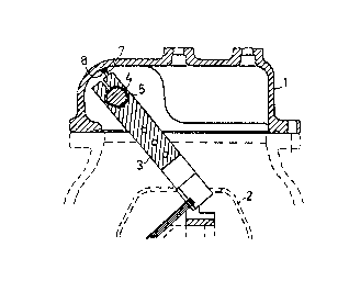
Abstract of the Disclosure
EARTHING SWITCH FOR METAL-CLAD, HIGH-VOLTAGE SWITCHGEAR
INSULATED WITH COMPRESS GAS
In the case of an earthing switch for a metal-clad,
high-voltage switchgear insulated with compressed gas,
the mobile earthing contact (3, 11) is arranged so as to
be insulated from the earthed cladding (1) for measuring
purposes. This insulation arrangement of the earthing
contact (3, 11) is bypassed by an electrical connection,
preferably outside of the cladding (1), for the function
of earthing switching device. The electrical connection
is released [disconnected] when the earthing contact (3,
11) is connected in the closed position to a measuring
device. In accordance with the invention, an additional
contact arrangement (7, 7a, 8, 8a) is provided, which is
forced to electrically bypass the insulation arrangement
and which connects the mobile earthing contact (3, 11)
to the earthed cladding outside of the closed and open
position in the course of the switching motion between
these two positions.
By this means, overvoltage resulting from
discharge occurrences on the insulation arrangement and,
if indicated, damage to measuring instruments connected
to the earthing switches are reliably avoided.
FIG. 2


Claims

Note: Claims are shown in the official language in which they were submitted.


6
Patent Claims
1. An earthing switch for a metal-clad, high-voltage
switchgear insulated with compressed gas having a mobile
earthing contact (3), which is arranged so as to be
insulated from the earthed cladding (1), and having an
electrical connection that bypasses the insulation
arrangement of the earthing contact (3), as needed, c h
a r a c t e r i z e d i n t h a t an additional
contact arrangement (7, 7a, 8, 8a) is provided, which is
forced to electrically bypass the insulation arrangement
and which connects the mobile earthing contact (3, 11)
to the earthed cladding (1) outside of the closed and
open position in the course of the switching motion
between these two position.
2. The earthing switch according to claim 1,
c h a r a c t e r i z e d i n t h a t the mobile
earthing contact (3) is a blade switching contact (3)
arranged on a rotatably driven shaft (4), which is
capable of being connected to a sliding-action contact
strip (8) of the cladding (1) arranged concentrically
around said shaft (4) via a flexible pin (7) that is
movable at right angles to said shaft (4).
3. The earthing switch according to claim 1,
c h a r a c t e r i z e d i n t h a t the mobile
earthing contact is a movable contact pin (11), which
has a straight line displacement and is connectible to a
sliding-action contact surface (8a) of the cladding (1)
running parallel to the axis, via flexible pin (7a)
movably supported at right angles to said contact pin
(11).

Description

Note: Descriptions are shown in the official language in which they were submitted.


SEF ~-1994 1:~17 FRCrl KENrc~ 3 KE~IYol~ T0 ~9Z~033~11E13 3294494 D.93
~iLE~. ~i THIS ~It~D
a~TPIA~-iSLATiON
The imr~ion ~olat~ to aYl aa~hin~ ~wi~ r a
m~t~l-cla~L, hi~b voltag~ switchgear insulatRd With
S co~npr~:sad ~as havin~ a mobil~ a~rthing conta¢t, wh~ch
i~ a~x~ged BO a~s 1;o be in~ul~ed :~r~ ~e ~arthea
cladding, and having ar~ el~ ri~l connec~lo~ t~sat
bypa~ a in~nllA~iqn arr~ng~ o~ ts~ ~eLrthins;
contac~, as~ need.~.
~arthing ~ ch~æ of this Jc~nd, a~ disclo~ed, S~;r :
~x~mpl~ y the ~P-A o 075 922, are ~3~d 2~0t only to
~r~n~r ~e e~rth ~clter.~ial to ~ onductor o~ ~e
~wit~hgsar ~arrying ~e hig~ voltage, ~ut al~ or
~ea~uring purpoæ~ du~ing nclr~al op~ration, in :~
15 particular out~ids o~ the tr~nsf ~r o~ the elec:~ric
energy. Th~ in~ula~ion arrange~Qen~, whic~ is by~?a~ed
by th~ Ql~ctr1cal GorJnection for th~ functio~ o~
transi~erring th~ aaxth poten~ial, Dlu~ be~ ctive : ,
~a~tiv~ for th~ measuring ~unction, i.e. ~ bypas~
20 mu3t ba r~lea~2d ~disa~nnec~d~
E~[aW2VI!~I:', such an ~r~ing swit:h is ~ eopardiz d l~y
pr~-ar~ing ~e~ the mQbile ea~t:~ing Gon~a~:t in t~e a:l:`Da~. 0
th~ insll~lation ar~anq~m~nt when ~e ~arthlnq swi~ch i5
mov~ ~c, th~ clo~d po~ition~ In the cou:r:;e o~ the . :: .
25 clo$irlg ~ovQlhan~ charg~s o~ considerable~ v~1tas~e~
still ba pr~sent on the conductor ~f ~cSIe a~~bly, w~ch
could abruptly l~aad ~eo a ~p~r~cover ~arc-over~ ~:hortly
be~ore ~h~ ea~thlng con~act comos~ in ga1vani~- cor~aa~

3'~
SEP-~3-1~94 i0:17 FRO~ KEN~'ON ~ KENYON TO ~9~07,3#1613232~440~ P.04
~ith ~ conductor. Such a ~parXo~ Cau~;es tranf~ient
over~rol~a~es ~sur~Q~, which can o~rload the insulation
arra~gl-mænt r~t,lad Qnly ~o~ volt~e of ~ew kY.
Th~ U.S. Patent 4,413,166 di~close~ a di3conn~ct
5 switt:h, in t~e ~Yas~ o~ wn$c~ in th~ open conditi~nr one~
of ~h~ [pair of ~ ~lsctrod~ a~ is ~epa~a~-~d f s:o~ t~ j
ot:her l~s forced to ~ke galv~rlic contact with the ~aarth
po~enti~l
T~e ~ A-0 100 S10 discloses an e~arthing switch,
10 wh~.ch c~t~hli~he~ an ear~hir~ contact by way of ~ .
re~ or. No provis1on is ~nade therein ~or a tamporary
dir~ct groundlng of~ on~ trode o~ th~ ~a~hing ~wi~ch
to pro~sct fro~ transient o~ rvolt~g~s.
Th~ object o~ the inv~2ntion is to ~Qliably avoid
lS ov~r~olt~g~ r~sulti~:g frcm discharg~ occ~rr~nc:~s on the
insula~i~n ar~anye~en~ indica~ed, da~age tc~ I
~n~ suriIlg in~t~n1:~ cor~n~c~d q harQto.
In acc:ordance w~ h~ i~v~n~ on, t:his cbiecti~e i:~
~olved in that an additional con~ct arrangem-nt i~s
20 provide~d, whlch i~ ~orc~d t~ tric~lly bypa~s 'ch~
in~ulatioJ~ arra~g~m4nt and wh~ch co~mects; th~ mobil~
aa~hi~ on1~ct to th~ ea:~'eh~d cladding out~ide o~ the
clo~0d and op~n po~ition in th6~ cour~e o~ the switc2~in~
motioJ~ ween t;h~ two positions.
2~ q~hrou~h applic~tion of ths i~ve~tio:~, it 1~; ~n~ur2d
that s~iven a r21~a~3ed ~disconn~c~ed~ electracal
conn~ction, t~e in~ula~ion ~rrange~ent and ~ ~easuring
d~vic~ connect~d to tne e~rthing contact ilrQ
automatically pro~ect~d in i~n ar~3a o~ closing
30 [making~ ~ov~ment of the ~arthing ~ontact, in which pre
a~cil~ t~k~ plac~.
In ~ ~as~ o~ a first ~xemplary em~odimen~ o~ ~n
rthing ~witch accordi2~g to th~ in~esntion, th~3 mnbil~
hlng ~ontact 1 g ~àvan~ageously a blad~ switching
35 contact ar~anqed ~n a rotatably driven sh~t, ~hi~:h i~
capablQ o~ ~ing conn~cted to a sliding~ac:ta~rl contaa
st~ip oS th6~ claddLng arranged conc~ntrically around th~

2 133~13
,.~, .
SEP-2a-1~1 LEI~ FROrl KEI"IYON ~ ~EN'~ON TO ~924E~33#1613232a440# P. 05
shaft ~Jia a sprln~ contact ~hat 1~ ~ovable a~ right
~rlql~ to the ~ha:~t.
In t~ ca~e of ~nothar ACIYantag~o~& ~p~Ci~i~
di~nt oS tl~e i~v~nt~va id~, it is pro~rid~sd ~or th~
mobile ear~ g contact to be i movabl~ contact p$rJ,
which ha~ a straight li~a di~pla~ n~ and i~
conne¢tible to a slidiny-ac:tion sontac~ ~urf ace OL~ tl~
~laddin~ nnlng parallel to ~ 1Xi5~ via a spring
contact suppor~e~ a~ righ~ angl~ to ~he con~act pin.
Two exe~npl~ry em~od~ncn~s o~ n e~r~hing switcll ror
a met~l-cla~, high-voltag~ swit~hqclar insulated with
co~npr~ od ga~ according t~ thæ in~r~ntion ar~ d~scri~ecl
an t~lla~ balBi8 O~ 3 drawing, andl the m~ hod o~ op~ration
i~ cla~i~ied. -:
In crosssec~ion, Figures 1 thr~ugh 3 schema~i~ally
d~pict an ear'chinq ~wi~r~h in tnree di~eren~ pwi ions
~tw~ closed zmd open position du~ing tha ~ nce
o~ mo~i~n ~ mc3:$1~ ea~ con~ac~O j
Pi~ s 4 and S show ano~he~ plar5~ e~bo~l~ent I ~:
2 ~ o~ an ea~hing s~itch accordiDg~ to th~ invention ~ 1
In ~e c~ thR ea~}~in~ swit~h d~pic~c~d in ::
Figu~e 1, a conducto~ 2 ca;~ying a high vol~a~e i5
provided in~ide the ~r~al cladding 1, which ~onductD~ 2 :~
is able to b~ moved into a q~lvanic connection wlth a~l ¦
2 5 earthinS~ ~ontact design~ a l~}~â~ cont~ 3 . ~or
this purpos~ e ~lade contact 3 is seatf3d in a
tor~3i4nally r~gid ~art~angement~ on a drive sha~t 4,
which i~ a~le ~o bo s~t in xo~a~y moltion ~y a drivq
situ~d ou~side o~ the ear~hed cladding 1~ F~ ~he
sake a~ ~implicity, thi~ drive will not b~ de~t:rib~d in
~ter~ detail. I ~
~h~ b~ring 5 suppo~ting the sha~t ~ i5 pro~rid~d ~ . :
wlth an in~ulation ~rrang~ment ~ated :~cr voltag~6 o~
~w kv, whi~h is ahle t:D be by-p~sed ou1:side of the ~ :
3S cladding 1 ~y flex~blQ conductor or the li~k~ tha~ ¦
conn~ct~ thi~ eladding ~o t~ ~haft 4. In the cours6! of
the cl~s-n-v r~ovemene, the ~lAde contact :lov~s oue c~ th

~ :~ 3 '~ 2 1 3
SEP-213-1~19'1 10:13 FRCll`1 KENYON ~ KENYON TO `~9:~4E~33(~1613Z32E1~140~: P.06
, .
posi~io~ 6 ~of the opeIl positiort) c~a~wn with a dotted
lin~ i~to th~ p~36ition shown, in w~ich ~ spring-lo~aded
pin 7 o~ an additi~nal contact arran~ament ha~ not y~t
~de c:c~ntact wlth a ~lifiin~action cont~c~ s~rip 8.
~ 2n th~ ~rthinq ~wi~n ~ ved ~ er ~nto ~he
clo~ po~ition, th~ blade conl:act 3 ar rlve~; in
po~:tion appar~nt ~ro~ Fig~r~ 2~ in whic~ th~ pin 7
T~kes cc~nta~ wit~ the sl id~g-action cont:a~t ~tsip
and, conse~uently, is compelled to trans~e~ th~ ~ar'c2
pot~ntial of th~ cladding 1 tc th~ blade cont;~ot 3.
a r~sult, thQ bladla contact 3 i~ additionally ground~d
~o wi~hstand the ex~na1 ~1e~:~ri~a1 ~-~nnection betw~en
~hR ~ha~t 4 and the cladclinq 1, so tha~ in ~his stat~
~positlon], overvoltages are kept away ~ron~ th~ !
insu1a~ion a~r~ngement of bearing 5. ''
~nen th~ ear'ching s~itch is ~oved ~urther into th~ ¦
clo~ed po~ition, as ~hown in P'$ 3ur e 3 t the blad~ nt2l~t
comef3 into gal~anic contact w1th th~ corldu~or ~ . It
~s apparen~ here ~at, in ~ po~i~ion, ~he ~in 7 i~ l
2U dis~ngagRd fxom the slid~g-ac~ion con~ac~ s~rip 8~ i
In a pa~tially cut-o~ w a~d i~ a correspondl~
sea~ o~, Figuro~ 4 and 5 i11uotrat~ anoth~: oxemplary
0ml;0dim~nt o~ an earthin~ switch accordin~ to th~ ~
invention, in t~e case of whiah th2 same part~ ar~ giv~n 1`
a 5 th~ s,~e r~r~nc~ symbols a~s in F~ure~ 1 ~hrou~h 3 .
T~e earthing contzlct i5 a ~:onta~:t pin 11, which i~ I
di~placeabl~ in a s~raight line 3:~y means ~ c~ntact
ro11~rs ~ an~ bar guid~s 10 and i~ op0rab1~ by a roll~-
1~v~ ao~uata~ 12. H~r~, Fiyu~ 4 shnw~ the open
3 0 po~it~ on. In the course o~ ~he switching motion in th~ ¦
~$rection o~ ~h~ arrow 13, a~ the line o~ int~rs~ction
A-B ~how~ i n Fi~ 5, ~ pin 7a, which i~ ~uided wit~ ¦
~pring action at right angles to ~ contact pin 11; i3
pr~as~d aS~ain~t ~ ~liding-~cti~n ~:o~ta~t ~ a¢~ ~a, w
th~t, in addi~ion, ~he ~arth po~ntial oX th~ c1a~din~ 1
i~ co~pu1so~i1y trans:~erred to th~ contact pin 11~ In
the ~lo-led and op-n po~ition, th~. pin 7a doel~ not

~321~
SE''--213-1~9'1 10: 1~ FRUrl KEN'~ON ~ KEN`tON TO ~92~0'3t:1bl32328440el P.07
aontaci~ t~Q alidin~-a~:tion contact ~ ao~ 8a, ~o ~at 1'
th2 e~in~ $wi'ta~ in thi:~ vers~on can ~e us~d ~or
;~easuri~g pu:rpo ~5 ~he~ ext~rrtal el~ctr~cal
conn~ction ~not showrl ~ur~er) b~twe~n th~ claddin~ 1
~nd the contac:~ pin 11 i ~ r~l~a~6~d ~di~con~el-ted~ to
~xt~rrYIly ~y-p~=s tho inYulaticn .l~rarlge=ent.

21~3~3
"~, ,.
SEF- 1994 10: ZEI FROM KEI`IYON & KENYON TO *9Z4E133~tl613232844EltJ P. 10
. I
Re~or~3nc~ Symbol Li~t
e~ dd:Lng
2 Cwlductor
3 ~rth~ng cont~c~
4 I;ri~ s~aft
B~aring j-
6 Position (open po~ition~
7 Pin
7a Pin
8 Sliding-~cl~ion con~act E;~cri};~ ~
~a 91iding-ac:~ion contact ~ ac6l~ i
Contact rollRrs~ ¦
~0 l~ar guid~s
11 ~ont~: pin
12 ~oller-lev~r ac uat~r ,
1~ ~ow dir~:c~ion
A Pin
s-ctio:l ~
I
'

Representative Drawing
A single figure which represents the drawing illustrating the invention.
Administrative Status

2024-08-01:As part of the Next Generation Patents (NGP) transition, the Canadian Patents Database (CPD) now contains a more detailed Event History, which replicates the Event Log of our new back-office solution.

Please note that "Inactive:" events refers to events no longer in use in our new back-office solution.

For a clearer understanding of the status of the application/patent presented on this page, the site Disclaimer , as well as the definitions for Patent , Event History , Maintenance Fee  and Payment History  should be consulted.

Event History

Description Date
Application Not Reinstated by Deadline 2002-02-26
Time Limit for Reversal Expired 2002-02-26
Deemed Abandoned - Failure to Respond to Maintenance Fee Notice 2001-02-26
Inactive: Status info is complete as of Log entry date 2000-01-28
Inactive: Application prosecuted on TS as of Log entry date 2000-01-28
Letter Sent 2000-01-28
Request for Examination Requirements Determined Compliant 2000-01-13
All Requirements for Examination Determined Compliant 2000-01-13
Application Published (Open to Public Inspection) 1993-10-14

Abandonment History

Abandonment Date Reason Reinstatement Date
2001-02-26

Maintenance Fee

The last payment was received on 2000-01-17

Note : If the full payment has not been received on or before the date indicated, a further fee may be required which may be one of the following

  • the reinstatement fee;
  • the late payment fee; or
  • additional fee to reverse deemed expiry.

Patent fees are adjusted on the 1st of January every year. The amounts above are the current amounts if received by December 31 of the current year.
Please refer to the CIPO Patent Fees web page to see all current fee amounts.

Fee History

Fee Type Anniversary Year Due Date Paid Date
MF (application, 5th anniv.) - standard 05 1998-02-26 1998-01-22
MF (application, 6th anniv.) - standard 06 1999-02-26 1999-01-19
Request for examination - standard 2000-01-13
MF (application, 7th anniv.) - standard 07 2000-02-28 2000-01-17
Owners on Record

Note: Records showing the ownership history in alphabetical order.

Current Owners on Record
SIEMENS AKTIENGESELLSCHAFT
Past Owners on Record
CHRISTIAN PIRCHER
DIETRICH PFAFF
REGINA SCHMIDT
Past Owners that do not appear in the "Owners on Record" listing will appear in other documentation within the application.
Documents

To view selected files, please enter reCAPTCHA code :


To view images, click a link in the Document Description column. To download the documents, select one or more checkboxes in the first column and then click the "Download Selected in PDF format (Zip Archive)" or the "Download Selected as Single PDF" button.

List of published and non-published patent-specific documents on the CPD .

If you have any difficulty accessing content, you can call the Client Service Centre at 1-866-997-1936 or send them an e-mail at CIPO Client Service Centre.


Document
Description 
Date
(yyyy-mm-dd) 
Number of pages   Size of Image (KB) 
Abstract 1995-06-16 1 70
Claims 1995-06-16 1 62
Drawings 1995-06-16 2 144
Description 1995-06-16 6 398
Representative drawing 1999-05-18 1 9
Reminder - Request for Examination 1999-10-26 1 117
Acknowledgement of Request for Examination 2000-01-27 1 180
Courtesy - Abandonment Letter (Maintenance Fee) 2001-03-25 1 182
PCT 1994-09-27 28 942
Fees 1997-01-23 1 79
Fees 1996-01-18 1 76
Fees 1995-01-22 1 80
International preliminary examination report 1996-09-27 28 852