Note: Descriptions are shown in the official language in which they were submitted.
"- 21 3328
SPECl~ICATION ~
, ~
Title of the Invention -
IMPROVEDION SCATT~RINGSPECTROSCOPY ;~
S ANDAPPARATUSFORTHESAME
Background of the Invention
Field of d~einvention ;
The present invention relates to improved ion scattering - ~;
spectroscopy alnd an apparatus ~or the ion scattering spectroscopy, and
more specifically to improved ion scattering spectroscopy and an
apparatus which san analyze the geometrical position and the composition ~;
of surface atoms layer by layer.
Descriptton of related art
Ion scattering spectroscopy is a surface analysis in which
accelerated ions irradiate a surface of a sample and spectra of scattered
ion is measured so as to analyze surface composition and geometrical
position of surface atoms. Ion scattering spectroscopy includes two
20 representative types of which the one is LEISS (Low Energy Ion
Scattering Spectroscopy) and ~e other is RBS (Ru~erford Backscattering
Spectroscopy).
In general, LElSS utilizes low energy He+, Ne+ or Ar+ ions of ~e
order of kilo electron volts or less, and RBS utilizes high energy H~ or
25 He+ ions of the order of mega electron volts. LEISS is effective for
analysis of one atomic layer at an outermost surface of a sample in a
composition and geometrical position of surface atoms. On the other ~;
~f
21332~
hand, RBS can analyze a sample from its top sul~ace to deep into micro
meters range. However. only mean values for relatively thick region of
the order of a few ten nanometers can be obtained by RBS.
In a prior art, in order to conduct precise analysis of a sample from
S its surface to a distance deep from its surface, the following process is
repeated; analyzing the surface of the sample by LEISS, removing the
analyzed atomic layers by an Ar ion milling or a reactive ion etching and
then analyzing an exposed surface again by LEISS.
However, according to the above conventional process, it is very
10 difficult to conduct a fine control of a removed ~ickness from ~e surface
of ~e sample in order of the atomic layer. Therefore, it is almost
~mpossible to evaluate the sample precisely on dis~ ution of composition
from its surface with atomic layer accuracy.
In addition, the exposed surface of the sample by sputtering or
15 etching has a high potential and is chemically active so as to react easily
with residual gases (the sputtering and etching are done with considerably
higher pressure than LEISS). Therefore, the exposed surface of the
sample is easily degraded with these gases so that the analysis tends to be
present as meaningless data. Furthermore, crystal perfection may often
20 be destroyed by the sputtering or etching and elements of dle sputtering
or etching gases or elements apart from surface may stick to the exposed
surface. These also affect adversely on an dccuracy of the analysis.
-
Summary of the Invention
2 5 Accordingly, it is an object of the present invention ~o provide an
improved ion scattering spectroscopy which has overcome the above
mentioned defect of the conventional one.
- 2 -
` -` 21~3288 ::
Another object of the present invention is to provide an apparatus
for the ion scattering spectroscopy.
The above and other objects of the present invention are achieved in
accordance with the present invention by an improved ion scattering
5 spectroscopy for analyzing a sample surface under ultra high vacuum
comprising steps of irradiating an ion beam of a small mass number inert
gas onto the sample surface, analyzing distribution of energy of ions
scattered by the sample surface, irradiating an ion beam of a relatively
large mass number inert gas onto the sample surface so a~ to remove one
10 atomic layer from the sample surface, irradiating an ion beam of the
small mass number inert gas to the newly ~xposed sample surface and
analyzillg distribution of energy of ions scattered at the newly exposed
sample surface.
According to the present invention, it is p~eferable that distribution
15 of energy of ions of the relatively large mass number inert gas scattered
by the sample surface is analyzed after monolayer peeling is conducted. It
is also preferable that the ion scattering spectroscopy furtber comprising
steps of irradiating an ion beam of a different ;nert ~as onto the sample
surface and analyzing distribution of energy of ions scattered at the ~;
2 0 sample surface before peeling.
The ion beams are preferably accelerated by an energy of equal to
or smaller than 1 keV so as to prevent damage o~ the sample during the
analysis and so as to remove one atomic layer of the sample surface ~;
accurately. ~ ~ Y
According to another aspect of the present invention, there is
provided an apparatus for ion scattering speclroscopy comprising a
vacuum chamber provided with an evacuating means by which the
. .
-- 2~332~ -
vacuum chamber can be evacuated to a high vacuum of a pressure of
lower than 1 x 10-g Torr, a sample holder Oll which a sample is attached,
an ion gun emitting ion ~eams at least two different inert gases onto the
sample and a detector analyzing energy distribution of ions scattered at a
S sample surface.
It is prefcrable that the apparatus further comprises a manipulator
of five ~egrees of freedom by which the sample can change its position by
five degrees of freedorn, namely in x, y and z directions and at tilt and
rotate angles. The ion gun is prsferably able ~o change its position and
10 angle so as to emit an ion beam to the sample at a predetermined angle. It
is also preferab~e that the analyzer can change its position and angle so as
to analyze the energy distribution of ions scattered to an arbitral
directions.
The above and other objects, features and advantages of the present
15 invention will be apparent from the following description of preferred
embodiments of lhe in~,ention with reference to the accompanying -
drawings.
Brief Description of ~e Drawings
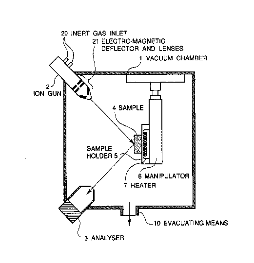
Figure 1 is a schematic view of an apparatus in accordance with the ;~-
present invention. ~ ~ ;
Figures 2A to 2C are graphs showing results of ion s~at~ering
spectroscopy in accordance with the present invention applied to surface
analysis of a YlBa2Cu30/.~ oxide superconductor thin film.
.,~ .
2~3328~ ~:
Description of the Preferred embodiments
Referring to Figure 1, there is shown a schematic view of an ion
scattering spectroscopy apparatus in accordance with the present
invention. The apparatus shown in Figure 1 comprises a v~cuum chamber
S 1 provided with an evacuating means 1~ by vvllich the vacuum chamber 1
can be evacuated to an ultra high vacuum of a pressure of lower than 1 x
10-9 Torr. The vacuum chamber 1 is also provided with an ion gun 2 on
itj one side and an analyzer 3 on its counter position. The ion gun 2 and
the analyzer can be reguL~ted in both their positions and angles. In
10 addition, the vacuum chamber 1 is provided with a sample holder 5
attached to a manipulator 6, on which a sample 4 is fastened. The
manipulator 6 has five degrees of freedom, so that it can finely move the -
sample 4 in the x, y and z directions and can finely rotate and tilt the
sample 4. The sample holder 5 comprises a heater 7 which heats the
15 sample 4.
The ion gun 2 comprises at leAst two inlets 20 through which
different inert gases are supplied, and an electro-magnetic deflector and
lenses 21. The injected inert gases are electron bombertmented in the ion
gun 2 and the ionized gases are focussed so as to fonn ion beams of small
2 0 diameters and scan by the electro-magnetic deflector and lenses 21. The
ion gun 2 is also evacuated with a differential pumping.
The analyzer 3 is a known cylindrical mirror analyzer having two
coaxial cylindrical electrodes (not shown).
According to the present invention, an ion beam of a relatively
25 small mass number inert gas accelerated by low energy irradiates the
sample 4 with a predetennined incident angle. Ions are partly scattered at
the surface of the sample 4. Energy distribution of the scattered ions is
l ~''' "' "'"'`""':'` ~.
;- 213328~
evaluated by the analyzer 3 so that only a few monolayer from the sample
surface is evaluated in its atomic composition and geometrical position of
atoms. If necessary, the analyzer 3 are changed in its position and/or
angle so as to analyze the ener~y distribution of scattered ions within the
S angle of predetermined range.
The inert gas and the acceleration energy is adjusted so that
- scattered ions from outermost monolayer of the sample surface can be
detected with releasing the sample damages as little as possible. For
example, the smal1 mass number inert gas is preferably helium and the
10 accelera~ion energy is preferably equal to or smaller than 1 keV, typically
500 eV is used. If helium ion beam of equal to or smaller than 1 keV
irradiates the sample, the sample surface can be analyzed in its
composition and geometrical position of surface atoms without damages.
Then, another ion beam of relatively large mass number inert gas
15 irradiates ~e sample 4 at a predetermined incident angle so that the
¦ outermost monolayer of the samp~e surface is peeled off and
¦ simultaneously analyzed with different resolution. It is possible to
¦ conduct only analysis of the sample surface with diffeIent resolution or to
¦ only remove the monolayer of the sample surface by controlling
¦ 2 0 acceleration energy.
¦ The inert gas and the acceleration energy is determined so that only
¦ one atomic layer of the sample surface can be precisely removed. For
¦ example, the large mass num~er inert gas is preferably neon and the
¦ acceleration energy is preferably equal to or smaller than l keV, typically
1 2 5 500 eV is used. If neon ion beam of equal to or smaller than 1 keV is
¦ irra~iates the sample, only one atomic layer of the sample surface can be
¦ peeled off. However, with precise re~ulation of acceleration energy and
I
-~ 6- ~ ~
2132~ -
ion current, it is possible to use argon ion beam having a larger mass
number.
According to the present invention, the above process is repea~ed so
that the sample is analyzed layer by layer from its outermost in its
5 composition and geometrical position.
The above analysis and peeling are prefer~bly conducted with ultra
high vacuum of a pressure of lower than 1 x 10⁻⁹ Torr. The ultra high
vacuum prevents contaminations of an exposed surface ~vith high potential
after peeling the monolayer.
10According to a preferred embodiment of the present invention,
analyzed portions of the sample surface are scanned over the range of 5 x
S square millimeters by deflecting the ion beam wi~ a small diarneter of
around 1 millimeter and the incident angle was changed by i 20 with
rotating the sample. By tllis, an extremely fine portion (both two and
15 three dimensional) of the sample surface can be analyzed so that the
surface exposed after peeling can be precisely analyzed. ~he incident ~ 1
': '$' '
angle is 37.7 and and the ion scattenng angle is 102.3" normally.
.
A surface of Y1Ba2Cu3O7 s oxide superconductor thin film was
analyzed by using the apparatus shown in Figure 1 in accordance wi~ the
2 0 present invention. It is known that YIBa2Cu3O7 ~ crystal is a secondary
crystal ha- ing a perovskite type crystal structure. The sample
Y~Ba2Cu3O7 ~ oxide superconductor thm film was an almost single crystal
thin film having a thiekness of 100 nanometers deposited on a SrTiO
(100) substrate by reactive co-evaporation method. The SrTiO3 (100)
25 substrate was fastened on the sample holder 5 and transferred into the
vacuum chamber 1 through an ultra high vacuum transportation
apparatus. The sample holder S was set on the manipulator 6.
.. ...., - s
I ~",",,.~"~"~
2133288
The vacuum chamber 1 was then isolated from the transportation
apparatus and evacuated tO 1 X 10⁻¹⁰ Torr. A helium ion beam of 500 eV
ir~adiated the sample YlBa~Cu307.g ox de superconductor thin ~llm by ~e
ion gun 2 so as to analyze a sample surface. The results are shown in
5 Figure 2A. Figure 2A is a graph showing spectra of scattered helium
ions. As shown Figure 2A, scattered ions had energy lines corresponds to
Cu and O atoms. It was clear that the most surface of the Y~Ba2Cu30
oxide superconductor thin film was covered with a Cu-O plane.
Then, a neon ion beam of 500 eV irradiated up to 10141cm2 onto the
10 sarnple YIBa2Cu307.~ oxide superconductor thin film by the ion gun 2 so
as to remove a portion of one atomic layer (Cu-O plane) of the sample
surface. A newly exposed sample surface was analyzed by irradiating
helium ion beam of 500 eV. The results are shown in Figure 2B. Figure
2B is a graph showing spectra of scattered helium ions like Figure 2A
15 As shown Figure 2B, scattered ions also had energy line corresponds tO
Cu and O atoms but with reduced intensity on Cu atoms and scattered
energy line corresponds to barium increased compared with Figure 2A.
Thereafter, a neon ion beam of 500 e~ was again irradiated with
some 1014/cm2 dose onto the sample YlBa2Cu307.~ oxide superconductor
2 0 ~in film by the ion gun 2 so as to remove the portion of one atomic layer
of the sample surface. A newly exposed sample surface was again
analyzed by irradiating helium ion beam of 500 eV. The results are
shown in Figure 2C. Figure 2C is a graph showing spectra of scattered
helium ions like Figures 2A and 2B. As shown Figure 2C, the largest
2 ~ scattered energy line was corresponds to barium. It was clear that the
second atomic layer of the Yl13a2Cu307.~ o~ide superconductor thin film
was composed of barium.
~.:
21~3288
It is known that there are three cases on Cu-O plane termination of
YlBa2Cu307 ~ oxide superconductor:
(1) Cu(l)-O ch~ins,
(2) the Cu(~)-02 plane above the Y atom along the c direction and
(3) the Cu(2)-02 plane above the Ba atom.
Inventors also confirmed that the intensity of energy line
corresponds to O atom from a surface of as-deposited YlBa2Cu307.~ oxide
superconductor thin film decreased after annealed at 500 C for 5 minutes
(T. Nakamura et al. Extended Abstr. of ISS '93, pp. 833 (1993)).
By the above analysis, it became clear that the Y~Ba2Cu307 8 oxide
superconductor thin film was terminated by Cu(l)-O chains, because Ba
atoms existed beneath and oxygen easily escaped from Cu-O chains.
During the above analysis, the pressure of the vacuum chamber was
constantly kept 1 x 10-t Torr and every process was successively
1 5 conducted.
The above process is applicable to producing a layered structure of
which a lower film was terminated at the different surface portions frorn
its nature. For example, in case of a layered structure of which a lower
film is a SrlfiO3 film, a surface of the lower film of SrTiO3 can have a
2 0 Sr-O portion and a Ti-O portion. A layered film of which an upper film
is partially deposited on the Sr-O portion of the surface of the lower film
of SrTiO3 and partially deposited on the Ti-O portion of f~he surface of
the lower film of SrTiO3 can be obtained. T~?ferefore, the characteAstics
between two films were different with these two portions because of its
2 5 schottky characteristics. In case of a layered structure of which a lower
film is a YlBa2Cu307.~ oxide ~ffuperconductor film, an upper film can be
_ _ ,............... ; ......... . - .-- - -
, ~" "~ ~"" ~ ! '"'; ~ ............. fr
~ ~'~; ~.~ ' ,i .' ~';'.~ ,~1~ ~ j~ ,.' , -~
I ~.~ .,.. ,~ ~ j. ,,j, i.. ".. ,i-~ ,.. ,~
~'' ' ?:
~ 21~238
parti~lly deposited on a Cu-O chain and on a Cu(2)-O2 plane which cause
the transportationcharacteristics difference.
As explained above, according to the present invention, there is
provided an improved ion scattering spectroscopy which can analyze a
S sample surface layer by layer and an apparatus which can conduct the
improved ion scattering spectroscopy. The improved ion scatter~ng
spectroscopy in accordance with the present invention utilizes ion beams
of inert gases having relatively small mass numbers and low energy, so
that precise analysis can be conducted without destroying the sample
10 surface. In addition, since the sample surface is removed after peeling by
an ion beam of relatively large mass number with low energy, the surface
can be removed atomic layer by atomic layer. Furthermore, the analysis
and the peeling are condllcted successively so as to prevent contamination
of a newly exposed surface having a high chemical potential so that a
15 meaningful analysis can be conducted. It is also possible to deposit an
upper film on ~e newly exposed surface having a high chemical potential
so as to fQrm a layered structure.
The invention has thus been shown and described wi~ reference to
the specific embodiments. However, it should be noted that the present
20 invention is in no way limited to the details of the illustrated structures
but changes and modifications may be made within the scope of the
appended claims.
- 10- ~ ,