Note: Descriptions are shown in the official language in which they were submitted.
2133898
INTEGRATED CIRCUITS WITH PASSIVATION AND METALLIZATION
FOR HERMETIC PROTECTION
The present invention relates to integrated
circuits which are protected from the environment. These
circuits are inexpensive to fabricate and have improved
performance and reliability.
Modern electronic circuits must be able to
withstand a wide variety of environmental conditions such as
moisture, ions, heat and abrasion. A significant amount of
work has been directed toward various protective measures to
m; n; m; ze the exposure of such circuits to the above
conditions and thereby increase their reliability and life.
Many prior art processes for protecting electronic
circuits have involved sealing or encapsulating the circuits
after they have been interconnected. For example, it is
known to use materials such as silicones, polyimides,
epoxies, other organics, plastics and the like to
encapsulate interconnected circuits. The above materials,
however, are of only limited value since most are permeable
to environmental moisture and ions.
Similarly, interconnected circuits have also been
sealed within ceramic packages. This process has proven to
be relatively effective in increasing device reliability and
is currently used in select applications. The added size,
weight and cost involved in this method, however, inhibits
widespread application in the electronic industry.
The use of`lightweight ceramic protective coatings
on electronic devices has also been suggested. For
instance, U.S. Patents 4,756,977 and 4,749,631 describe the
use of ceramic silica coatings derived from hydrogen
2133~
silsesquioxane and silicate esters, respectively, as well as
additional ceramic layers as hermetic barriers. We have
found that when such coatings are applied specifically to
integrated circuits at the wafer stage; and even though the
bond pads are subsequently opened by removing a portion of
the coating, the resultant circuits remain sealed and
exhibit increased reliability and life.
Sealing circuits at the wafer stage is also known
in the art. For example, it is known to coat fabricated
integrated circuits with ceramic materials such as silica
and/or silicon nitride by chemical vapor deposition (CVD)
techniques. These coatings are then etched back at the bond
pads for the application of leads. The wafers coated in
this manner, however, have inadequate reliability and life.
Similarly, U.S. Patent 5,136,364 teaches a method
for sealing integrated circuits at the wafer stage. The
process described therein comprises applying a first
passivation coating which overlaps the edges of an aluminum
bonding pad on an integrated circuit, applying a sequence of
conductive layers comprising a barrier metal layer and a
noble metal layer which overlay the aluminum bond pad and
which has edges which overlap the first passivation layer
and then applying a second passivation layer which overlaps
the edges of the sequence of conductive layers. This
process, however, is complex and is impractical in
conventional semiconductor fabricating facilities.
We now introduce a simple process for the
protection of integrated circuits which involves sealing the
bond pads of integrated circuits with non-corroding metal
layers and sealing the remainder of the devices with
passivation layers.
- 21~98
The present invention relates to sealed integrated
circuits. These circuits comprise a circuit subassembly
having bond pads. On the bond pads is a non-corroding metal
layer which inhibits degradation of the metal comprising the
bond pads. A passivation layer comprising 1 or more ceramic
coatings covers the surface of the subassembly and the non-
corroding metal. Openings are provided in the passivation
to expose at least a portion of the non-corroding metal for
interconnection.
The present invention is based on our finding that
integrated circuits can be sealed by the application of non-
corroding metals over the bond pads and ceramic layers over
the remainder of the circuits. The non-corroding metal
layers inhibit degradation of the bond pads and the
passivation layer inhibits degradation of the remainder of
the circuit. The resultant circuits are sealed from the
environment and can be easily interconnected by bonding
(e.g., TAB, flip-chip, wire bonding, etc. with gold, copper,
solder, etc.) to the non-corroding metal layer.
The integrated circuit subassemblies used in the
process of this invention are not critical and any which are
known in the art and/or produced commercially are useful
herein. The processes used to produce such circuits are
also known and not critical to the invention. Exemplary of
such circuits are those comprising a semiconductor substrate
(eg., silicon, gallium arsenide, etc.) having an epitaxial
layer grown thereon. This epitaxial layer is appropriately
doped to form the PN-junction regions which constitute the
active regions of the device. These active regions are
diodes and transistors which form the integrated circuit
when appropriately interconnected by a properly patterned
2133~98
metallic layer. This metallic interconnect layer terminates
at the bond pads on the exterior surface of the circuit
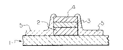
subassembly. Such circuits are represented in Figures 1 and
2 as (1) and the bond pads are represented in these Figures
as (2).
Figure 1 is a cross-sectional view of a circuit of
this invention having a diffusion barrier metal layer and
non-corroding metal layer on the bond pad and a single
ceramic coating as the passivation layer.
Figure 2 is a cross-sectional view of a circuit of
this invention having a non-corroding metal layer on the
bond pad and two ceramic coatings as the passivation layer.
In the present invention, the above integrated
circuit subassemblies are sealed by (A) applying a non-
corroding metal layer (layer 4 in Figure 2) or a barrier
metal layer and a non-corroding metal layer (layers 3 and 4,
respectively, in Figure 1) over at least a portion of the
top surfaces of the bond pads; and (B) applying a
passivation layer comprising 1 or more ceramic coatings over
the surface of this subassembly ~layers 5, 6 and 7 in
Figures 1 and 2).
The non-corroding metal layer used herein is known
in the art for use within integrated circuits for building
the multiple layers of the circuit. The material used for
this layer is not critical and can comprise any which is
stable in the environment, electrically conductive and
useful for interconnecting the circuit. Examples of such
materials include gold, copper, silver, tungsten, platinum,
solder and silver filled epoxy.
The method for applying this layer or layers is
likewise not critical. Examples of such processes include
various physical vapor deposition (PVD) techniques such as
21~3~8
sputtering and electron beam evaporation or merely
dispensing the material on the bond pad. These and other
processes are known in the art for use within integrated
circuits for building the multiple layers of the circuit and
are functional herein.
It should be noted that the materials of the bond
pad (eg., aluminum) may be incompatible with the materials
of the non-corroding metal layer (eg, gold) such that when
they are brought into contact with each other under certain
circumstances intermetallic formation ("purple plague") can
damage the circuit. To prevent such damage, it is suggested
to first apply a diffusion barrier metal layer to the bond
pads followed by application of the conductive layers as set
forth above. The diffusion barrier metal layers useful
herein are known in the art for use within integrated
circuits for building the multiple layers of the circuit.
Generally, such layers comprise metals and metal alloys such
as tungsten, titanium-tungsten and titanium nitride.
The method for forming the barrier metal layers is
not critical and many techniques are known in the art. A
common approach involves sputtering the barrier metal layer
on the surface of the circuit followed by etching.
After the bond pads have been sealed with either
the non-corroding metal layer or the barrier metal/non-
corroding metal layer, the surface of the circuit
subassembly is coated with a passivation layer. This
passivation layer generally comprises one or more ceramic
coatings.
The method for applying the passivation layer is
not critical and nearly any approach can be used.
Generally, however, the top surface of the subassembly,
including the bond pads, is entirely covered with ceramic
21~3898
coating(s) and then the coating(s) covering the bond pads is
etched to allow interconnection of the circuit. One example
of a method for depositing these coatings involves applying
a silicon-containing ceramic material by a process
comprising coating the circuit with a composition comprising
a preceramic silicon-containing material followed by
converting the preceramic silicon-containing material to a
ceramic. Typically, the preceramic silicon-containing
material is converted to a ceramic by heating it to a
sufficient temperature. This approach is particularly
advantageous in that the resultant coating is planar in
addition to being hermetic.
As used herein, the term "preceramic silicon-
containing material" describes material which can be
rendered sufficiently flowable to impregnate and coat the
surface of a circuit and which can be subsequently converted
to a solid layer exhibiting properties generally recognized
by those skilled in the art as characteristic of a ceramic.
These materials include precursors to silicon oxides,
silicon nitride, silicon oxynitride, silicon oxycarbide,
silicon carbonitride, silicon oxycarbonitride and silicon
carbide.
The preferred preceramic silicon-containing
materials to be used in the process of this invention are
precursors to silicon oxides, especially silica. The
silica precursors which may be used are hydrogen
silsesquioxane resin (H-resin), hydrolyzed or partially
hydrolyzed RnSi(OR~4_n, or combinations of the above, in
which each R is independently an aliphatic, alicyclic or
aromatic substituent of 1-20 carbon atoms, preferably 1-4,
such as an alkyl (e.g., methyl, ethyl and propyl), alkenyl
(e.g., vinyl or allyl), alkynyl (e.g., ethynyl),
2133~g8
cyclopentyl, cyclohexyl and phenyl and n is 0-3, preferably
0 or 1.
H-resin is used in this invention to describe a
variety of hydridosilane resins having units of the
structure HSi(oH)x(oR)yOz/2 in which each R is independently
an organic group which, when bonded to silicon through the
oxygen atom, forms a hydrolyzable substituent, x = 0-2, y =
0-2, z = 1-3 and x + y + z = 3. These resins may be either
fully condensed (x = 0, y = 0 and z = 3) or they may be only
partially hydrolyzed (y does not equal 0 over all the units
of the polymer) and/or partially condensed (x does not equal
0 over all the units of the polymer). Although not
represented by this structure, various units of these resins
may have either zero or more than one Si-H bond due to
various factors involved in their formation and handling.
Exemplary of substantially condensed H-resins (less than 300
ppm silanol) are those formed by the process of U.S. Patent
3,615,272. This polymeric material has units of the formula
(HSiO3/2)n in which n is generally 8-1000. The preferred
resin has a number average molecular weight of from 800-2900
and a weight average molecular weight of between 8000-28,000
(obtained by GPC analysis using polydimethylsiloxane as a
calibration standard). When heated sufficiently, this
material yields a ceramic coating essentially free of SiH
bonds.
Exemplary H-resin which may not be fully condensed
include those of U.S. Patent 5,010,159 or those of U.S.
Patent 4,999,397. Exemplary H-resin which is not fully
hydrolyzed or condensed is that formed by a process which
comprises hydrolyzing a hydrocarbonoxy hydridosilane with
water in an acidified oxygen-containing polar organic
solvent.
21338~8
A platinum, rhodium or copper catalyst may be
admixed with the hydrogen silsesquioxane to increase the
rate and extent of its conversion to silica. Any platinum,
rhodium or copper compound or complex that can be
solubilized in this solution will be operable. For
instance, an organoplatinum composition such as platinum
acetylace tonate or rhodium catalyst RhCl3[S(CH2CH2CH2CH3) 2 ] 3,
obtained from Dow Corning Corporation, Midland, Michigan is
suitable. The above catalysts are generally added to the
solution in an amount of between 5 and 500 ppm platinum or
rhodium based on the weight of resin.
The second type of silica precursor material
useful herein includes hydrolyzed or partially hydrolyzed
compounds of the formula RnSi(OR)4_n in which R and n are as
defined above. Some of these materials are commercially
available, for example, under the tradename ACCUGLASS
(Allied Signal). Specific compounds of this type include
methyltriethoxysilane, phenyltriethoxysilane,
diethyldiethoxysilane, methyltri-methoxysilane,
dimethyldimethoxysilane, phenyltri-methoxysilane,
vinyltrimethoxysilane, tetramethoxysilane,
tetraethoxysilane, tetrapropoxysilane and tetrabutoxysilane.
After hydrolysis or partial hydrolysis of these compounds,
the silicon atoms therein may be bonded to C, OH or OR
groups, but a substantial portion of the material is
believed to be condensed in the form of soluble Si-O-Si
resins. Compounds in which x = 2 or 3 are generally not
used alone as volatile cyclic structures are generated
during pyrolysis, but small amounts of said compounds may be
cohydrolyzed with other silanes to prepare useful preceramic
materials.
2133~98
In addition to the above SiO2 precursors, other
ceramic oxide precursors may also be advantageously used
herein either solely or in combination with the above SiO2
precursors. These precursors include compounds of various
metals such as aluminum, titanium, zirconium, tantalum,
niobium and/or vanadium, as well as various non-metallic
compounds such as those of boron or phosphorous which may be
dissolved in solution, hydrolyzed and subsequently pyrolyzed
at relatively low temperatures to form ceramic oxides.
The above ceramic oxide precursor compounds
generally have one or more hydrolyzable groups bonded to the
above metal or non-metal, depending on the valence of the
metal. The number of hydrolyzable groups to be included in
these compounds is not critical as long as the compound is
soluble in the solvent. Likewise, selection of the exact
hydrolyzable substituent is not critical since the
substituents are either hydrolyzed or pyrolyzed out of the
system. Typical hydrolyzable groups include alkoxy, such as
methoxy, propoxy, butoxy and hexoxy; acyloxy, such as
acetoxy; and other organic groups bonded to said metal or
non-metal through an oxygen such as acetylacetonate or an
amino groups. Specific compounds include zirconium
tetracetylacetonate, titanium dibutoxy diacetylacetonate,
aluminum triacetyl-acetonate, tetraisobutoxy titanium and
Ti(N(CH3)2)4-
When SiO2 is to be combined with one of the above
ceramic oxide precursors, generally it is used in an amount
such that the final ceramic contains 70 to 99.9 percent by
weight SiO2.
Examples of other silicon-containing preceramic
materials include silicon carbonitride precursors such as
hydridopolysilazane (HPZ) resin and methylpolydisilylazane
~38g~
(MPDZ) resin. Processes for the production of these
materials are described in U.S. Patents 4,540,803 and
4,340,619, respectively. Examples of silicon carbide
precursors include polycarbosilanes and examples of silicon
nitride precursors include polysilazanes. Oxygen can be
incorporated into the ceramics resulting from the above
precursors or the precursors can be converted to silica by
pyrolyzing them in an oxygen-containing environment.
The above silicon-containing preceramic material
is then used to coat the integrated circuit. The material
can be used in any practical form but it is preferred to use
a liquid comprising the preceramic material in a suitable
solvent. If this solution approach is used, the preceramic
liquid is generally formed by simply dissolving or
suspending the preceramic material in a solvent or mixture
of solvents. Various facilitating measures such as stirring
and/or heat may be used to assist in the
dissolution/dispersion. The solvents which may be used in
this method include alcohols such as ethyl or isopropyl;
aromatic hydrocarbons such as benzene or toluene; alkanes
such as n-heptane or dodecane; ketones; cyclic
dimethylpolysiloxanes; esters or glycol ethers; in an amount
sufficient to dissolve or disperse the above materials to
low solids. For instance, enough of the above solvent can
be included to form a 0.1-85 weight percent solution.
The circuit is then coated with this liquid by
means such as spin, spray, dip or flow coating and the
solvent is allowed to evaporate. Any suitable means of
evaporation such as simple air drying by exposure to an
ambient environment or the application of a vacuum may be
used.
21~38g8
Although the above described methods primarily
focus on using a solution approach, one skilled in the art
would recognize that other equivalent means (eg., melt
impregnation) would also function herein and are
contemplated by this invention.
The preceramic material is then typically
converted to the silicon-containing ceramic by heating it to
a sufficient temperature. Generally, the temperature is in
the range of 50 to 1000C. depending on the pyrolysis
atmosphere and the preceramic compound. Preferred
temperatures are in the range of 50 to 600C. and more
preferably 50-400C. Heating is generally conducted for a
time sufficient to ceramify, generally up to about 6 hours,
with less than 2 hours being preferred.
The above heating may be conducted at any
effective atmospheric pressure from vacuum to
superatmospheric and under any effective oxidizing or non-
oxidizing gaseous environment such as those comprising air,
2~ an inert gas (N2, etc.), ammonia, amines, moisture and
N20 .
Any method of heating such as the use of a
convection oven, rapid thermal processing, hot plate or
radiant or microwave energy is generally functional herein.
The rate of heating, moreover, is also not critical, but it
is most practical and preferred to heat as rapidly as
possible.
Additional examples of methods for the application
of the passivation include PVD or CVD of coatings such as
silicon oxygen containing coatings, silicon containing
coatings, silicon carbon containing coatings, silicon
nitrogen containing coatings, silicon oxygen nitrogen
coatings, silicon nitrogen carbon containing coatings,
2133~g8
silicon oxygen carbon containing coatings, silicon oxygen
carbon nitrogen containing coatings and/or diamond like
carbon coatings.
The materials and methods for the formation of
these ceramic coatings are not critical to the invention and
many are known in the art. Examples of applicable methods
include a variety of CVD techniques such as conventional
CVD; photochemical vapor deposition; plasma enhanced CVD
(PECVD), electron cyclotron resonance (ECR), jet vapor
deposition and a variety of PVD techniques such as
sputtering, electron beam evaporation and the like. These
processes involve either the addition of energy (in the form
of heat or plasma) to a vaporized species to cause the
desired reaction or the focusing of energy on a solid sample
of the material to cause its deposition.
In conventional CVD, the coating is deposited by
passing a stream of the desired precursor gases over a
heated substrate. When the precursor gases contact the hot
surface, they react and deposit the coating. Substrate
temperatures in the range of 100-1000C. are sufficient to
form these coatings in several minutes to several hours,
depending on the precursors and the thickness of the coating
desired. If desired, reactive metals can be used in such a
process to facilitate deposition.
In PECVD, the desired precursor gases are reacted
by passing them through a plasma field. The reactive
species thereby formed are then focused at the substrate and
readily adhere. Generally, the advantage of this process
over CVD is that lower substrate temperature can be used.
For instance, substrate temperatures of 20 to 600C. are
functional.
21338g8
The plasma used in such processes can comprise
energy derived from a variety of sources such as electric
discharges, electromagnetic fields in the radio-frequency or
microwave range, lasers or particle beams. Generally
preferred in most plasma deposition processes is the use of
radio frequency (10 kHz-102 MHz) or microwave ~0.1-10 GHz)
energy at moderate power densities (0.1-5 watts/cm2). The
specific frequency, power and pressure, however, are
generally tailored to the precursor gases and the equipment
used.
Examples of suitable processes for the deposition
of the silicon containing coating described above include
(a) the CVD of a silane, halosilane, halodisilane,
halopolysilane or mixtures thereof, (b) the PECVD of a
silane, halosilane, halodisilane, halopolysilane or mixtures
thereof or (c) the metal assisted chemical vapor deposition
(MACVD) of a silane, halosilane, halodisilane,
halopolysilane or mixtures thereof.
Examples of suitable processes for the deposition
of the silicon carbon containing coating described above
include (1) the CVD of a silane, alkylsilane, halosilane,
halodisilane, halopolysilane or mixtures thereof optionally
in the presence of an alkane of one to six carbon atoms or
an alkyl-silane, (2) the PECVD of a silane, alkylsilane,
halosilane, halodisilane, halopolysilane or mixtures thereof
optionally in the presence of an alkane of one to six carbon
atoms or an alkylsilane or (3) the PECVD of a
silacyclobutane or disilacyclobutane as described in U.S.
Patent 5,011,706.
Examples of suitable processes for the deposition
of the silicon oxygen carbon containing coating described
above include (1) the CVD of a silane, alkylsilane,
- 2~33~98
14
halosilane, halodisilane, halopolysilane or mixtures thereof
optionally in the presence of an alkane of one to six carbon
atoms or an alkylsilane and further in the presence of an
oxidizing gas such as air, oxygen, ozone, nitrous oxide and
the like, (2) the PECVD of a silane, alkylsilane,
halosilane, halodisilane, halopolysilane or mixtures thereof
optionally in the presence of an alkane of one to six carbon
atoms or an alkylsilane and further in the presence of an
oxidizing gas such as air, oxygen, ozone, nitrous oxide and
the like or (3) the PECVD of a silacyclobutane or
disilacyclobutane as described in U.S. Patent 5,011,706, in
the presence of an oxidizing gas such as air, oxygen, ozone,
nitrous oxide and the like.
Examples of suitable processes for the deposition
of the silicon nitrogen containing coating described above
include (A) the CVD of a silane, halosilane, halodisilane,
halopolysilane or mixtures thereof in the presence of
ammonia, (B) the PECVD of a silane, halosilane,
halodisilane, halopolysilane or mixtures thereof in the
presence of ammonia, (C) the PECVD of a SiH4 - N2 mixture
such as that described by Ionic Systems or that of Katoh in
the Japanese Journal of Applied Physics, vol. 22, #5, pp.
1321-1323 or (D) reactive sputtering such as that described
in Semiconductor International, p 34, August 1987.
Examples of suitable processes for the deposition
of the silicon oxygen nitrogen containing coating described
above include (A) the CVD of a silane, halosilane,
halodisilane, halopolysilane or mixtures thereof in the
presence of ammonia and an oxidizing gas such as air,
oxygen, ozone, nitrous oxide and the like, (B) the PECVD of
a silane, halosilane, halodisilane, halopolysilane or
2133~
mixtures thereof in the presence of ammonia and an oxidizing
gas such as air, oxygen, ozone, nitrous oxide and the like,
(C) the PECVD of a SiH4 - N2 mixture such as that described
by Ionic Systems or that of Katoh in the Japanese Journal of
Applied Physics, vol. 22, #5, pp. 1321-1323 in the presence
of an oxidizing gas such as air, oxygen, ozone, nitrous
oxide and the like or (D) reactive sputtering such as that
described in Semiconductor International, p 34, August 1987
in the presence of an oxidizing gas such as air, oxygen,
ozone, nitrous oxide and the like.
Examples of suitable processes for the deposition
of the silicon oxygen containing coating described above
include (A) the CVD of a silane, halosilane, halodisilane,
halopolysilane or mixtures thereof in the presence of an
oxidizing gas such as air, oxygen, ozone, nitrous oxide and
the like, (B) the PECVD of a silane, halosilane,
halodisilane, halopolysilane or mixtures thereof in the
presence of an oxidizing gas such as air, oxygen, ozone,
nitrous oxide and the like, (c) the CVD or PECVD of
tetraethylorthosilicate, methyltrimethoxysilane,
methylhydrogensiloxanes, dimethylsiloxanes and the like in
the presence of an oxidizing gas such as air, oxygen, ozone,
nitrous oxide and the like or (d) the CVD or PECVD of
hydrogen silsesquioxane resin in the presence of an
oxidizing gas such as air, oxygen, ozone, nitrous oxide and
the like as described in U.S. Patent 5,165,955.
Examples of suitable processes for the deposition
of the silicon carbon nitrogen containing coating described
above include (i) the CVD of hexamethyldisilazane, (ii) the
PECVD of hexamethyldisilazane, (iii) the CVD of silane,
alkylsilane, halosilane, halodisilane, halopolysilane or
mixture thereof optionally in the presence of an alkane of
2133~98
16
one to six carbon atoms or an alkylsilane and further in the
presence of ammonia or (iv) the PECVD of a silane,
alkylsilane, halosilane, halodisilane, halopolysilane or
mixture thereof optionally in the presence of an alkane of
one to six carbon atoms or an alkylsilane and further in the
presence of ammonia.
Examples of suitable processes for the deposition
of the silicon oxygen carbon nitrogen containing coating
described above include (i) the CVD of hexamethyldisilazane
in the presence of an oxidizing gas such as air, oxygen,
ozone, nitrous oxide and the like, ~ii) the PECVD of
hexamethyldisilazane in the presence of an oxidizing gas
such as air, oxygen, ozone, nitrous oxide and the like,
(iii) the CVD of silane, alkylsilane, halosilane,
halodisilane, halopolysilane or mixture thereof optionally
in the presence of an alkane of one to six carbon atoms or
an alkylsilane and further in the presence of ammonia and an
oxidizing gas such as air, oxygen, ozone, nitrous oxide and
the like or (iv) the PECVD of a silane, alkylsilane,
halosilane, halodisilane, halopolysilane or mixture thereof
optionally in the presence of an alkane of one to six carbon
atoms or an alkylsilane and further in the presence of
ammonia and an oxidizing gas such as air, oxygen, ozone,
nitrous oxide and the like.
Examples of suitable processes for the deposition
of the diamond-like carbon coating described above include
exposing the substrate to an argon beam containing a
hydrocarbon in the manner described in NASA Tech Briefs,
November 1989 or by one of the methods described by Spear in
J. Am. Ceram. Soc., 72, pp. 171-191 (1989).
It should be noted that the passivation may be
doped with other agents, if desired. For instance, the
98
17
coatings may be doped with boron, phosphorous or carbon to
modify its characteristics.
Either one or more of the above coatings may be
used as the passivation. In a preferred embodiment of the
invention, a silicon-containing ceramic layer derived from a
preceramic silicon-containing material is used as a first
planar layer and a second layer of a material such as
silicon nitride or silicon carbide is applied on top of the
first layer by CVD.
After the passivation has been applied, the
coating covering the bond pad metallization is etched or
partially etched to expose the top surface of the non-
corroding metal layer to allow for interconnection of the
circuit. In one embodiment of the invention, the
passivation on the entire top surface of the bond pad can be
removed. In the preferred embodiment, however, only a
portion of the passivation on the top surface of bond pad is
removed such that the passivation overlaps the edges and the
top surface of the bond pad. It should be noted, however,
that other approaches which result in open bond pads may
also be used (eg., depositing the coating only around the
bond pads).
The method of etching is not critical and nearly
any process known in the art will function herein. This
includes dry etching (eg., with plasma), wet etching (eg.,
with aqueous hydrofluoric acid) and/or laser ablation.
The resultant circuits are hermetically sealed
such that they can be handled and/or transported without
damage. In addition, either of the passivation layers may
absorb W or visible light or contain pigments or fillers
which absorb W or visible light to prevent damage and
inhibit inspection.
213~898
After interconnection, the device can also be
packaged by conventional techniques known in the art. For
instance, the device can be embedded within an organic
encapsulant such as a polyimide, an epoxy or PARYLENETM; it
can be embedded within a silicone encapsulant; it can be
included in a plastic package for additional protection; or
it can be contained in a module or assembly without any
further primary packaging.