Note: Descriptions are shown in the official language in which they were submitted.
21~4~'~6
PATENT APPLICATION
Attorney's Docket No. D/92281
LONG LIFE PHOTORECEPTOR
BACKGROUND OF THE INVENTION
This invention relates in general to electrophotographic imaging
members and, more specifically, to layered photoreceptor structures with
overcoatings containing hydrogen bonded materials and processes for
making and using the photoreceptors.
Electrophotographic imaging members, i.e. photoreceptors,
typically include a photoconductive layer formed on an electrically
conductive substrate. The photoconductive layer is an insulator in the dark
so that electric charges are retained on its surface. Upon exposure to light,
the charge is dissipated.
A latent image is formed on the photoreceptor by first uniformly
depositing an electric charge over the surface of the photoconductive layer
by one of any suitable means well known in the art. The photoconductive
layer functions as a charge storage capacitor with charge on its free surface
and an equal charge of opposite polarity (the counter charge) on the
conductive substrate. A light image is then projected onto the
photoconductive layer. On those portions of the photoconductive layer
that are exposed to light, the electric charge is conducted through the layer
reducing the surface charge. The portions of the surface of the
photoconductor not exposed to light retain their surface charge. The
quantity of electric charge at any particular area of the photoconductive
surface is inversely related to the illumination incident thereon, thus
forming an electrostatic latent image.
The photodischarge of the photoconductive layer requires that
the layer photogenerate conductive charge and transport this charge
through the layer thereby neutralizing the charge on the surface. Two
types of photoreceptor structures have been employed: multilayer
structures wherein separate layers perform the functions of charge
generation and charge transport, respectively, and single layer
21~42~,6
photoconductors which perform both functions. These layers are formed on an
electrically conductive substrate and may include an optional charge blocking
and an adhesive layer between the conductive layer and the photoconducting
layer or layers. Additionally, the substrate may comprise a non-conducting
mechanical support with a conductive surface. Other layers for providing
special functions such as incoherent reflection of laser light, dot patterns
for
pictorial imaging or subbing layers to provide chemical sealing and/or a
smooth
coating surface may be optionally be employed.
One common type of photoreceptor is a multilayered device that
comprises a conductive layer, a blocking layer, an adhesive layer, a charge
generating layer, and a charge transport layer. The charge transport layer can
contain an active aromatic diamine molecule, which enables charge transport,
dissolved or molecularly dispersed in a film forming binder. This type of
charge
transport layer is described, for example in US-A, 4,265,990. Other charge
transport molecules disclosed in the prior art include a variety of electron
donor,
aromatic amines, oxadiazoles, oxazoles, hydrazones and stilbenes for hole
transport and electron acceptor molecules for electron transport. Another type
of
charge transport layer has been developed which utilizes a charge transporting
polymer wherein the charge transporting moiety is incorporated in the polymer
as a group pendant from the backbone of the polymer backbone or as a moiety
in the backbone of the polymer. These types of charge transport polymers
include materials such as poly(N-vinylcarbazole), polysilylenes, and others
including those described, for example, in US-A 4,618,551, 4,806,443,
4,935,487, and 4,956,440. Other charge transporting materials include
polymeric arylamine compounds and related polymers described in US-A
4,801,517, US-A 4,806,444, US-A 4,818,650, US-A 4,806,443 and US-A
5,030,532.
r. 2 r,
5~~~,,.'. °i,
~Y:rl
21342T6
One of the design criteria for the selection of the photosensitive
pigment for a charge generator layer and the charge transporting molecule
or polymer for a transport layer is that, when light photons photogenerate
holes in the pigment, the holes be efficiently injected into the charge
transporting moiety in the transport layer. More specifically, the injection
efficiency from the pigment to the transport layer should be high. A
second design criterion is that the injected holes be transported across the
charge transport layer in a short time; shorter than the time duration
between the exposure and development stations in an imaging device. The
transit time across the transport layer is determined by the charge carrier
mobility in the transport layer. The charge carrier mobility is the velocity
per unit field and has dimensions of cm2/volt sec. The charge carrier
mobility is a function of the structure of the charge transporting moiety,
the concentration of the charge transporting moiety in the transport layer
and the electrically "inactive" binder polymer in which the charge transport
molecule is dispersed ( if the transport layer consists of charge transporting
molecules dispersed in a binder). It is believed that the injection efficiency
can be maximized by choosing a transporting moiety whose ionization
potential is lower than that of the pigment (assuming the charge
transporting carriers are holes). However, low ionization potential
molecules may have other deficiencies, one of which is their instability in an
atmosphere of corona effluents. A copy quality defect resulting from the
chemical interaction of the surface of the transport layer with corona
effluents is referred to as "parking deletion" and is described in detail
below.
Photoreceptors are cycled many thousands of times in automatic
copiers, duplicators and printers. This cycling causes degradation of the
imaging properties of photoreceptors, particularly multilayered organic
3
B
~1 ~ 42'6
photoconductors which utilize organic film forming polymers and small
molecule low ionization donor material in the charge transport layers.
Such wear is accelerated when the photoreceptor is utilized in systems
employing abrasive development systems such as single component
development systems. Wear is an even greater problem where a drum is
utilized which has such a small diameter that it must rotate many, many
times merely to form images for each conventional size 8.5 inch by 11 inch
document. Wear of the photoreceptor can be compensated by increasing
the thickness of the charge transport layer. However, large increases in
thickness of the charge transport layer can render the photoreceptor
inoperable at high imaging process speeds because of the inadequate (very
long) transit times of common charge transport layer materials. Also, large
decreases in thickness due to wear can cause dramatic changes in electrical
characteristics in only a few thousand cycles that cannot be readily
compensated by even sophisticated computerized control apparatus.
When the electrophotographic imaging member is utilized in
liquid ink development systems, leaching of small molecules from the
charge transport layer into the liquid development can occur. Loss of the
small molecule material due to leaching causes undesirable deterioration in
electrical properties of the photoreceptor. Also, undesirable crystallization
of the small molecule in the charge transport layer can adversely affect the
electrical imaging characteristics of the photoreceptor.
Reprographic machines utilizing multilayered organic
photoconductors also employ corotrons or scorotrons to charge the
photoconductors prior to imagewise exposure. During the operating
lifetime of these photoconductors they are subjected to corona effluents
which include ozone, various oxides of nitrogen, etc. It is believed that
some of these oxides of nitrogen are converted to nitric acid in the presence
of water molecules present in the ambient operating atmosphere. The top
surface of the photoconductor is exposed to the nitric acid during
operation of the machine and charge transporting moiety at the very top
surface of the transport layer are converted to what is believed to be the
nitrated species of the molecules and these could form an electrically
-4-
~~~~2~6
conductive film. However, during operation of the machine, the cleaning
subsystem continuously removes (by wear) a region of the top surface
thereby preventing accumulation of the conductive species. Unfortunately,
such is not the case when the machine is not operating (i.e. in idle mode)
between two large copy runs. During the idle mode between long copy
runs, a specific segment of the photoreceptor comes to rest (is parked)
beneath a corotron that had been in operation during the long copy run.
Although the high voltage to the corotron is turned off during the time
period when the photoreceptor is parked, some effluents (e.g. nitric acid,
etc.) continue to be emitted from the corotron shield, corotron housing,
etc. This effluent emission is concentrated in the region of the stationary
photoreceptor parked directly underneath the corotron. The effluents
render that surface region electrically conductive. When machine
operation is resumed for the next copy run, image spreading and loss of
resolution occurs in the region of the photoconductor where surface
conductivity has increased. Deletion may also be observed in the loss of
fine lines and details in the final print. Thus, the corona induced changes
primarily occur at the surface region of the charge transport layer. These
changes are manifested in the form of increased conductivity which results
in loss of resolution of the final toner images. Loss of resolution along the
entire imaging surface can occur due to an increase in surface conductance
caused by corona species interaction. In the case of excessive increases in
conductivity, there can be regions of extreme deletions in the images. This
problem is particularly severe in devices employing arylamine charge
transport molecules such as N,N'-Biphenyl-N,N'-bis(3-methylphenyl)-(1,1'-
biphenyl)-4,4'-diamine and charge transport polymers incorporating
diamine transporting moiety.
Although, "parking deletion" is described above, in some cases
deletion might occur in all portions of the photoconductor. This will
depend on the number and type of corotrons employed, the design of the
photoconductor cavity and air-flow patterns around the photoconductor.
Thus, although the charge transport moiety meets most other
electrophotographic criteria such as being devoid of traps, having high
-5-
z~~~~~s
injection efficiency from many pigments, ease in synthesizing, and
inexpensive, it encounters serious parking and other deletion problems.
INFORMATION DISCLOSURE STATEMENT
US-A 4,297,425 to Pai et al., issued October 27, 1981 - A layered
photosensitive member is disclosed comprising a generator layer and a
transport layer containing a combination of diamine and triphenyl
methane molecules dispersed in a polymeric binder.
US-A 4,050,935 to Limburg et al., issued September 27, 1977 - A
layered photosensitive member is disclosed comprising a generator layer of
trigonal selenium and a transport layer of bis(4-diethylamino-2-
methylphenyl)phenylmethane molecularly dispersed in a polymeric binder.
US-A 4,457,994 to Pai et al. et al, issued Juiy 3 1984 - A layered
photosensitive member is disclosed comprising a generator layer and a
transport layer containing a diamine type molecule dispersed in a polymeric
binder and an overcoat containing triphenyl methane molecules dispersed
in a polymeric binder.
US-A 4,281,054 to Horgan et al., issued July 28, 1981 - An
imaging member is disclosed comprising a substrate, an injecting contact,
or hole injecting electrode overlying the substrate, a charge transport layer
comprising an electrically inactive resin containing a dispersed electrically
active material, a layer of charge generator material and a layer of
insulating organic resin overlying the charge generating material. The
charge transport layer can contain triphenylmethane.
US-A 4,871,634 to Limburg et al., issued October 3, 1989 - An
electrostatographic imaging member is disclosed which contains at least
one electrophotoconductive layer, the imaging member comprising a
photogenerating material and a hydroxy arylamine compound represented
by a certain formula. The hydroxy arylamine compound can be used in an
overcoating with the hydroxy arylamine compound bonded to a resin
capable of hydrogen bonding such as a polyamide possessing alcohol
solubility.
-6-
z~ 3 42~s
US-A 4,515,882 to Mammino et al, issued May 7, 1985 - An
electrophotographic imaging system is disclosed which utilizes a member
comprising at least one photoconductive layer and an overcoating layer
comprising a film forming continuous phase comprising charge transport
molecules and finely divided charge injection enabling particles dispersed
in the continuous phase, the insulating overcoating layer being
substantially transparent to activating radiation to which the
photoconductive layer is sensitive and substantially electrically insulating
at
low electrical fields.
US-A 4,599,286 to Limburg et al., issued Juiy 8, 1982 - An
electrophotographic imaging member is disclosed comprising a charge
generation layer and a charge transport layer, the transport layer
comprising an aromatic amine charge transport molecule in a continuous
polymeric binder phase and a chemical stabilizer selected from the group
consisting of certain nitrone, isobenzofuran, hydroxyaromatic compounds
and mixtures thereof. An electrophotographic imaging process using this
member is also described.
An electrophotographic imaging member has been previously
disclosed comprising a substrate, a charge generating layer, a charge
transport layer comprising charge transporting molecules dispersed in a first
polymer binder, and an overcoat layer comprising a triphenyl methane
molecule dispersed in a second polymer binder, the second polymer binder
being soluble in a solvent in which the first polymer binder is insoluble. The
overcoat layer may contain an optional charge transport molecule. The
device may also include any suitable optional charge blocking, adhesive and
other sub layers. This electrophotographic imaging member is fabricated by
forming on a charge generating layer a first coating comprising charge
transporting molecules dispersed in a solution of a first polymer binder
dissolved in a first solvent, drying the coating to remove the solvent to form
a
substantially dry charge transport layer, forming on the charge transport
layer
a second coating comprising
21342'6
triphenyl methane molecules and charge transporting molecules dispersed
in a solution of a second polymer binder dissolved in a second solvent, the
first polymer binder being insoluble in the second solvent, and drying the
second coating to remove the second solvent to form a substantially dry
overcoat layer. This electrophotographic imaging member may be utilized in
an electrophotographic imaging process.
An electrophotographic imaging member has been previously
disclosed which comprises a substrate, a charge generating layer, a charge
transport layer, and an overcoat layer comprising a small molecule hole
transporting arylamine having at least two hydroxy functional groups, a
hydroxy or multihydroxy triphenyl methane and a polyamide film forming
binder capable of forming hydrogen bonds with the hydroxy functional groups
the hydroxy arylamine and hydroxy or multihydroxy triphenyl methane. This
overcoat layer may be fabricated using an alcohol solvent. This
electrophotographic imaging member may be utilized in an
electrophotographic imaging process.
Also disclosed is an electrophotographic imaging member
comprising a substrate, a charge generating layer, a charge transport layer,
and an overcoat layer comprising a small molecule hole transporting
arylamine having at least two hydroxy functional groups, a hydroxy terminated
dimethyl siloxane and a polyamide film forming binder capable of forming
hydrogen bonds with the hydroxy functional groups on the hydroxy arylamine
and hydroxy diorgano siloxane. This overcoat layer may be fabricated using
an alcohol solvent. This electrophotographic imaging member may be utilized
in an electrophotographic imaging process.
g
B
2134276
Although acceptable images may be obtained when chemical
triphenyl urethanes are incorporated within the bulk of the charge
transport layers, the photoreceptor can exhibit at least two deficiencies
when subjected to extensive cycling. One is that the presence of the
triphenyl methane in the bulk of the charge transport layer results in
trapping of photoinjected holes from the generator layer into the transport
layer giving rise to higher residual potentials. This can cause a condition
known as cycle-up in which the residual potential continues to increase
with multi-cycle operation. This can give rise to increased densities in the
background areas of the final images. A second undesirable effect due to
the addition of the triphenyl methane in the bulk of the transport layer is
that some of these molecules migrate into the generator layer during the
process of the fabrication of the transport layer. The presence of these
molecules on the surface of the pigment in the generator layer could result
in cyclic instabilities, particularly in long image cycling runs. These two
deficiencies limits the concentration of the triphenyl urethanes that can be
added in the transport layer.
Where photoreceptors are overcoated with films containing
triphenyl urethanes, intermixing of the overcoat and the transport layers
occur which can render the overcoat very ineffective. This intermixing leads
to the incorporation of hydroxy triphenyl urethanes in the bulk of the
transport layer causing cycle-up. Also, the intermixing causes a reduction of
the concentration of triphenyl urethanes on the outer surface of the
photoreceptor. The concentration of triphenyl urethanes in the outer
surface region of the photoreceptor prevents the aforementioned deletion.
Thus, there is a continuing need for photoreceptors having
improved resistance to corona effluent induced deletions without
increased densities in the background areas of the final images, migration
of additives into the generator layer during fabrication of the transport
layer, and cyclic instabilities.
_g_
B
w. 213476
SUMMARY OF THE INVENTION
It is, therefore, an object of an aspect of the present invention to provide
an improved electrophotographic imaging member which overcomes the above-
noted deficiencies.
It is an object of an aspect of the present invention to provide an
improved electrophotographic imaging member exhibiting greater resistance to
abrasion during image cycling.
It is an object of an aspect of the present invention to provide an
improved electrophotographic imaging member that resists leaching of
1 o components from the charge transport layer during liquid development.
It is an object of an aspect of the present invention to provide an
improved electrophotographic imaging member that resists cracking of the
charge transport layer during liquid development.
It is an object of an aspect of the present invention to provide an
improved electrophotographic imaging member which reduces crystallization of
small molecules in the charge transport layer.
It is an object of an aspect of the present invention to provide an
improved electrophotographic imaging member which is stable against copy
defects such as print deletion.
2 o It is an object of an aspect of the present invention to provide an
improved electrophotographic imaging member having greater stability against
corona induced chemical changes.
It is an object of an aspect of the present invention to provide an
improved electrophotographic imaging member which avoids residual charge
2 5 build up.
It is an object of an aspect of the present invention to provide an
improved electrophotographic imaging member which is mechanically stronger.
It is an object of an aspect of the present invention to provide an
improved electrophotographic imaging member having an overcoating free of
3 o phase separation of component materials.
The foregoing objects and others are accomplished in accordance with
this invention by providing an electrophotographic
A
213427fi
imaging member comprising a substrate, a charge generating layer, a
charge transport layer, and an overcoat layer comprising a small molecule
hole transporting triphenyl methane having at least one hydroxy functional
group, and a polyamide film forming binder capable of forming hydrogen
bonds with the hydroxy functional groups of the hydroxy triphenyl
methane. This overcoat layer may be fabricated using an alcohol solvent.
This electrophotographic imaging member may be utilized in an
electrophotographic imaging process.
Other aspects of this invention are as follows:
An electrophotoraphic imaging member comprising, in order, a
substrate, a charge generating layer, a charge transport layer, and an
overcoat layer
compriing a hydroxy triphenyl methane having at least one hydroxy functional
group
and a polyamide film forming binder capable of forming hydrogen bonds with
said at
least one hydroxy functional group of said hydroxy triphenyl methane molecule,
said
charge transport layer comprising less than about two percent of said hydroxy
triphenyl methane molecules based on the weight of said charge transport
layer.
A process for fabricating an electrophotographic imaging member
comprising providing a substrate coated with a charge generating layer and a
charge
transport layer comprising charge transporting molecules dispersed in a
solution of an
alcohol insoluble polymer binder or a charge transporting polymer which is
insoluble
in alcohol, forming on said charge transport layer a coating of a solution
consisting
essentially of a hydroxy triphenyl methane compound having at least one
hydroxy
functional group and a polyamide film forming binder capable of forming
hydrogen
bonds with said hydroxy functional groups of said hydroxy triphenyl methane
compound dissolved in an alcohol solvent, and drying said coating to remove
said
alcohol solvent to form a dry overcoat layer consisting essentially of said
hydroxy
triphenyl methane compound and said polyamide film forming binder, said charge
transport layer comprising less than about two percent of said hydroxy
triphenyl
methane molecules based on the weight of said charge transport layer.
.~ a
21342'6
An electrophotographic imaging member comprising a substrate, a
charge generating layer, a charge transport layer, and an overcoat layer
comprising
bis-(4-(beta-hydroxyethyl ethylamino)-2-methylphenyl)-phenylmethane having
hydroxy functional groups and a polyamide film forming binder capable of
forming
hydrogen bonds with said hydroxy functional groups, said charge transport
layer
comprising less than about two percent of said hydroxy triphenyl methane
molecules
based on the weight of said charge transport layer.
BRIEF DESCRIPTION OF THE DRAWINGS
FIG. 1 illustrates a structural formula of an aromatic diamine
molecule.
F1G. 2 illustrates a structural formula of a polycarbonate binder
segment.
FIG. 3 illustrates electron transfer from a stabilizer to an
oxidizing agent.
FIG. 4 illustrates a generic structural formula for hydroxy
triphenyl methane.
FIGS. 5-14 illustrate structural formulae of hydroxy triphenyl
methane charge transport molecules.
FIG. 15 illustrates a structural formula of a bis phenol Z
polycarbonate binder.
FIG. 16 illustrates a structural formula of a charge transporting
polyether carbonate polymer.
Electrophotographic imaging members are well known in the
art. Electrophotographic imaging members may be prepared by any
suitable technique. Typically, a flexible or rigid substrate is provided with
an electrically conductive surface. A charge generating layer is then
applied to the electrically conductive surface. A charge blocking layer may
optionally be applied to the electrically conductive surface prior to the
application of a charge generating layer. If desired, an adhesive layer may
be utilized between the charge blocking layer and the charge generating
layer. Usually the charge generation layer is applied onto the blocking
- lla -
~134~.~6
layer and a charge transport layer is formed on the charge generation layer.
This structure may have the charge generation layer on top of or below the
charge transport layer.
The substrate may be opaque or substantially transparent and
may comprise any suitable material having the required mechanical
properties. Accordingly, the substrate may comprise a layer of an
electrically non-conductive or conductive material such as an inorganic or
an organic composition. As electrically non-conducting materials there may
be employed various resins known for this purpose including polyesters,
polycarbonates, polyamides, polyurethanes, and the like which are flexible
as thin webs. An electrically conducting substrate may be any metal, for
example, aluminum, nickel, steel, copper, and the like or a polymeric
material, as described above, filled with an electrically conducting
substance, such as carbon, metallic powder, and the like or an organic
electrically conducting material. The electrically insulating or conductive
substrate may be in the form of an endless flexible belt, a web, a rigid
cylinder, a sheet and the like.
The thickness of the substrate layer depends on numerous
factors, including strength desired and economical considerations. Thus,
for a drum, this layer may be of substantial thickness of, for example, up to
many centimeters or of a minimum thickness of less than a millimeter.
Similarly, a flexible belt may be of substantial thickness, for example, about
250 micrometers, or of minimum thickness less than 50 micrometers,
provided there are no adverse effects on the final electrophotographic
device.
In embodiments where the substrate layer is not conductive, the
surface thereof may be rendered electrically conductive by an electrically
conductive coating. The conductive coating may vary in thickness over
substantially wide ranges depending upon the optical transparency, degree
of flexibility desired, and economic factors. Accordingly, for a flexible
photoresponsive imaging device, the thickness of the conductive coating
may be between about 20 angstroms to about 750 angstroms, and more
preferably from about 100 angstroms to about 200 angstroms for an
-12-
~~ ~~~~s
optimum combination of electrical conductivity, flexibility and light
transmission. The flexible conductive coating may be an electrically
conductive metal layer formed, for example, on the substrate by any
suitable coating technique, such as a vacuum depositing technique or
electrodeposition. Typical metals include aluminum, zirconium, niobium,
tantalum, vanadium and hafnium, titanium, nickel, stainless steel,
chromium, tungsten, molybdenum, and the like.
An optional hole blocking layer may be applied to the substrate.
Any suitable and conventional blocking layer capable of forming an
electronic barrier to holes between the adjacent photoconductive layer and
the underlying conductive surface of a substrate may be utilized.
An optional adhesive layer may applied to the hole blocking
layer. Any suitable adhesive layer well known in the art may be utilized.
Typical adhesive layer materials include, for example, polyesters,
polyurethanes, and the like. Satisfactory results may be achieved with
adhesive layer thickness between about 0.05 micrometer (500 angstroms)
and about 0.3 micrometer (3,000 angstroms). Conventional techniques for
applying an adhesive layer coating mixture to the charge blocking layer
include spraying, dip coating, roll coating, wire wound rod coating, gravure
coating, Bird applicator coating, and the like. Drying of the deposited
coating may be effected by any suitable conventional technique such as
oven drying, infra red radiation drying, air drying and the like.
Charge generator layers may comprise amorphous films of
selenium and alloys of selenium and arsenic, tellurium, germanium and the
like, hydrogenated amorphous silicon and compounds of silicon and
germanium, carbon, oxygen, nitrogen and the like fabricated by vacuum
evaporation or deposition. The charge generator layers may also comprise
inorganic pigments of crystalline selenium and its alloys; Group II-VI
compounds; and organic pigments such as quinacridones, polycyclic
pigments such as dibromo anthanthrone pigments, perylene and perinone
diamines, polynuclear aromatic quinones, azo pigments including bis-, tris-
and tetrakis-azos; and the like dispersed in a film forming polymeric binder
and fabricated by solvent coating techniques.
-13-
2~ 3 4276
Phthalocyanines have been employed as photogenerating
materials for use in laser printers utilizing infrared exposure systems.
Infrared sensitivity is required for photoreceptors exposed to low cost
semiconductor laser diode light exposure devices. The absorption spectrum
and photosensitivity of the phthalocyanines depend on the central metal
atom of the compound. Many metal phthalocyanines have been reported
and include, oxyvanadium phthalocyanine, chloroaluminum
phthalocyanine, copper phthalocyanine, oxytitanium phthalocyanine,
chlorogallium phthalocyanine, hydroxygallium phthalocyanine,
magnesium phthalocyanine and metal-free phthalocyanine. The
phthalocyanines exist in many crystal forms which have a strong influence
on photogeneration.
Any suitable polymeric film forming binder material may be
employed as the matrix in the charge generating (photogenerating) binder
layer. Typical polymeric film forming materials include those described, for
example, in U.S. Patent 3,121,006. Thus, typical organic polymeric film
forming binders include thermoplastic and thermosetting resins such as
polycarbonates, polyesters, polyamides, polyurethanes, polystyrenes,
polyarylethers, polyarylsulfones, polybutadienes, polysulfones,
polyethersulfones, polyethylenes, polypropylenes, polyimides,
polymethylpentenes, polyphenylene sulfides, polyvinyl acetate,
polysiloxanes, polyacrylates, polyvinyl acetals, polyamides, polyimides,
amino resins, phenylene oxide resins, terephthalic acid resins, phenoxy
resins, epoxy resins, phenolic resins, polystyrene and acrylonitrile
copolymers, polyvinylchloride, vinylchloride and vinyl acetate copolymers,
acrylate copolymers, alkyd resins, cellulosic film formers, poly(amideimide),
styrene-butadiene copolymers, vinylidenechloride-vinylchloride
copolymers, vinylacetate-vinylidenechloride copolymers, styrene-alkyd
resins, polyvinylcarbazole, and the like. These polymers may be block,
random or alternating copolymers.
The photogenerating composition or pigment is present in the
resinous binder composition in various amounts. Generally, however, from
-14-
B
21~4~~'6
about 5 percent by volume to about 90 percent by volume of the
photogenerating pigment is dispersed in about 10 percent by volume to
about 95 percent by volume of the resinous binder, and preferably from
about 20 percent by volume to about 30 percent by volume of the
photogenerating pigment is dispersed in about 70 percent by volume to
about 80 percent by volume of the resinous binder composition. In one
embodiment about 8 percent by volume of the photogenerating pigment is
dispersed in about 92 percent by volume of the resinous binder
composition. The photogenerator layers can also fabricated by vacuum
sublimation in which case there is no binder.
Any suitable and conventional technique may be utilized to mix
and thereafter apply the photogenerating layer coating mixture. Typical
application techniques include spraying, dip coating, roll coating, wire
wound rod coating, vacuum sublimation and the like. For some
applications, the generator layer may be fabricated in a dot or line pattern.
Removing of the solvent of a solvent coated layer may be effected by any
suitable conventional technique such as oven drying, infrared radiation
drying, air drying and the like.
The charge transport layer may comprise a charge transporting
small molecule dissolved or molecularly dispersed in a film forming
electrically inert polymer such as a polycarbonate. The term "dissolved" as
employed herein is defined herein as forming a solution in which the small
molecule is dissolved in the polymer to form a homogeneous phase. The
expression "molecularly dispersed" is used herein is defined as a charge
transporting small molecule dispersed in the polymer, the small molecules
being dispersed in the polymer on a molecular scale. Any suitable charge
transporting or electrically active small molecule may be employed in the
charge transport layer of this invention. The expression charge
transporting "small molecule" is defined herein as a monomer that allows
the free charge photogenerated in the transport layer to be transported
across the transport layer. Typical charge transporting small molecules
include, for example, pyrazolines such as 1-phenyl-3-(4'-diethylamino
styryl)-5-(4"- diethylamino phenyl)pyrazoline, diamines such as N,N'-
-15-
2134276
Biphenyl-N,N'-bis(3-methylphenyl)-(1,1'-biphenyl)-4,4'-diamine,
hydrazones such as N-phenyl-N-methyl-3-(9-ethyl)carbazyl hydrazone and
4-diethyl amino benzaldehyde-1,2-Biphenyl hydrazone, and oxadiazoles
such as 2,5-bis (4-N,N'-diethylaminophenyl)-1,2,4-oxadiazole, stilbenes and
the like. However, to avoid cycle-up in machines with high throughput, the
charge transport layer should be substantially free (less than about two
percent)
of hydroay triphenyl methane molecules. As indicated above, suitable
electrically active
small molecule charge transporting compounds are dissolved or
molecularly dispersed in electrically inactive polymeric film forming
materials. A small molecule charge transporting compound that permits
injection of holes from the pigment into the charge generating layer with
high efficiency and transports them across the charge transport layer with
very short transit times is N,N'-Biphenyl-N,N'-bis(3-methylphenyl)-(1,1'-
biphenyl)-4,4'-diamine represented by the formula shown in FIG. 1.
The electrically inert polymeric binder generally used to disperse
the electrically active molecule in the charge transport layer is a poly(4,4'-
isopropylidene-diphenylene)carbonate (also referred to as bisphenol-A-
polycarbonate) represented by the formula shown in FIG. 2. The electrically
inert polymer binder can also be poly(4,4'-cyclohexylidine-diphenylene)
carbonate (referred to as bisphenol-Z polycarbonate) represented by the
formula shown in FIG. 1 S.
Any suitable electrically inactive resin binder insoluble in the
alcohol solvent used to apply the overcoat layer may be employed in the
charge transport layer of this invention. Typical inactive resin binders
include polycarbonate resin, polyester, polyarylate, polyacrylate, polyether,
polysulfone, and the like. Molecular weights can vary, for example, from
about 20,000 to about 150,000. Any suitable charge transporting polymer
of the type shown in FIG. 13 may also be utilized in the charge transporting
layer of this invention. The charge transporting polymer of the type shown
in FIG. 16 is described, for example in US-A 4,806,443" These electrically
active c~~qe transporting polymeric materials should be
capable of supporting
-16-
~Y-:
2~ 34276
the injection of photogenerated holes from the charge generation material
and incapable of allowing the transport of these holes therethrough.
Any suitable and conventional technique may be utilized to mix
and thereafter apply the charge transport layer coating mixture to the
charge generating layer. Typical application techniques include spraying,
dip coating, roll coating, wire wound rod coating, and the like. Drying of
the deposited coating may be effected by any suitable conventional
technique such as oven drying, infra red radiation drying, air drying and the
like.
Generally, the thickness of the charge transport layer is between
about 5 and about 50 micrometers, but thicknesses outside this range can
also be used. The hole transport layer should be an insulator to the extent
that the electrostatic charge placed on the hole transport layer is not
conducted in the absence of illumination at a rate sufficient to prevent
formation and retention of an electrostatic latent image thereon. In
general, the ratio of the thickness of the hole transport layer to the charge
generator layers is preferably maintained from about 2:1 to 200:1 and in
some instances as great as 400:1. The charge transport layer, is
substantially non-absorbing to visible light or radiation in the region of
intended use but is electrically "active" in that it allows the injection of
photogenerated holes from the photoconductive layer, i.e., charge
generation layer, and allows these holes to be transported through itself to
selectively discharge a surface charge on the surface of the active layer.
If desired the electrophotographic imaging member of this
invention may comprise a supporting substrate, a charge transport layer,
charge generating layer and an overcoating layer instead of a supporting
substrate, charge generating layer, a charge transport layer and an
overcoating layer. Where the charge generating layer overlies the charge
transport layer, the components of the charge generating layer should be
insoluble in the alcohol solvent employed to apply the overcoat layer of this
invention.
The overcoat layer of this invention comprises at least a
polyamide film forming binder which is soluble in and coated from alcohol
-17-
A
and a hydroxy triphenyl methane monomer which functions as both a
stabilizer and as a charge transporting monomer. All the components
utilized in the overcoating of this invention should be soluble in a common
alcohol solvent. When at least one component in the overcoating mixture
is not soluble in the solvent utilized, phase separation can occur which
would adversely affect the transparency of the overcoating and electrical
performance of the final photoreceptor.
Any suitable alcohol soluble polyamide film forming binder
capable for forming hydrogen bonds with hydroxy functional materials
may be utilized in the overcoating of this invention. The expression
"hydrogen bonding" is defined as an attractive force or bridge occurring
between the polar hydroxy group contained on the triphenyl methane
monomer and a hydrogen bonding resin in which a hydrogen atom of the
polar hydroxy triphenyl methane monomer is attracted to two unshaved
electrons of a polyamide resin containing polarizable groups. The
hydrogen atom is the positive end of one polar molecule and forms a
linkage with the electronegative end of the other polar molecule. The
polyamide utilized in the overcoating of this invention should also have
sufficient molecular weight to form a film upon removal of the solvent and
also be soluble in alcohol. Generally, the weight average molecular
weights of polyamides vary from about 5,000 to about 1,000,000. Since
some polyamides absorb water from the ambient atmosphere, its electrical
property may vary to some extent with changes in humidity in the absence
of a polyhydroxy triphenyl methane charge transporting monomer. The
addition of polyhydroxy triphenyl methane charge transporting monomer
minimizes these variations. The polyamide should be capable of dissolving
in an alcohol solvent which also dissolves the hole transporting triphenyl
methane small molecule having multiple hydroxy functional groups. The
polyamide polymers of this invention are characterized by the presence of
the amide group -CONH. Polyamides capable of forming a hydrogen bond
with compounds having multihydroxy functional groups contain functional
groups such as amide. Typical polyamides include the various Elvamide
resins which are nylon multipolymer resins, such as the alcohol soluble
-18-
2134276
Elvamide and Elvamide TH resins. Elvamide resins are available from E.I.
DuPont Nemours and Company. Other examples of polyamides include
Elvamide 8061, Elvamide 8064, Elvamide 8023.
When the overcoat layer contains only polyamide binder
material, the layer tends to absorb moisture from the ambient atmosphere
and becomes soft and hazy. This adversely affects the electrical properties,
the cycling life, and sensitivity of the overcoated photoreceptor.
The overcoating layer of this invention also contains at least one
hydroxy triphenyl methane stabilizer/transport material. The hydroxy
triphenyl methane stabilizer material should contain at least one hydroxy
functional group and, more preferably, at least two hydroxy functional
groups. There does not appear to be any limitation as to the maximum
number of hydroxy functional groups attached to the hydroxy triphenyl
methane stabilizer molecule. The hydroxyl groups attached to the
triphenyl methane family of molecules interact so strongly with polyamide
binders capable of forming hydrogen bonds that they cannot separate
when operated with development systems containing liquid ink.
Additionally, these hydroxy triphenyl methane molecules are soluble in
alcohol which must also be used as the solvent for the polyamide binder.
The presence of hydroxy triphenyl urethanes in the overcoat increases its
stability against deletion compared to overcoats containing only the
hydroxy arylamine and polyamide binder. The overcoat composition of
hydroxy triphenyl methane and polyamide provides sufficient charge
transport capabilities to the overcoat to prevent residual build up and
improved stability against corona induced chemical changes. Although the
precise nature for stabilization to the oxidizing environment of corona is
not known, it is believed that the stabilization mechanism may initially
involve an electron transfer from the stabilizer to the oxidizing agent,
herein referred to as Ox, followed by a disproportion reaction of the
triphenyl methane moiety. An example this is illustrated in FIG. 3.
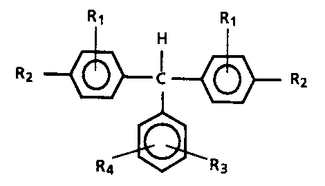
Hydroxy triphenyl methane stabilizer molecules of this invention
is represented by the generic formula shown in FIG. 4 wherein R,, R2, R3, and
R,, are independently selected from the group consisting of:
_19_
2~3427s
-CH3, -H, -OH, -N(CH2CH3),
Rg
wherein R8, R9, and R,a are independently
- C - Rg selected from H or -(CHZ-)n"'CH3 wherein n"'
is an integer from 0 to 6,
R10
R5
wherein Rs and Re are independently
- N selected from the group consisting of
H and -(CHz)"....CH3 wherein n"" is an
R6 integer from 0 to 6,
R~
wherein R~ is independently selected from
--N H or -(CH2)".....CH3 wherein n""' and m are
an integer from 0 to 6,
(CH2)mCH3
-N(CH3)CHZCH20H, -N(CH2)~CH3(CH2)~-OH wherein n is an
integer from 0 to 6 and n' is an integer from 1 to 6, and
-N[(CHZ)n"CH20H]2 wherein n" is an integer from 0 to 6,
wherein at least one or more of R~, R2, R3, or R4 must contain at least one
hydroxy group, and wherein at least one or more of R~, R2, R3, or R4 must
contain at least one amino group.
-20-
2134276
Typical hydroxy triphenyl methane stabilizer molecules are represented
by the formulae in FIGS. 5 through 14. A species represented by the formula
shown in FIG. 5 is, for example, bis-(4-diethylamino-2-methyl phenyl)-4-
hydroxy phenyl methane.
Any suitable alcohol may be employed to apply the overcoating
composition of this invention. The alcohol selected should dissolve the
hydroxy
triphenylmethane and the polyamide utilized in the overcoating layer. The
alcohol solvent should not dissolve any binder in the underlying layer. The
use
of an alcohol solvent minimizes the impact of the coating process on the
1 o environment. The alcohol should contain at least one hydroxy functional
group
per molecule. Typical alcohols containing at least one hydroxy functional gmup
per molecule include, for example, isopropanol, methanol, ethanol, butanol, n-
propanol, and the like. Alcohols with more than one hydroxy group per
molecule include, for example, glycol, and the like. , Satisfactory results
may be
achieved when the amount of alcohol utilized is between about 99 percent by
weight and about 70 percent by weight based on the total weight of the coating
composition. Generally, the optimum amount of alcohol utilized depends upon
the particular type of coating process utilized to apply the overcoating
material.
The concentration of the hydmxy triphenyl methane molecule in the
2 0 overcoat layer may be between about 5 percent and about 50 percent by
weight
and more preferably between about 5 percent and about 50 percent by weight
based on the total weight of the dried overcoat, the remainder normally being
the polyamide binder. When less than about 5 percent by weight of hydroxy
triphenyl methane molecule is present in the overcoat, the charge transport
2 5 through the overcoat slows down resulting in higher residuals. When the
proportion of hydroxy triphenylmethane small molecule charge transport
material in the overcoating layer is greater than about 50 percent by weight
based on the total weight of the overcoating layer, increases in residual
voltages
can be seen with long term cycling. In addition, mechanical and abrasive wear
3 o properties can be negatively impacted.
Any suitable coating technique may be utilized to form the overcoating
layer. Typical coating techniques include spraying, extrusion
21
A
~1342~6
coating, roll coating, veneer coating, dip coating, slide coating, slot
coating, wire wound rod coating, and the like.
Any suitable technique may be utilized to dry the overcoating.
Typical drying techniques include oven drying, forced air oven drying,
radiant heat drying, and the like.
The thickness of the dried overcoat layer should be uniform and
continuous. It can range in thickness from a mono molecular thickness up
to a maximum thickness of about 10 micrometers. Generally, thicker
coatings may be utilized for slower electrophotographic copier and
printers.
If desired, the outer surface of the overcoating layer may be
imparted with a texture to minimize the formation of moray patterns. The
texture may be achieved by any suitable means such as embossing,
regulation of drying conditions, and the like.
Generally, when large amounts of a charge transporting
molecule material is added to an overcoating layer, the strength of the
overcoating layer is reduced. Surprisingly, the overcoating layer of this
invention becomes tougher when large amounts of small molecule
triphenyl methane charge transport material having at least one, but
preferably two hydroxy functional groups are incorporated into the
overcoating layer of this invention. Vllhen triphenyl methane charge
transport material having at least two hydroxy functional groups are
blended with polyamide binder capable of hydrogen bonding to achieve
hydrogen bonding, the combination of materials restricts the absorption of
atmospheric moisture into the polyamide polymer thereby eliminating the
plasticizing effect of the water. Moisture tends to lessen overcoating
abrasion and wear resistance when the overcoating contains only the
polyamide. Unlike coatings containing small molecule charge transport
material dissolved or molecularly dispersed in polycarbonate binder, the
hydrogen bonded overcoat layer is compositionally stable and does not
phase separate even when exposed to liquid ink media.
The film forming binder for the transport layer should not
dissolve in the alcohol solvent selected for the overcoating layer. For
_22_
2'~342~6
example, charge transport layer binders such as polycarbonates do not
dissolve in alcohol. Thus, for example, poly(4,4'-isopropylidene-
diphenylene) carbonate (i.e. bisphenol-A-polycarbonate) shown in FIG. 2 or
poly(4,4'-cyclohexylidine-diphenylene) carbonate (also referred to as
bisphenol-Z-polycarbonate), having a structure represented by the formula
shown in FIG. 15, do not dissolve in alcohols such as isopropanol, methanol,
and the like. Bisphenol-A-polycarbonate dissolves in methylene chloride
and bisphenol-Z-polycarbonate is soluble in toluene. Other polymers
insoluble in alcohols include, for example polystyrene, and the like. The
expression "soluble" as employed herein is defined as capable of forming a
solution with which a film can be applied to a surface and dried to form a
continuous coating. The expression "insoluble" as employed herein is
defined as not capable of forming a solution so that the solvent and the
solid remain in two separate phases and a continuous coating cannot be
formed. Molecular weights of the polymers can vary, for example, from
about 20,000 to about 150,000.
The composition and materials employed in the overcoat layer
must meet several requirements: (1) it should be charge transporting to
prevent a residual build up across the overcoat, and (2) it should not
intermix into the charge transport layer during the process of fabricating
the overcoat and (3) it should have hydroxy groups in order to facilitate
hydrogen bonding with polyamides. The second requirement can be met
by the judicious selection of binders for the charge transport layer and the
overcoat layers whereby the polymer binder for the overcoat is soluble in a
solvent in which the polymer binder for the charge transport layer is
insoluble.
Other suitable layers may also be used such as a conventional
electrically conductive ground strip along one edge of the belt or drum in
contact with the conductive surface of the substrate to facilitate connection
of the electrically conductive layer of the photoreceptor to ground or to an
electrical bias. Ground strips are well known and usually comprise
conductive particles dispersed in a film forming binder.
-23-
1 ~ 4 ~'~ 6
In some cases an anti-curl back coating may be applied to the
side opposite the photoreceptor to provide flatness and/or abrasion
resistance for belt or web type photoreceptors. These anti-curl back
coating layers are well known in the art and may comprise thermoplastic
organic polymers or inorganic polymers that are electrically insulating or
slightly semiconducting.
The photoreceptor of this invention may be used in any
conventional electrophotographic imaging system. As described above,
electrophotographic imaging usually involves depositing a uniform
electrostatic charge on the photoreceptor, exposing the photoreceptor to a
light image pattern to form an electrostatic latent image on the
photoreceptor, developing the electrostatic latent image with
electrostatically attractable marking particles to form a visible toner image,
transferring the toner image to a receiving member and repeating the
depositing, exposing, developing and transferring steps at least once.
A number of examples are set forth hereinbelow and are
illustrative of different compositions and conditions that can be utilized in
practicing the invention. All proportions are by weight unless otherwise
indicated. It will be apparent, however, that the invention can be practiced
with many types of compositions and can have many different uses in
accordance with the disclosure above and as pointed out hereinafter.
TEST PROCEDURES UTILIZED IN FOLLOWING EXAMPLES
Scanner Characterization
Each photoconductor device to be evaluated is mounted on a
cylindrical aluminum drum substrate which is rotated on a shaft. The device
is charged by a corotron mounted along the periphery of the drum. The
surface potential is measured as a function of time by capacitively coupled
voltage probes placed at different locations around the shaft. The probes
are calibrated by applying known potentials to the drum substrate. The
devices on the drums are exposed by a light source located at a position
near the drum downstream from the corotron. As the drum is rotated, the
-24-
~1342'~6
initial (pre-exposure) charging potential is measured by voltage probe 1.
Further rotation leads to the exposure station, where the photoconductor
device is exposed to monochromatic radiation of known intensity. The
device is erased by light source located at a position upstream of charging.
The measurements made include charging of the photoconductor device in
a constant current or voltage mode. The device is charged to a negative
polarity corona. As the drum is rotated, the initial charging potential is
measured by voltage probe 1. Further rotation leads to the exposure
station, where the photoconductor device is exposed to monochromatic
radiation of known intensity. The surface potential after exposure is
measured by voltage probes 2 and 3. The device is finally exposed to an
erase lamp of appropriate intensity and any residual potential is measured
by voltage probe 4. The process is repeated with the magnitude of the
exposure automatically changed during the next cycle. The photodischarge
characteristics is obtained by plotting the potentials at voltage probes 2
and 3 as a function of light exposure. The charge acceptance and dark
decay can also be measured in the scanner.
Parking Deletion Test
A negative corotron is operated (with high voltage connected to
the corotron wire) opposite a grounded electrode for several hours. The
high voltage was turned off, and the corotron was placed (or parked) for
five to ten minutes on a segment of the photoconductor device being
tested. Only a short middle segment of the device was thus exposed to the
corotron effluents. Unexposed regions on either side of the exposed
regions were used as controls. The photoconductor device was then tested
in a scanner for positive charging properties for systems employing donor
type molecules. These systems were operated with negative polarity
corotron in the latent image formation step. An electrically conductive
surface region (excess hole concentration) appeared as a loss of positive
charge acceptance or increased dark decay in the exposed regions
(compared to the unexposed control areas on either side of the short
middle segment) Since the electrically conductive region was located on the
-25-
21 3 4 2.'~ 6
surface of the device, a negative charge acceptance scan was not affected
by the corotron effluent exposure (negative charges do not move through
a charge transport layer made up of donor molecules). However, the excess
carriers on the surface cause surface conductivity results in loss of image
resolution and, in severe cases, causes deletion. The loss of positive charge
acceptance is a measure of deletion with higher loss causing more deletion.
EXAMPLE I
Four electrophotographic imaging members were prepared by
forming coatings using conventional coating techniques on a substrate
comprising a vacuum deposited titanium layer on a polyethylene
terephthalate film (Melinex~, available from ICI). The first applied coating
was a siloxane barrier layer formed from hydrolyzed gamma
aminopropyltriethoxysilane having a thickness of 0.005 micrometer (50
Angstroms). This film was coated as follows: 3-aminopropyltriethoxysilane
(available from PCR Research Chemicals of Florida) was mixed in ethanol in
a 1:50 volume ratio. The film was applied to a wet thickness of 0.5 mil by a
multiple clearance film applicator. The layer was then allowed to dry for 5
minutes at room temperature, followed by curing for 10 minutes at 110
degree centigrade in a forced air oven. The second coating was an adhesive
layer of polyester resin (49,000, available from E. I. duPont de Nemours &
Co.) having a thickness of 0.005 micrometer (50 Angstroms) and was coated
as follows: 0.5 gram of 49,000 polyester resin was dissolved in 70 grams of
tetrahydrofuran and 29.5 grams of cyciohexanone. The film was coated by
a 0.5 mil bar and cured in a forced air oven for 10 minutes. The next coating
was a charge generator layer containing 35 percent by weight vanadyl
phthalocyanine particles obtained by the process as disclosed in US-A
4,771,133 to Liebermann et al., issued September 13, 1988, dispersed in a
polyester resin (Vitel PE100, available from Goodyear Tire and Rubber Co.)
having a thickness of 1 micrometer.
-26-
~1342~fi
EXAMPLE 2
The generator layers of two of the imaging members of Example
1 were coated with a transport layer formed with a solution containing 9
grams of N,N'-Biphenyl-N,N'-bis(3-methyl-phenyl)-(1,1'biphenyl)-4,4'-
diamine and 9 grams of polycarbonate resin [poly(4,4'-isopropylidene-
diphenylene carbonate, available as Makrolon R from Farbenfabricken
Bayer A. G.J, dissolved in 102 grams of methylene chloride solvent using a 3
mil bar. The N,N'-Biphenyl-N,N'-bis(3-methyl-phenyl)-(1,1'biphenyl)-4,4'-
diamine is an electrically active aromatic diamine charge transport small
molecule whereas the polycarbonate resin is an electrically inactive film
forming binder. The coated devices were dried at 80°C for 30 minutes in
a
forced air oven to form a 25 micrometerthick transport layer.
EXAMPLE 3
The generator layers of two of the imaging members of Example
1 were coated with a 25 micrometer thick transport layer of polyether
carbonate. The polyether carbonate resin (structure shown in FIG. 16) was
prepared as described in Example III of US-A Patent 4,806,443. It was
accomplished by dissolving one gram of the polymer into nine grams of
methylene chloride and coating a 25 micrometer film with bar coating. The
films were dried in a forced air oven at 100°C for 20 minutes.
EXAMPLE4
One of the photoreceptor samples of Example 2 was coated with
an overcoat of 50 percent by weight polyamide by dissolving 1 gram of
Elvamide 8061 (available from duPont de Nemours & Co.) and 1 gram of bis-
(4-(beta-hydroxyethyl ethylamino)-2-methylphenyl)phenylmethane (a
dihydroxy triphenyl methane, the structure of which is shown in FIG. 11) in
8 grams of methanol and 8 grams of propanol. The coated device was dried
for 30 minutes by vamping the temperature between 35°C and 100°C
in a
forced air oven to form a 2-3 micrometer thick overcoat layer. This device
was tabled # 1.
_27_
~1342~fi
The second of the photoreceptor samples of Example 2 was
coated with an overcoat of 50 percent by weight polyamide by dissolving 1
gram of Elvamide 8061 (available from duPont de Nemours & Co.) and 1
gram of N,N'-Biphenyl-N,N'-bis(3-hydroxyphenyl)-[1,1'-biphenyl]-4,4'-
diamine (a dihydroxy arylamine of prior art) in 8 grams of methanol and 8
grams of propanol. The coated device was dried 30 minutes by ramping the
temperature between 35°C and 100°C in a forced air oven to form
a 2-3
micrometer thick overcoat layer. This device was labeled # 2.
EXAMPLE 5
One of the photoreceptor samples of Example 3 was coated with
an overcoat of 50 percent by weight polyamide by dissolving 1 gram of
Eivamide 8061 (available from duPont de Nemours & Co.) and 1 gram of
bis-(4-(beta-hydroxyethyl ethylamino)-2-methylphenyl)phenylmethane (a
dihydroxy triphenyl methane, the structure of which is shown in FIG. 11) in
8 grams of methanol and 8 grams of propanol. The coated device was dried
30 minutes by vamping the temperature between 35°C and 100°C in
a
forced air oven to form a 2-3 micrometer thick overcoat layer. This device
was labeled # 3.
The second of the photoreceptor samples of Example 3 was
coated with an overcoat of 50 percent by weight polyamide by dissolving 1
gram of Elvamide 8061 (available from duPont de Nemours & Co.) and 1
gram of N,N'-Biphenyl-N,N'-bis(3-hydroxyphenyl)-[1,1'-biphenyl]-4,4'-
diamine (a dihydroxy arylamine of prior art) in 8 grams of methanol and 8
grams of propanol. The coated device was dried 30 minutes by vamping the
temperature between 35°C and 100°C in a forced air oven to form
a 2-3
micrometer thick overcoat layer. This device was labeled # 4.
EXAMPLE 6
Devices # 1, 2 ,3 and 4 were tested in a scanner. The Photo-
Induced Discharge (PIDC) characteristics of devices # 1 and 2 were
equivalent to each other. The Photo-Induced Discharge (PIDC)
characteristics of devices # 3 and 4 were equivalent to each other.
-28_
1342~'~
EXAMPLE 7
Devices # 1, 2 ,3 and 4 were subjected to the "Parking Deletion
Test" described above. Before exposure to corona charging, the positive
potential on all four photoreceptors were essentially equivalent (800 V).
After corona exposure for 10 minutes, Devices 2 and 4 (prior art) showed
deletion with a loss of positive potential (400V) in the center region of the
samples whereas Devices 1 and 3 (devices of the present invention) showed
essentially no deletion (no loss of positive potential). In addition, the
sample overcoated with polyamide and dihydroxy arylamine also showed
loss of potential on the regions bordering each side of the exposed region.
This demonstrates the sensitivity of the polyamide and dihydroxy arylamine
surface (as compared to the nonovercoated control sample) to corona
effluents that diffuse on either side of the parked corotron. The device
overcoated with polyamide and bis-(4-(beta-hydroxyethyl ethylamino)-2-
methylphenyl)phenylmethane of the present invention showed no
deletion. Later, 14 hours after exposure, the sample overcoated with
polyamide and dihydroxy aryiamine still exhibited some deletion in the
parking deletion test.
Although the invention has been described with reference to
specific preferred embodiments, it is not intended to be limited thereto,
rather those skilled in the art will recognize that variations and
modifications may be made therein which are within the spirit of the
invention and within the scope of the claims.
_29_