Note: Descriptions are shown in the official language in which they were submitted.
t_2134277
VIDEO FORMAT CONVERSIONS SYSTEMS
BACKGROUND OF THE INVENTION
Field of the Invention
The present invention relates to image processing
apparati, and more particularly, to an image processing
apparatus suitable for computer systems such as a personal
computer and a workstation, domestic information terminals
such as a HA (Home Automation) system and portable
information terminals, and also communication systems of
television, telephones and television conferences.
Description of the Background Art
A conventional image processing apparatus compresses
image data by converting a video signal from a video movie
camera or the like into an intermediate format called a
CIF (Common Intermediate Format). The compressed image
data is transmitted to the other side via a telephone
line.
Such an image processing apparatus will be described
hereinafter with reference to Figure 71 showing a
structure of a conventional image processing apparatus.
Referring to Figure 71, an image processing apparatus
-1-
B
2134277
includes a video movie 201, an A/D converter 202, a
luminance signal processing circuit 203, a color signal
processing circuit 204, an image conversion circuit 205,
and a frame memory 206.
An analog video signal or a YC separation signal from
video movie 201 is converted into a digital video signal
by A/D converter 202. Digital luminance signal Y and
digital color signal C of the digital video signal are
processed by luminance signal processing circuit 203 and
color signal processing circuit 204, respectively, to be
provided to image conversion circuit 205. The digital
video signals processed by each of processing circuits 203
and 204 are stored in frame memory 206 via image
conversion circuit 205. Image conversion circuit 205
reads out the digital video signal stored in frame memory
206 to convert the same into a CIF format by applying
frame frequency conversion, line conversion, and pixel
conversion thereto. Such a conventional image processing
apparatus is disclosed in for example, Japanese Patent
Laying-Open Nos. 4-229789 and 4-185087.
Because such a conventional image processing
apparatus has to carry out complicated frame frequency
conversion, pixel conversion, and line conversion, the
circuit complexity thereof is increased. There was also a
problem that a frame memory is required. Furthermore,
-2-
2134277
when an arbitrary image format conversion is to be carried
out, the storage capacity required for the frame memory is
increased, resulting in greater circuit complexity. When
compressed image data is to be generated by skipping the
image data, the converted image is reduced in size, and
there was a possibility of distortion in the resulting
image. -
SUMMARY OF THE INVENTION
An object of the present invention is to provide an
image processing apparatus that can provide image data of
high quality without increasing memory capacity and
circuit complexity.
An image processing apparatus according to an aspect
of the present invention includes an image signal output
unit for converting image sensed light incident from an
object into a digital image signal and outputting the
image signal, a signal processing circuit for applying
signal process on the digital image signal to output a
digital video signal, and a conversion circuit for
converting the digital video signal into image data
corresponding to a predetermined image format.
According to the above-described structure, image
sensed light incident from an object is directly converted
into a digital image signal, the converted digital image
signal is subjected to a signal process to be converted
-3-
213477
into a digital video signal, and then further converted
into image data corresponding to a predetermined image
format. Therefore, the memory capacity and the circuit
complexity are not increased, and image data of high
quality can be output.
An image processing apparatus according to another
aspect of the present invention includes: an image signal
output unit for converting image sensed light incident
from an object into a digital image signal and outputting
the same; a memory for storing program data corresponding
to a predetermined video system; and a signal processing
logic circuit that can have an arbitrary logic programmed.
The signal processing logic circuit has a predetermined
logic programmed according to program data stored in the
memory, and converts a digital image signal into a digital
video signal of a predetermined video system.
According to the above-described structure, an
arbitrary logic can be programmed in a signal processing
logic circuit, and a digital image signal can be converted
into a digital video signal corresponding to a desired
video system to be output. As a result, the storage
capacity and the circuit complexity are not increased, and
image data of high quality can be output.
An image processing apparatus according to a further
aspect of the present invention includes: an image signal
-4-
m3~z~~
output unit for converting image sensed light incident
from an object into a digital image signal to output the
same; an input unit for applying program data
corresponding to a predetermined video system input from
an external device into a main body of the apparatus; and
a signal processing logic circuit that can have an
arbitrary logic programmed. The signal processing logic
circuit has a predetermined logic programmed according to
program data input from an external device via the input
unit, and a digital image signal is converted into a
digital video signal corresponding to the predetermined
video system to be output.
According to the above-described structure, an
arbitrary logic can be programmed in a signal processing
logic circuit from an external device, and a digital image
signal is converted into a digital video signal according
to a desired video system to be output. As a result,
image data of high quality can be output without
increasing storage capacity and circuit complexity.
The foregoing and other objects, features, aspects
and advantages of the present invention will become more
apparent from the following detailed description of the
present invention when taken in conjunction with the
accompanying drawings.
BRIEF DESCRIPTION OF THE DRAWINGS
-5-
213427
Fig. 1 is a block diagram showing a structure of an
image processing apparatus according to a first embodiment
of the present invention.
Fig. 2 is a block diagram showing a structure of a
first specific example of the image conversion circuit of
Fig. 1.
Figs. 3 and 4 are block diagrams showing a structure
of the main components of an image processing apparatus
according to a second embodiment and a third embodiment,
respectively, of the present invention.
Fig. 5 is a block diagram showing a specific
structure of the main components of the image processing
apparatus of Fig. 4.
Fig. 6 is a block diagram showing a structure of the
main components of an image processing apparatus according
to a fourth embodiment of the present invention.
Fig. 7 is a block diagram showing a specific
structure of the main components of the image processing
apparatus of Fig. 6.
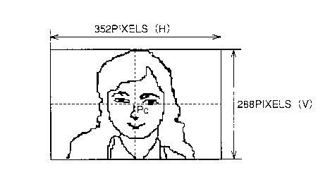
Fig. 8 is a diagram for describing the center
coordinates Pc of a face.
Fig. 9 is a block diagram showing a structure of an
image conversion circuit of an image processing apparatus
according to a fifth embodiment of the present invention.
Fig. 10 is a block diagram showing a first specific
-6-
.. . 213 ~ ~'~'~
example of a data 1/2 conversion circuit of Fig. 9.
Figs. 11 and 12 are first and second timing charts
for describing the operation of the data 1/2 conversion
circuit of Fig. 10.
Fig. 13 is a block diagram showing a second specific
structure of the data 1/2 conversion circuit of Fig. 9.
Fig. 14 is a timing chart for describing the
operation of the data 1/2 conversion circuit of Fig. 13.
Fig. 15 is a block diagram showing a structure of an
image conversion circuit of an image processing apparatus
according to a sixth embodiment of the present invention.
Fig. 16 is a block diagram showing a structure of an
SIF conversion circuit of Fig. 15.
Fig. 17 is a timing chart for describing the
operation of the SIF conversion circuit of Fig. 16.
Figs. 18 and 19 are block diagrams showing a
structure of an image conversion circuit of an image
processing apparatus according to a seventh embodiment and
an eighth embodiment, respectively, of the present
invention.
Fig. 20 is a block diagram showing a structure of an
image processing apparatus according to a ninth embodiment
of the present invention.
Fig. 21 is a block diagram showing a structure of an
image conversion circuit of Fig. 20.
_. 21342~~
Fig. 22 is a block diagram showing a structure of a
vertical conversion circuit of Fig. 21.
Fig. 23 is a timing chart for describing an operation
of the vertical conversion circuit of Fig. 22.
Fig. 24 is a block diagram showing a structure of an
horizontal conversion circuit of Fig. 21.
Fig. 25 is a block diagram showing a structure of a
calculation circuit of Fig. 24.
Fig. 26 is a timing chart for describing the
operation of the horizontal conversion circuit of Fig. 24.
Fig. 27 is an output timing chart of a case where
conversion is carried out by the horizontal conversion
circuit of Fig. 24.
Fig. 28 is a block diagram showing a structure of a
data control circuit.
Fig. 29 is a block diagram showing a structure of an
image processing circuit according to a tenth embodiment
of the present invention.
Fig. 30 is a block diagram showing a structure of an
image conversion circuit of Fig. 29.
Figs. 31 and 32 are first and second timing charts of
an input signal into the image conversion circuit of Fig.
29.
Figs. 33 and 34 are timing charts for describing a
vertical conversion operation and a horizontal conversion
_g_
2~342'~'~
operation, respectively, of the image conversion circuit
of Fig. 29.
Fig. 35 is a block diagram showing another specific
structure of the image conversion circuit of Fig. 29.
Fig. 36 is a timing chart for describing the
operation of an QVGA conversion circuit of Fig. 35.
Fig. 37 is a block diagram showing a structure of a
calculation circuit that carries out horizontal 1/2
conversion.
Fig. 38 is a block diagram showing a structure of a
Q'~7GA shown in Fig. 35.
Figs. 39 and 40 are first and second timing charts,
respectively, for describing the operation of the QzVGA
shown in Fig. 38.
Fig. 41 is a block diagram showing a structure of a
horizontal 1/2 calculation unit of Fig. 38.
Fig. 42 is a block diagram showing another specific
structure of the QTVGA conversion circuit of Fig. 35.
Fig. 43 is a timing chart for describing the
operation of the QwGA conversion circuit of Fig. 42.
Fig. 44 is a block diagram showing another specific
structure of the image conversion circuit of Fig. 29.
Fig. 45 is a block diagram showing another specific
structure of the horizontal 1/2 calculation unit of Fig.
38.
_g_
~~342~7
Fig. 46 is a block diagram showing a structure of an
image processing apparatus according to an eleventh
embodiment of the present invention.
Fig. 47 is a flow chart for describing a control
operation of an image conversion control circuit of Fig
46.
Figs. 48, 49 and 50 are block diagram showing a
first, a second, and a third, specific structure,
respectively, of the image conversion control circuit of
Fig. 46.
Fig. 51 is a block diagram showing a structure of an
image processing apparatus according to a twelfth
embodiment of the present invention.
Fig. 52 is a flow chart for describing the control
operation of a signal processing unit control circuit of
Fig. 51.
Figs. 53, 54 and 55 are block diagrams showing a
first, a second, and a third specific structure,
respectively, of the digital signal processing circuit of
Fig. 51.
Fig. 56 is a block diagram showing a structure of an
image processing apparatus according to a thirteenth
embodiment of the present invention.
Fig. 57 is a flow chart for describing the control
operation of the control circuit of Fig. 56.
-10-
2I342?~
Fig. 58 is a block diagram showing a structure of an
image processing apparatus according to a fourteenth
embodiment of the present invention.
Figs. 59, 60, and 61 are block diagrams showing a
first, a second, and a third specific structure,
respectively, of the image processing apparatus shown in
Fig. 58.
Figs. 62 and 63 are block diagrams showing a
structure of an image processing apparatus of a fifteenth
embodiment and a sixteen embodiment, respectively, of the
present invention.
Fig. 64 is a flow chart for describing a FPGA
programming method of the image processing apparatus of
Fig. 63.
Fig. 65 is a block diagram showing a structure of an
image processing apparatus according to a seventeenth
embodiment of the present invention.
Figs. 66 and 67 are circuit diagrams of a first and a
second structure, respectively, of a register in a
register unit shown in Fig. 65.
Fig. 68 is a block diagram showing a structure of an
image processing apparatus according to an eighteenth
embodiment of the present invention.
Figs. 69 and 70 are block diagrams showing first and
second specific structures, respectively, of the image
-11-
213477
processing apparatus of Fig. 68.
Fig. 71 is a block diagram showing a structure of a
conventional image processing apparatus.
DESCRIPTION OF THE PREFERRED EMBODIMENTS
An image processing apparatus according to a first
embodiment of the present invention will be described
hereinafter.
Referring to Fig. 1, an image processing apparatus
includes an image sensing device 1, a pre-processing
circuit 2, an A/D conversion circuit 3, a video signal
processing circuit 4, an image conversion circuit 5, a
control circuit 6, and a drive circuit 7.
Image sensing device 1 converts image sensed light
captured by an internal lens (not shown) into an
electrical signal. Pre-processing circuit 2 sample-holds
a signal output from image sensing device 1 and applies a
process such as automatic gain control (AGC) on the
sample-held output signal. A/D conversion circuit 3
converts an output signal of pre-processing circuit 2 into
digital data in the units of pixels, and provides a
digital image signal DI.
Video signal processing circuit 4 generates a
luminance signal Y, and color signals R-Y, B-Y on the
basis of a digital image signal DI output from A/D
conversion circuit 3, and provides the same as a digital
-12-
2Z342~7
video signal DP. Here, video signal processing circuit 4
carries out white balance process, gamma correction, and
the like, whereby luminance signal Y and color signals R-Y
and B-Y are output as digital signals. Here, the color
signals are output as dot sequential color difference of
R-Y/B-Y.
Drive circuit 7 generates a pulse such as a drive
timing pulse, a video signal synchronizing pulse, and a
video signal processing pulse to control the operation of
image sensing device 1. Control circuit 6 controls the
operation of A/D conversion circuit 3, video signal
processing circuit 4, image conversion circuit 5, and
drive circuit 7. Image conversion circuit 5 converts
luminance signal Y and color signals R-Y and B-Y output
from video signal processing circuit 4 into image data FD
of a screen size specified by control circuit 6 which is
output to an external source. The screen size is
externally input into control circuit 6.
A circuit that carries out conversion into a CIF
format will be described in detail hereinafter as an image
conversion circuit. A CIF format is a common video signal
format on the basis of video codec intercommunication
conforming to the coding system employed in H.261 or the
like. A luminance sample of a CIF format is arranged in
an orthogonal grid array with 352 pixels per line and 288
-13-
~~~4z77
lines per frame. Each sample of the two color difference
components are arranged in an orthogonal grid array with
176 pixels per line and 144 lines per frame. The above-
described image region has an aspect ratio of 4:3, and
matches the valid screen of a standard television signal.
The number of frames per second is 30.
A CIF format conversion will be described hereinafter
using an image sensing device of 320000 pixels. Here, the
number of pixels of the image sensing device is 512(H) x
582(V).
According to control circuit 6 and drive circuit 7, a
non-interlaced read out electrical signal is output from
image sensing device 1. This electrical signal is
converted into a digital video signal DP by pre-processing
circuit 2, A/D conversion circuit 3, and video signal
processing circuit 4, whereby luminance data and color
data (dot sequential color difference) of 512(H) x 291(V)
pixels are obtained. Image conversion circuit 5 generates
image data FD of 352(H) x 288(V) pixels corresponding to a
CIF format according to the obtained luminance data and
color data.
The above image conversion circuit will be described
in detail with reference to Fig. 2. Referring to Fig. 2,
an image conversion circuit includes a line processing
unit 51, a horizontal luminance processing unit 52, and a
-14-
zi~4z~~
horizontal color processing unit 53. Horizontal luminance
processing unit 52 includes a shift circuit 521, a
luminance memory circuit 522, a luminance skipping unit
523, a luminance buffer circuit 524, and a luminance FIFO
(First-In and First-Out) 525. Horizontal color processing
unit 53 includes a shift circuit 531, a color memory
circuit 532, a color skipping unit 533, a color buffer
circuit 534, and a color FIFO 535.
First, line processing unit 51 dicards 3 lines of
data from the luminance data and the color data of 291
lines to result in data of 288 lines. This conversion can
be realized by, for example, providing an internal counter
to count a line synchronizing signal, and making valid
only data of 288 lines.
Then, for each of the 288 lines of image data output
from line processing unit 51, a skipping process in the
horizontal direction is carried out for each line. More
specifically, the luminance data is converted from 512
pixels to 352 pixels, and each color data is converted
from 256 pixels to 176 pixels.
As to this conversion process, first the operation of
horizontal luminance processing unit 52 will be described.
Here, luminance data Yin is applied to a skipping process
for every 32 pixels to generate data of 22 pixels. First,
an input luminance data Yin is shifted by 1 clock by shift
-15-
circuit 521 in synchronization with a clock CLK1. When 32
pixels are shifted, the shifted luminance data Yin is
stored int o luminance memory circuit 522 in
synchroniz ation with a clock CLK1/32. Luminance skipping
unit 523 onverts luminance data YO-Y31 of 32 pixels into
c
luminance data Y'0-Y'21 of 22 pixels as set forth in the
following.
Y'0 = YO
Y' 1 = Y1 + Y2
Y'2 = Y3
Y'3 = Y4 + Y5
Y'4 - Y6
Y'S - Y7 + Y8
Y'6 - Y8 + Y9
Y'7 - Y10 + Y11
Y'8 = Y11 + Y12
Y'9 - Y13
Y'10 = Y14 + Y15
Y'll = Y16
Y'12 = Y17 + Y18
Y'13 = Y19
Y'14 - Y20 + Y21
Y'15 = Y22
Y'16 - Y23 + Y24
Y'17 - Y24 + Y25
-16-
21~~~~7
Y'18 = Y26 +
Y27
Y'19 - Y27 +
Y28
Y'20 = Y29
Y'21 = Y30 +
Y31
By carrying the above-described conversion operation
16 times, the pixels are converted from 512 pixels to 352
pixels, resulting in a skipping process for 1 line. By
carrying this operation for the 288 lines, image data
corresponding to a CIF format can be obtained.
The converted luminance data Y'0-Y'21 are stored into
luminance buffer circuit 524 in synchronization with a
clock CLK1/32. Then, luminance data Y'0-Y'21 are
transferred to luminance FIFO 525, and then externally
output as luminance data CLFYout in synchronization with a
transfer clock CLK2.
Color data is also processed by horizontal color
processing unit 53 in parallel to the above-described
process. Color data R-Y and B-Y input from line
processing unit 51 are respectively shifted by 16 pixels
by shift circuit 531. The color data is stored into color
memory circuit 532 in synchronization with clock CLK1/32.
The stored color data R-YO~R-Y15 and B-YO~B-Y15 are
converted into color data R-Y'0~R-Y'10 and B-Y'0~B-Y'10
according to the following skipping process, similar to
luminance signal, by color skipping unit 533.
-17-
2~3~277
(R-Y'0) - R-YO
(R-Y'1) - R-Y2
(R-Y'2) - R-Y3
(R-Y'3) - R-Y4
(R-Y'4) - R-Y6
(R-Y'S) - R-Y7
(R-Y'6) - R-Y9
(R-Y'7) - R-Y10
(R-Y'8) - R-Y12
(R-Y'9) - R-Y13
(R-Y'10) - R-Y15
(B-Y'0) - B-YO
(B-Y'1) - B-Y2
(B-Y'2) - B-Y3
(B-Y'3) - B-Y4
(B-Y'4) - B-Y6
(B-Y'S) - B-Y7
(B-Y'6) - B-Y9
(B-Y'7) - B-Y10
(B-Y'8) - B-Y12
(B-Y'9) - B-Y13
(B-Y'10) - B-Y15
By carrying out the above-described conversion
operation 16 times, the data is converted from 256 pixels
into 176 pixels, resulting in a skipping process of 1
-18-
~~342~?
line. This conversion operation is carried out only for
the 256 pixels. By carrying out the above-described
operation for the 288 lines, an image size corresponding
to a CIF format is obtained.
The converted color data R-Y'0~R-Y'll and B-Y'0~B-
Y'll are stored into color buffer circuit 534 in
synchronization with clock CLK 1/32. Then, color data R-
Y'0~R-Y'll and B-Y'0~B-Y'll are transferred to color FIFO
535, and then externally output as color data CIFCout in
synchronization with transfer clock CLK2.
The luminance data and the color data processed as
described above are output for every 1 line as a data
pair. Thus, image conversion data corresponding to an
externally specified format, for example a CIF format, can
be output.
An image processing apparatus according to a second
embodiment of the present invention will be described
hereinafter.
Referring to Fig. 3, the image processing apparatus
of the second embodiment has a memory 8 added in image
conversion circuit 5. Memory 8 stores field data (digital
video data) output from video signal processing circuit 4.
In the above-described first embodiment, image data is
processed for every 1 field (odd number field or even
number field), so that only 1/2 vertical lines of 1 frame
-19-
213 4 2'~'~
can be obtained in a non-interlace process. The second
embodiment has interlaced input image data converted into
non-interlaced image data, whereby image conversion
circuit 5 converts the same into an externally specified
image format. As a result, a maximum number of vertical
lines of 1 frame can be obtained. The conversion process
of the image format is similar to that of the first
embodiment.
An image processing apparatus according to a third
embodiment of the present invention will be described
hereinafter with reference to Fig. 4. The image
processing apparatus of the third embodiment includes an
image detection circuit 9 in addition to the structure of
the second embodiment. Memory 8 stores video data. Image
detection circuit 9 is a circuit for detecting the feature
of the image of the video data applied from video signal
processing circuit 4. For example, determination is made
whether the image is mainly of a person, text, or whether
it is a still picture or a moving picture. In the third
embodiment, image conversion circuit S selects a
predetermined image conversion method according to the
determination result of video detection circuit 9.
A specific structure of the main components of the
image processing apparatus shown in Fig. 4 will be
described hereinafter. Referring to Fig. 5, the image
-20-
213427?
processing apparatus includes a binarization processing
circuit 91, a frame difference detection unit 92, a frame
memory 93, an image area detection unit 94, and an image
conversion circuit 5a. Image conversion circuit 5a
includes a moving picture oriented conversion circuit 54,
a person oriented conversion circuit 55, and a text
oriented conversion circuit 56.
Binarization processing unit 91 converts the
luminance data of the Nth frame applied from video signal
processing circuit 4 into binary data. The binarized data
of the Nth frame is stored in frame memory 93 via frame
difference detection unit 92. Frame difference detection
unit 92 compares the binary data of the Nth frame stored
in frame memory 93 and the subsequent input binary data of
the (N+1)th frame. By this comparison, frame difference
detection unit 92 detects whether there is movement
between the frames. Next, binary data of the (N+1)th
frame is stored into frame memory 93. Then, the above-
described operation is sequentially carried out. Frame
difference detection unit 92 determines whether there is
movement in the input image. Determination is made by
frame difference detection unit 92 that the image is a
moving picture when there is movement, and a still picture
when there is no movement.
Image area detection unit 94 calculates the occupying
-21-
2342??
area of the image on the basis of the binary data output
from frame difference detection unit 92. Determination is
made by image area detection unit 94 that the data is
image data mainly of a person when there is a large image
portion with respect to the image data of 1 frame. In
contrast, if the image portion is small, determination is
made that it is text data. In the case of a moving
picture, the area detection process is not carried out,
and determination is directly made of a moving picture
data.
The determination carried out by image area detection
unit 94 is based on calculating the ratio of black data to
white data in 1 frame using binary data of 1 frame
binarized into either white or black. When black is
great, a process is carried out on the assumption that it
is image data mainly of a person. When white is great, a
process is carried out on the assumption that it is image
data mainly of text.
Image area detection unit 94 applies the image data
into moving picture oriented conversion circuit 54 of
image conversion circuit Sa when determination is made of
a moving image according to the above-described process.
When determination is made of a still picture of a person,
the image data is input into person oriented conversion
circuit 55 in image conversion circuit 5a. The image data
-22-
~~34z7~
is applied to text oriented conversion circuit 56 in image
conversion circuit Sa when determination is made that the
image is a still picture and text image. Thus, the
feature of the input image data is detected, and an image
format conversion process, a filtering process, or the
like is selected according to the determination result.
Thus, an optimum image format conversion process is
realized.
A structure of the main components of an image
processing apparatus according to a fourth embodiment of
the present invention will be described hereinafter with
reference to Fig. 6. The image processing apparatus
according to the fourth embodiment includes a face
tracking circuit 10 instead of image detection circuit 9
of the third embodiment. The image data provided from
video signal processing circuit 4 is applied to face
tracking circuit 10 via image conversion circuit 5. Face
tracking circuit 10 extracts the face of a person
according to the input image data. Image conversion
circuit 5 generates image data of a screen size
corresponding to an externally specified format, for
example a CIF format, with the position of the extracted
face as the center.
By such a process, an image of a face that is reduced
in distortion can be transmitted effectively by conversion
-23-
2~3427~
in the case where image data mainly of a person is
transferred such as on the screen of a television
telephone or television conference.
A specific structure of the main component of the
image processing circuit of Fig. 7 will be described.
Referring to Fig. 7, the image processing apparatus
includes a frame difference detection unit 101, a
binarization processing unit 102, frame memories 103 and
105, a face coordinate calculation unit 104, an image
conversion circuit 5, and a memory 8.
Digital video data DP input from video signal
processing circuit 4 is applied to frame difference
detection unit 101. Frame difference detection unit 101
compares the image data stored in frame memory 105 and the
image data applied at the next 1 frame to detect the
difference thereof. Frame difference detection unit 101
detects the edge of the moving portion according to the
difference thereof.
The differential data of the moving portion generated
by frame difference detection unit 101 is binarized by
binarization processing unit 102. Binarization processing
unit 102 applies a labeling process on the binary data for
adjustment, and also removes noise. Then, face coordinate
calculation unit 104 calculates the position data of the
face portion, and specifies a face region. Frame memory
-24-
2~~42~7
103 stores the image data of the specified region. On the
basis of this face data, the center coordinates Pc of a
face (refer to Fig. 8) is extracted. According to the
data obtained by the above-described process, image
conversion circuit 5 carries out a zooming or skipping
process so that the entire face fits into the size of the
CIF format (352 pixels x 288 pixels) with the center
coordinates Pc of the face as the center.
By directly applying image conversion on an image
signal output from an image sensing device according to
the present invention, a natural picture with little
distortion in the image can be obtained without increasing
the memory capacity and the circuit complexity in
comparison with the conventional case where image format
conversion is carried out after the image signal is
converted into a NTCS or a PLA analog video signal. Also,
by detecting the position of a face, image format
conversion can be carried out only on a required region in
which a face is extracted, and only the image data
required for an image compression circuit or the like can
be output. Therefore, the image data can be reduced.
Furthermore, because data other than the face that is not
required is not output, the peripheral unrequired image in
a television telephone or the like does not have to be
transferred.
-25-
213~27~
An image processing apparatus according to a fifth
embodiment of the present invention will be described
hereinafter. The following fifth-eighth embodiments are
image processing apparatuses that can obtain image data of
different formats such as CIF, QCIF, SIC and QSIF. Also,
a frame memory is not required, and increase in circuit
complexity can be suppressed. -
Referring to Fig. 9, the image conversion circuit of
the image processing apparatus of the fifth embodiment
includes a CIF conversion circuit 57, and a data 1/2
conversion circuit 58. The other components are similar
to those of the first embodiment shown in Fig 1, and there
details will not be repeated. The image processing
apparatus of the fifth embodiment includes CIF conversion
circuit 57 for converting digital video data DP applied
from a signal processing circuit 4 into a CIF format of
352 dots x 288 lines as shown in Fig. 9. At a subsequent
stage of CIF conversion circuit 57, data 1/2 conversion
circuit 58 is provided as a format conversion circuit that
converts image data CIF corresponding to a CIF format into
image data of another format. More specifically, a
conversion circuit is added that provides image data QCIF
corresponding to a QCIF format of 176 dots x 144 lines by
converting the horizontal information and the vertical
information of the CIF data to 1/2.
-26-
21342~~
A structure of the data 1/2 conversion circuit of
Fig. 9 will be described with reference to Fig. 10.
Referring to Fig. 10, a data 1/2 conversion circuit
includes a dot 1/2 conversion circuit 581, a line 1/2
conversion circuit 582, and an output clock gate 583.
Dot 1/2 conversion circuit 581 reduces only the
horizontal information of image data CIF to 1/2,-and
provides a dot clock signal DCK into output clock gate
583. Line 1/2 conversion circuit 582 reduces only the
vertical information of image data CIF to 1/2, and
provides a line clock signal LCK to output clock gate 583.
Output clock gate 583 receives a timing signal DCLK
applied to image data CIF, in addition to dot clock signal
DCK and line clock signal LCK. Timing signal DCLK is a
reference signal indicating an output timing of a dot.
The operation of the image processing apparatus of
the fifth embodiment will be described with reference to
Figs. 11 and 12. Image data CIF converted into a CIF
format is output from CIF conversion circuit 57 according
to a timing shown in Fig. 11. Image data CIF from CIF
conversion circuit 57 is applied to data 1/2 conversion
circuit 58 which is provided at a succeeding stage of CIF
conversion circuit 57. In Fig. 11, luminance signal Y and
color signal W are signals showing the luminance and
color of image data CIF. Signal LSTN is a signal
-27-
2~3427~
indicating the start of a dot which is the horizontal
information of image data CIF. Signal FSTN is a signal
indicating the start of a line which is the vertical
information of image data CIF. The broken line in Fig. 11
indicates the lines of 1 unit of image data CIF, i.e. the
lines from line 0 to line 287.
When image data CIF is applied to data 1/2 conversion
circuit 58, a line clock signal LCK that is driven to H
(logical high) and L (logical low) for every signal LSTN
is output from line 1/2 conversion circuit 582 as shown in
Fig. 12. From dot 1/2 conversion circuit 581, a first dot
clock signal DCKl driven to H and L for every 1 dot of a
luminance signal and a second dot clock signal DCK2 driven
to H and L for every 2 dots of color signals are
respectively output. Here, when the first dot clock
signal DCK1 and line clock signal LCK both attain H, an
output clock signal YwCLK according to timing signal DCLK
is provided from output clock gate 583. When second dot
clock signal DCK2 and line clock signal LCK both attain H,
an output clock signal UVWCLK according to timing signal
DCLK is provided from output clock gate 583. As a result,
image data QCIF converted into a QCIF format of 176 dots x
144 lines is output from data 1/2 conversion circuit 58 by
having the horizontal and vertical information of image
data CIF respectively converted to 1/2.
-28-
In the fifth embodiment, when data 1/2 conversion
circuit 58 is not operated, image data CIF is directly
output from data 1/2 conversion circuit 58. Therefore, by
selecting whether data 1/2 conversion circuit 58 is to be
operated or not, image data of a CIF format or a QCIF
format can be selectively output.
The present invention is not limited to the fifth
embodiment in which a data 1/2 conversion circuit
including dot 1/2 conversion circuit 581, line 1/2
conversion circuit 583, and output clock gate 583 is
employed, and image data of a CIF format can have the
horizontal information and the vertical information
converted to 1/2 by carrying out a calculation of taking
the average value of two data.
A second specific example of the data 1/2 conversion
circuit of Fig. 9 will be described hereinafter with
reference to Figs. 13-15. The present second example is a
data 1/2 conversion circuit that carries out averaging by
calculation.
Referring to Fig. 13, a data 1/2 conversion circuit
includes a line memory 584, calculation units 585 and 587,
a flipflop 586, and a data timing control circuit 589.
Line memory 584 and calculation circuit 585 process at
least the vertical information of luminance signal Y of
image data CIF input according to the format shown in Fig.
-29-
z~34z~7
11. Similarly, flipflop 586 and calculation unit 587
process the horizontal information.
Data timing control circuit 589 outputs a data enable
signal DE generated according to signal FSTN, signal LSTN
and timing signal DCLK of the image data of the CIF
format. Here, line memory 584 stores vertical data A in
the input line of 1 unit, and provides to calculation unit
585 the stored vertical data A when vertical data B of the
next line of 1 unit is input. Calculation unit 585 merges
vertical data A input from line memory 584 and the next
directly input vertical data B, i.e., carries out a
(A+B)/2 process.
Flipflop 586 operates with timing signal DCLK as a
clock signal. Calculation unit 587 merges horizontal data
A of the line of 1 unit provided from flipflop 586 and the
next input horizontal data B of the line of 1 unit, i.e.,
carries out a (A+B)/2 process. As a result, a luminance
signal of image data CIF subjected to a 1/2 averaging
process in both the horizontal and vertical directions is
output from calculation unit 587.
Data timing control circuit 589 outputs a data enable
signal DE that is rendered to H and to L for every line of
1 unit subsequent to the preceding line of 1 unit
according to signal FSTN, and that is rendered to H and to
L for every dot of 1 unit subsequent to the preceding 1
-30-
23427?
unit according to signal LSTN. The period when data
enable signal DE attains a H level is the active period
for data entry. When data enable signal DE having this
active period is provided together with the image data
output from calculation unit 587, image data QCIF
corresponding to a QCIF format of 176 dots x 144 lines is
output from the data 1/2 conversion circuit of the present
embodiment, similar to that of the fifth embodiment.
An image conversion circuit of an image processing
apparatus according to a sixth embodiment of the present
invention will be described hereinafter. Referring to
Fig. 15, an image conversion circuit includes a CIF
conversion circuit 57, and a SIF conversion circuit 59.
In the sixth embodiment, conversion to a CIF format is
carried out by reducing the image data of a CIF format of
352 dots x 288 lines at the top and bottom 24 lines in the
vertical direction.
The apparatus of the sixth embodiment includes a CIF
conversion circuit 57 that converts a digital video signal
input from a signal processing circuit into a CIF format
of 352 dots x 288 lines, as shown in Fig. 15. At a
succeeding stage of CIF conversion circuit 57, a SIF
conversion circuit 59 that carries out format conversion
is provided. More specifically, a conversion circuit is
provided that converts data of a CIF format into image
-31-
21342'~~
data SIF corresponding to a SIF format of 352 dots x 240
lines.
The SIF conversion circuit of Fig. 15 will be
described hereinafter with reference to Figs. 16 and 17.
Referring to Fig. 16, a SIF conversion circuit includes a
24-line counter 591, a 240-line counter 592, and a line
start detection unit 593. 24-line counter 591 delays the
initiation of the vertical information process of the
image data of the CIF format by 24 lines in the SIF format
conversion operation. 240-line counter 592 detects the
end of the vertical information process.
When a SIF conversion is to be carried out, 24-line
counter 591 receives signal FSTN, as shown in Fig. 17, and
then counts 24 lines of the vertical data of image data
CIF, and delays signal OFSTN as signal FSTN output to an
external source. As a result, vertical data of 24 lines
is removed. Here, 240-line counter 592 detects signal
OFSTN output from 24-line counter 591, and counts 240
lines of the vertical data of the CIF format image data.
Then, 240-line counter 592 provides to line start
detection unit 593 a signal having an active period for
indicating a fetching valid period of the vertical
information.
After detection of signal OFSTN, line start detection
unit 593 externally provides signal OLSTN which is
-32-
2~342~~
obtained corresponding to signal LSTN when the signal
output from 240-line counter 592 is active. As a result,
image data SIF corresponding to a SIF format converted
into 352 dots x 240 lines is output from SIF conversion
circuit 59.
When SIF conversion circuit 59 of the present
embodiment is not operated, image data corresponding to a
CIF format is directly output from SIF conversion circuit
59. Because SIF conversion circuit 59 receives a mode
signal CIFM instructing a CIF conversion instead of a mode
signal SIFM instructing a SIF conversion, 240-line counter
591 receiving mode signal CIFM directly outputs the input
signal FSTN. Therefore, 240-line counter 592 will always
output an active signal. Therefore, image data
corresponding to a CIF format is output without being
subjected to any conversion process by the SIF conversion
circuit. By selecting whether a SIF conversion circuit is
to be operated or not according to a mode signal in the
present embodiment, image data corresponding to a CIF
format or a SIF format can be selectively output.
An image conversion circuit of an image processing
apparatus according to a seventh embodiment of the present
invention will be described hereinafter with reference to
Fig. 18. In the seventh embodiment, conversion is carried
out on image data of a CIF format of 352 dots x 288 lines
-33-
2~3427~
to obtain image data QSIF corresponding to a QSIF format
of 176 dots x 120 lines.
Referring to Fig. 18, an image conversion circuit
includes a CIF conversion circuit 57, a SIF conversion
circuit 59, and a data 1/2 conversion circuit 58. CIF
conversion circuit 57 converts a digital video signal DP
applied from a signal processing circuit into image data
CIF of a CIF format of 352 dots x 288 lines. SIF
conversion circuit 59 converts image data CIF of a CIF
format into image data SIF of a SIF format of 352 dots x
240 lines. Similar to the data 1/2 conversion circuit of
Fig. 9, data 1/2 conversion circuit 58 includes a dot 1/2
conversion circuit 581, a line 1/2 conversion circuit 582,
and an output clock gate 583.
When SIF format image data SIF is applied to data 1/2
conversion circuit 58 of the above-described structure,
only the horizontal information of the SIF format image
data is skipped to 1/2, and a dot clock signal is output
to output clock gate 583. Also, line 1/2 conversion
circuit 582 skips only the vertical information of the SIF
format image data to 1/2, and provides a line clock signal
to output clock gate 583. Because output clock gate 583
receives timing signal DCLK applied to the SIF format
image data, and also a dot clock signal and a line clock
signal, output clock signals YWCLK and UVWCLK are provided
-34-
~~3~z7~
from output clock gate 583, similar to the embodiment
shown in Fig. 10.
According to the present embodiment, image data QSIF
of a QSIF format of 176 dots x 120 lines obtained by
respectively converting the horizontal and vertical
information of the SIF format image data to 1/2 is output
from data 1/2 conversion circuit 58. -
An image processing apparatus according to an eighth
embodiment of the present invention will be described
hereinafter with reference to Fig. 19. According to the
eighth embodiment, image data SIF of a SIF format of 352
dots x 240 lines is obtained. Referring to Fig. 19, a
CIF/SIF conversion circuit 60 includes a vertical
conversion circuit 601, a line conversion circuit 602, and
a horizontal conversion circuit 603. Vertical and
horizontal conversion circuits 601 and 603 have the
vertical information and then the horizontal information
of the digital video signal DP from a signal processing
circuit converted into a CIF format. A line conversion
circuit 602 is provided between vertical and horizontal
conversion circuits 601 and 603. Vertical and horizontal
conversion circuits 601 and 603 form the CIF conversion
circuit 57 in the above-described embodiments. Line
conversion circuit 602 has a function corresponding to
that of SIF conversion circuit 59 of Fig. 15. More
-35-
21342~~
specifically, it converts the vertical data of the CIF
format image data into 240 lines from 288 lines.
According to the image conversion circuit of the
above-described structure, digital video signal DP
S provided from a signal processing circuit is applied to
vertical conversion circuit 601 forming CIF/SIF conversion
circuit 60, whereby only the vertical data is converted
into image data of 288 lines. Then, the image data
including the vertical information of 288 lines is applied
to line conversion circuit 602 to be subjected to the
above-described line conversion process, resulting in
image data having vertical data of 240 lines. Then, the
image data having vertical data of 240 lines is applied to
horizontal conversion circuit 603. Horizontal conversion
circuit 603 converts the horizontal data into image data
of 352 dots. As a result, digital video signal DP applied
to CIF/SIF conversion circuit 60 is converted into image
data SIF of a SIF format of 352 dots x 240 lines to be
output.
When line conversion circuit 602 is not operated in
the present embodiment, CIF/SIF conversion circuit 60
carries out only the function of a CIF conversion circuit.
Therefore, digital video signal DP applied from a signal
processing circuit is subjected to the conversion of only
a CIF format image data. Here, image data corresponding
-36-
21342~~
to CIF format of 352 dots x 288 lines is output from
CIF/SIF conversion circuit 60. By making selection
whether line conversion circuit 602 forming CIF/SIF
conversion circuit 60 is to be operated or not, image data
of a CIF format or a SIF format can be selectively output.
Because, a format conversion circuit that can convert
image data of a CIF format into image data of another
format is added at a subsequent stage of a CIF conversion
circuit, the CIF format image data can easily be converted
into image data of another format, for example a QCIF, a
SIF, or a QSIF format. By controlling the operation of
the format conversion circuit, image data of a CIF format
or another format can be provided from the format
conversion circuit. As a result, a frame memory is not
required in the above described embodiments. Image data
of a desired format can be obtained without increasing the
circuit complexity.
An image processing apparatus according to a ninth
embodiment of the present invention will be described
hereinafter with reference to Figs. 20. The image
processing apparatus of Fig. 20 differs from the image
processing apparatus of Fig. 1 in that the image
conversion circuit is modified into an image conversion
circuit Sb. The remaining components are similar to those
of the first embodiment, and the same components have the
-37-
~13427~
same reference characters denoted. Their description will
not be repeated.
An image conversion circuit of Fig. 20 will be
described hereinafter with reference to Fig. 21. The
image conversion circuit includes a vertical conversion
circuit 61, and a horizontal conversion circuit 62.
vertical conversion circuit 61 receives digital video
signal DP. Horizontal conversion circuit 62 is connected
at the succeeding stage of vertical conversion circuit 61.
Vertical conversion circuit 61 sequentially process
the input data, or carries out a process using the line
memory to convert the data into a predetermined number of
lines. Horizontal conversion circuit 62 sequentially
processes the input data to convert the data into a
predetermined number of dots. According to the present
embodiment, data is sequentially processed, and the data
process is carried out using a frame memory. Because
horizontal and vertical conversion is not carried out at
once, a conversion is possible without using a frame
memory.
A vertical and horizontal conversion process
according to the above image conversion circuit will be
described hereinafter. The case where one vertical 246-
line type data of a CCD (Charge Coupled Device) of 190000
pixels or 270000 pixels is converted into 288 lines of a
-38-
2134277
CIF format will be described.
First, the structure of the vertical conversion
circuit of Fig. 21 will be described. Referring to Fig.
22, a vertical conversion circuit includes a line memory
control circuit 611, a state counter 612, a weight
generator 613, a calculation circuit 614, and line
memories 615-617.
The vertical conversion circuit of Fig. 22 converts
the line numbers to 288 lines by converting 6 lines into 7
lines. An approach of storing data into line memories of
6 lines and then carrying out conversion thereon is
generally considered in converting 6 lines into 7 lines.
However, in the present embodiment, conversion is carried
out with line memories of 3 lines by applying a 7/6 line
data process at 1 horizontal period. If the 246 lines are
directly subjected to a conversion of 6 lines to 7 lines,
only 287 lines are obtained. Actually, the converted 287
lines and 1 blanking line are added. When the number of
dots in the horizontal direction can not be divided by
7/6, the 6 lines are processed by an integer closest to
the dividable value, and entire adjustment may be carried
out at the last seventh line.
Line memory control circuit 611 responds to a control
signal for horizontal synchronization applied from a video
signal processing circuit and a dot clock indicating the
-39-
21~42~7
timing of a dot to write the entire video data of 1 line
of the display period into any of line memories 615-617
according to the write line memory information provided
from state counter 612. Although not shown, a digital
video signal is directly provided from a signal processing
circuit as write data into each of line memories 615-617.
The operation of the vertical conversion circuit of
Fig. 22 will be described hereinafter. The line memory
write shown in Fig. 23 shows to which line memory data is
written. According to the information of read out line
memory provided from state counter 612, data of a
plurality of or one line memory is read out. The line
memory read shown in Fig. 23 shows from which line memory
data is read out. State counter 612 counts the writing
and reading state of the line memory.
As to the writing operation, counting from 0 to 5 is
repeated according to the horizontal synchronization to
output six states. Also, the writing and reading are both
initialized at the timing of the vertical synchronization.
Here, vertical synchronization is the starting time point
of a vertical display. As to a reading operation, the dot
clock is counted, and when the end of 1 line process is
detected, count 0 to 6 is repeated to output seven states.
The above-described vertical conversion circuit
processes the 7/6 line data for one horizontal period to
-40-
2~34~77
generate a signal indicating the valid timing of this
data. In practice, a delay is considered that is
generated by having the data processed by a calculation
circuit or the like.
Weight generator 613 generates weight on the
calculation according to the information provided from
state counter 612. Weight generator 613 also generates a
through signal to output the original data without
carrying out the calculation on line 0 and line 6 after
the conversion. Calculation circuit 614 selects data of
line memories 615-617 according to information provided
from state counter 612, and carries out calculation using
the weight from weight generator 613.
By the above-described conversion process, data of 6
lines is converted into data of 7 lines as described in
the following, and then eventually expanded to 288 lines.
line 0 after conversion - line 0 before conversion
line 1 after conversion ~ (line 1 before conversion -
line 0 before conversion) x 6/7 + line 0 before conversion
line 2 after conversion - (line 2 before conversion -
line 1 before conversion) x 5/7 + line 1 before conversion
line 3 after conversion - (line 3 before conversion
line 2 before conversion) x 4/7 + line 2 before conversion
line 4 after conversion - (line 4 before conversion
-41-
214277
line 3 before conversion) x 3/7 + line 3 before conversion
line 5 after conversion - (line 5 before conversion -
line 4 before conversion) x 2/7 + line 4 before conversion
line 6 after conversion - (line 5 before conversion
According to the above-described conversion, output
is made in the unit of 7/6 lines, and data of 1 continuous
horizontal format will not be obtained. Therefore, the
above-described conversion data is valid during the 7/6 x
1 horizontal display period out of the (1 horizontal
display period + 1 horizontal blanking period).
If a pipe line type calculation circuit is provided
at a succeeding stage, a calculation process is
sequentially carried out according to a dot clock.
Therefore, the above-described discontinuous data cannot
be directly process. However, erroneous operation can be
prevented by processing the data valid timing to suppress
provision of a clock to calculation circuit 614.
The case of converting 512-dot type data such as a
CCD of 270000 pixels or 320000 pixels into 352 dots of a
CIF format will be described hereinafter. The horizontal
conversion circuit of Fig. 24 carries out the above-
described conversion operation by converting 16 dots into
11 dots. Referring to Fig. 24, a horizontal conversion
circuit includes a state counter 621, a weight generator
-42-
2~34~~~
622, and a calculation circuit 623.
State counter 621 is initialized at the start of a
horizontal data, and then repeats counting according to a
dot clock from 0 to 15 to output 16 states. According to
the information output from state counter 621, weight
generator 622 outputs weight to be used in the
calculation, and indicates the dot that is not calculated
by generating a through signal. The data valid timing is
also generated by weight generator 622.
Calculation circuit 623 sequentially calculates the
input signal. Referring to Fig. 25, calculation circuit
623 includes flipflops 6231 and 6232, and a calculation
unit 6233. Although the calculation results of sixteen
dots is output for the 16 dots from the calculation
circuit of Fig. 25, a data valid signal is output from
weight generator 622 to select only 11 valid dots
therefrom.
The operation of the horizontal conversion circuit of
Fig. 24 will be described with reference to Fig. 26.
Although data A, B and C are expressed as repeated from 0
to 15 for the sake of convenience, it is actually
different data from 0 to 511. When calculation is not
carried out by a through signal and the A side is directly
output, the conversion result is as follows.
-43-
21342~~
dot 0 after conversion - dot 0 before conversion
dot 1 after conversion - (dot 2 before conversion -
dot 1 before conversion) x 5/11 + dot 1 before conversion
dot 2 after conversion - dot 3 after conversion
dot 3 after conversion - (dot 5 before conversion -
dot 4 before conversion) x 4/11 + dot 4 before conversion
dot 4 after conversion - dot 6 before conversion
dot 5 after conversion - (dot 8 before conversion -
dot 7 before conversion) x 3/11 + dot 7 before conversion
dot 6 after conversion - (dot 9 before conversion -
dot 8 before conversion) x 8/11 + dot 8 before conversion
dot 7 after conversion - (dot 11 before conversion -
dot 10 before conversion) x 2/11 + dot 10 before
conversion
dot 8 after conversion - (dot 12 before conversion -
dot 11 before conversion) x 7/11 + dot 11 before
conversion
dot 9 after conversion - dot 13 before conversion
dot 10 after conversion - (dot 15 before conversion -
dot 14 before conversion) x 6/11 + dot 14 before
conversion
Although the data itself is output discontinuously
when 16 dots are converted into 11 dots as described
above, erroneous operation of the circuit of the
-44-
2~3427'~
succeeding stage can be prevented by using a signal
indicating the data valid timing. For example, when this
data is to be output directly to an external circuit, a
clock for transferring only the data valid timing is
output. The output is shown in Fig. 27.
When the succeeding stage of the horizontal
conversion circuit outputs 1 line of data discontinuously,
the calculation circuit shown in Fig. 25 will process
unnecessary data to result in erroneous conversion if the
data valid timing of the vertical side is not used.
However, when the data valid timing of the vertical side
is inactive, unrequired data is not sent to flipflops 6231
and 6232 of Fig. 25 if the dot clock of the horizontal
conversion circuit is suppressed. Therefore, a proper
conversion process can be carried out.
In the case where data transfer is not allowed by an
unconstant timing as shown in Fig. 27, data can be output
for every constant cycle by using the data control circuit
of Fig. 28. Referring to Fig. 28, a data control circuit
includes a FIFO write circuit 624, a 1 line write
detection circuit 625, a FIFO read circuit 626, and a FIFO
627.
FIFO write circuit 624 generates a write signal to
FIFO 627 using a dot clock when the validity of the data
is specified. Although not shown, it is assumed that data
-45-
21342?
is directly applied to FIFO 627 from a CIF conversion
circuit, for example, the above-described horizontal
conversion circuit. The write signal to FIFO write
circuit 624 is also applied to 1 line write detection
circuit 625. 1 line write detection circuit 625 detects
the write signal to FIFO 627, and provides a read out
instruction to FIFO read circuit 626 when writing of 1
line, i.e. 352 dots in the case of a CIF format, is
detected. FIFO read circuit 626 carries out a FIFO read
out of 1 line when writing of 1 line is detected. As a
result, data provided discontinuously can be converted
into continuous data of 1 line.
In the above embodiments, image format conversion can
be carried out without extracting data from the frame
memory by means of processing the image data sequentially
and separating the vertical and horizontal conversion
process. This provides the advantages that the circuit
complexity is reduced and construction of an ASIC circuit
can be easily carried out. In expanding a scanning line,
not only insertion or reduction of lines, but calculation
of data in the line memory is carried out without using a
frame memory, so that the picture quality can be improved.
Although usage of line memories of 6 lines can be
considered in converting 6 lines into 7 lines, by
providing data of approximately 7/6 line with respect to 1
-46-
2~3~2~~
line of the input side and providing the timing of data
existing, a similar conversion can be carried out by line
memories of 3 lines. Therefore, the number of components
of the circuit can be reduced, which in turns lowers the
cost thereof.
In carrying out conversion in the horizontal
direction, a signal indicating the timing of valid data
and a calculation circuit are used so that conversion can
be achieved by just sending data sequentially to the
calculation circuit without using a buffer or a shift
register. Therefore, the number of components in the
circuitry can be reduced. Furthermore, by carrying out
FIFO control on the basis of a write detection of 1 line,
continuous data of 1 line can be output.
An image processing apparatus according to a tenth
embodiment of the present invention will be described.
The image processing apparatus of the tenth embodiment can
output image data of high quality corresponding to a
square pixel.
The image processing apparatus of the tenth
embodiment shown in Fig. 29 differs from the image
processing apparatus of the first embodiment shown in Fig.
1 in that image sensing device 1 is modified into an image
sensing device la formed of a CCD of 410000 pixels, and
the image conversion circuit is modified into an image
-47-
2I342~~
conversion circuit 5c for conversion into a VGA format
corresponding to a square pixel. The remaining components
are similar to those of the image processing apparatus of
Fig. 1. The similar components have the same reference
numerals denoted, and their description will not be
repeated.
According to the tenth embodiment, image data of the
image sensing device la is converted into a VGA (640x480
dots) corresponding to a square pixel by image conversion
circuit Sc. It is assumed that one image is formed by
sending 1 field (640 x 240 dots) of image data twice at an
odd and even number field.
In reading out the CCD of 410000 pixels for every odd
and even number field by 768 x 247 dots, the top 4 lines
and the bottom 3 lines in the vertical direction are
reduced in the present embodiment to result in 240 lines.
In the horizontal direction, conversion into 640 dots is
required. The present embodiment obtains 640 dots by
converting 12 dots into 10 dots. By carrying out such
vertical/horizontal conversion, image data of a VGA format
corresponding to a square pixel can be output.
Referring to Fig. 30, an image conversion circuit
shown in Fig. 29 will be described. The image conversion
circuit includes a vertical valid timing generation unit
63, and a 12-10 dot conversion unit 64. Vertical valid
-48-
zi34z~7
timing generation unit 63 includes a first LSTN signal
counter 631, a second LSTN signal counter 632, and a START
signal generation unit 633.
Figs. 31 and 32 show signals applied to image
conversion circuit Sc, i.e. output signals of the signal
processing circuit. In Figs. 31 and 32, the start of a
horizontal period and the start of a vertical period are
shown differing in the time axis.
Referring to Fig. 31, (a) shows a dot clock DCLK, (b)
shows a horizontal start signal LSTN indicating the start
of a horizontal period, (c) shows a luminance signal, and
(d) shows a color signal. Referring to Fig. 32, (b) shows
a vertical start signal FSTN indicating the start of a
vertical period, and (c) shows a luminance signal and a
color signal.
As shown in Fig. 31, immediately at the end of a
vertical blanking period, dot clock DCLK and horizontal
start signal LSTN rise, whereby a valid luminance signal
and a color signal are input.
As shown in Fig. 32, immediately at the end of a
vertical blanking period, horizontal start signal LSTN and
vertical start signal FSTN rise, whereby a valid luminance
signal and a color signal are input. These vertical and
horizontal start signals FSTN and LSTN are formed from
vertical and horizontal drive signals VD and HD.
-49-
213427'
Image conversion circuit Sc of the present embodiment
includes a vertical valid timing generation unit 63 for
providing a start signal START which becomes active only
during a period corresponding to 240 valid lines in the
S vertical direction on the basis of vertical and horizontal
start signals FSTN and LSTN, and a 12-10 dots conversion
unit 64 for carrying out conversion of the number of dots
in the horizontal direction.
Vertical valid timing generation unit 63 includes a
first LSTN signal counter 631 for removing the top 4
lines, a second LSTN signal counter 632 for counting 240
valid lines, and a START signal generation unit 23 for
providing a start signal START that is active only during
the period of the valid 240 lines after the top 4 lines
are removed according to the outputs of counters 21 and
22.
Fig. 33 is a timing chart for describing the
operation of vertical valid timing generation unit 63. In
Fig. 33, (a) shows a vertical start signal FSTN, (b) shows
a horizontal start signal LSTN, (c) shows an output of a
first LSTN counter 631, (d) shows an output of a second
LSTN signal counter 632, and (e) shows a start signal
START.
As shown in Fig. 33, first LSTN counter 631 is
cleared in response to the rise of horizontal start signal
-50-
LSTN when vertical start signal FSTN is active, and counts
4 rises of the horizontal start signal. Second LSTN
signal counter 632 is cleared in response to the fall of
horizontal start signal LSTN when vertical start signal
FSTN is active. Second LSTN signal counter 632 counts the
fall of horizontal start signal LSTN during the active
period of start signal START. When the count value
becomes 240, an output for rendering start signal START
inactive is provided to START signal generation unit 633.
START signal generation unit 633 renders start signal
START active at the first rise of horizontal start signal
LSTN after the count value of first LSTN signal counter
631 becomes 4, and renders start signal START inactive
when the count value of second LSTN signal counter 632
becomes 240.
In other words, vertical valid timing generation unit
63 outputs an active start signal START only during the
period corresponding to 240 lines excluding the top 4
lines and the bottom 3 lines.
As to the method of converting the number of dots in
the horizontal direction from 12 dots to 10 dots, there is
a method of skipping 2 dots from 12 dots, or obtaining the
10 dots by the calculation of multiplying a coefficient by
each data of the 12 dots. 12-10 dot conversion unit 64 of
the present embodiment carries out this conversion by
-51-
2~3427~
calculation.
Here, image data from video signal processing circuit
4 is continuously provided for 1 line in synchronization
with dot clock DCLK. Therefore, when 10 dots are to be
output with respect to 12 dots of image data, a signal
having a period of 10/12 the period of dot clock DCLK must
be used, or, if a calculation result is to be output in
synchronization with dot clock DCLK, two extra dots of
data must be inserted.
In the present embodiment, the calculation result is
output in synchronization with dot clock DCLK, and two
extra dots of data are inserted. A data active signal
DTACTV indicating whether the output data is valid/invalid
is generated.
Fig. 34 is a timing chart for describing the above
operation in 12-10 dot conversion unit 24. In Fig. 34,
(a) shows a dot clock DCLK, (b) shows a horizontal start
signal LSTN, (c) shows the dot number, (d) shows the
output data which is the calculation result, and (e) shows
data active signal DTACTV indicating the validity of the
output data. Here, the number allocated to the output
data shows the dot number used in the calculation. For
example, 1+2 indicates that the image data of dot No. 1
and dot No. 2 are calculated and output.
In this calculation, not only simple addition, but
-52-
2I342~~
weight is respectively applied. The present embodiment
indicates the following calculation.
dot 0 after conversion = dot 0 before conversion
dot 1 after conversion = (dot 1 before conversion x 4
+ dot 2 before conversion x 1)/5
dot 2 after conversion = (dot 2 before conversion x 3
+ dot 3 before conversion x 2)/5
dot 3 after conversion = (dot 3 before conversion x 2
+ dot 4 before conversion x 3)/5
dot 4 after conversion = (dot 4 before conversion x 1
+ dot 5 before conversion x 4)/5
dots 5 et seq. after conversion are similar to dots 0
et seq. after conversion.
This output has invalid data of 2 dots inserted with
respect to the 12 dots. In the present embodiment,
invalid data is inserted into the positions corresponding
to dot 1 before conversion and dot 7 before conversion as
shown in Fig. 34.
Data active signal DTACTV indicating valid/invalid of
the output data is formed by decoding the count value of
the dot counter (not shown) counting the dot number
provided in 12-10 dot conversion unit 64. The color
signal has simply 1 dot skipped from 6 dots.
-53-
2~34~~T
This data active signal DTACTV has the above-
described start signal START ANDed to be output as the
data valid timing signal of Fig. 30. Therefore, at the
succeeding stage of image conversion circuit 5c, a VGA
format image data corresponding to a square pixel of 640
dots x 240 dots can be received by fetching converted
image data only during the active period of data-valid
timing signal DTACTV.
Because image data from the CCD of image sensing
device la is digitalized after A/D conversion to result in
image data corresponding to a square pixel, an image of
higher quality without picture distortion can be provided
in comparison with the case where image data is converted
into an analog signal and then subjected to A/D
conversion. Furthermore, the image sensing device is not
limited to a CCD corresponding to a square pixel.
Because the output image data is a digital signal,
A/D conversion is not required in entering the same into a
personal computer or a work station. As a result, the
interface at the personal computer or work station side
can be realized with a structure more simple than that in
the case corresponding to the current analog input.
Fig. 35 is a block diagram showing another specific
structure of an image conversion circuit of Fig. 29. The
structure up to the preceding stage of this image
-54-
2I342?'7
conversion circuit is similar to that of the embodiment of
Fig. 29.
According to a specified mode in the present
embodiment, conversion is carried out into a VGA (640x480
dots) format (first format) conversion corresponding to a
square pixel as described above, or into a QVGA (320x240
dots) format (second format) having the number of- dots and
the number of lines of the VGA format halved, or into a
Q?VGA (160x120 dots) format (third format) having the
number of dots and the number of lines of the QVGA format
halved.
The image conversion circuit includes a VGA
conversion circuit 65 for carrying out a VGA format
conversion on the image data from video signal processing
circuit 4, and generating a data valid timing signal
similar to the above-described structure, a QVGA
conversion circuit 66 for converting the VGA format into a
QVGA format, a QZVGA conversion circuit 67 for converting
the QVGA format into a QwGA format, and a valid/invalid
control circuit 68 responsive to a mode specification
signal that specifies a conversion mode via a
microcomputer or an operation switch not shown for
inhibiting or allowing the conversion operation of each of
conversion means 65-67. The structure of VGA conversion
circuit 65 is similar to that of the above-descried
-55-
2I34~7~
embodiment, and their description will not be repeated.
QVGA conversion circuit 66 converts image data of a
VGA format from VGA conversion circuit 65 into image data
of a QVGA format. More specifically, QVGA conversion
circuit 66 converts the lines in the vertical direction to
240 lines by processing data of either an odd number field
or an even number field, and converts the dots in-the
horizontal direction to 320 dots by taking the average
value of two adjacent dots. Identification of a field is
carried out using a field identification pulse that is
output from a general timing IC that is used in drive
circuit 7 of Fig. 29.
When image data in the horizontal direction is input
and output in synchronization with dot clock DCLK as in
the above-described embodiment, it is necessary to insert
valid data of 1 dot with respect to 2 dots. In the
present embodiment, a first data active signal DTACTV1
indicating the timing of a valid data is generated.
Fig. 36 is a timing chart for describing the
conversion operation of QVGA conversion circuit 66. In
Fig. 36, (a) shows a dot clock DCLK, (b) shows a
horizontal start signal LSTN, (c) shows a vGA output data
from VGA conversion circuit 65, (d) shows a data active
signal DTACTV indicating whether VGA output data is
valid/invalid, (e) shows a clock signal VCL which is an
-56-
2134Z7~
ANDed output of dot clock DCLK and data active signal
DTACTV delayed by 1 dot clock, (f) is the calculated
result of the average value of two adjacent dots, and (g)
shows a first data active signal DTACTV1 indicating
whether output data is valid/invalid. First data active
signal DTACTV1 is a signal that has the level inverted in
response to a rise of clock signal VCLK.
The calculation of the horizontal direction in QVGA
conversion circuit 66 uses a calculation unit that outputs
the average values of data adjacent to each other. Also,
dot clock DCLK is used as clock and data active signal
DTACTV is used as a clock enable, whereby only valid data
of the VGA conversion is input to the calculation unit.
Clock signal VCLK which is an ANDed output of dot
clock DCLK and data active signal DTACTV which is 1 dot
clock delayed may be used as the clock instead of the
clock enable. In this case, the structure of the
circuitry includes two stages of flipflops 661 and 662,
and a calculation unit 663, as shown in Fig. 37.
A data valid timing signal indicating the validity of
QVGA output data of QVGA conversion circuit 66 is the
ANDed output of first data active signal DTACTV1 and the
above-described field identification pulse. This data
valid timing signal is applied to QzVGA conversion circuit
67 together with a QVGA output.
-57-
2~34~7?
The QVGA format image data from QVGA conversion
circuit 66 will be described on the basis of QZVGA
conversion circuit 67 that carries out a QZVGA format image
data conversion. QzVGA conversion circuit 67 converts the
image data of a QVGA format to 1/2 in both the vertical
and horizontal direction.
As to the vertical direction, a method of calculating
the average value of the data of 2 lines to obtain 1 line,
and a method of simply skipping 1 line can be considered.
In the present embodiment, the average value of two lines
of data is calculated to be merged into 1 line. 1 line of
valid data is obtained for every 2 lines, and a line
active signal LNAV indicating whether the line is
valid/invalid is generated.
As to the horizontal direction, similar to the
conversion by QVGA conversion circuit 66, conversion is
carried out by taking the average value of two adjacent
dots, and a second data active signal DTACTV2 indicating
whether the converted data is valid/invalid is generated.
Referring to Fig. 38, QwGA conversion circuit 67
includes a line memory control circuit 671, a line memory
672, a vertical 1/2 calculation unit 673, a horizontal 1/2
calculation unit 674, a line valid/invalid indication
signal generation unit 675, a dot valid/invalid indication
signal generation unit 676.
-58-
2~3~~~~
Line memory control circuit 671 writes the QVGA
output data into line memory 672, and carries out control
so that data of the preceding line is read out. Then,
vertical 1/2 calculation unit 673 calculates the average
value of QVGA output data of 1 preceding line and the
current QVGA output data. This data is applied to
horizontal 1/2 calculation unit 674 in which calculation
of an average value with an adjacent dot is carried out.
Line valid/invalid instruction signal generation unit
675 generates a line active signal LNAV which becomes
active for every other 1 line as shown in Fig. 39(d) in
response to start signal START shown in Fig. 39(c) and
horizontal start signal LSTN shown in Fig. 39(b).
Dot valid/invalid instruction signal generation unit
676 generates a second data active signal DTACTV2 which
becomes active for every other first data active signal
DTACTV1 in response to first data active signal DTACTV1
shown in Fig. 40(e) and dot clock signal DCLK shown in
Fig. 40(a).
The calculation result shown in Fig. 40(f) using
clock signal VCLK shown in Fig. 40(c) as a clock which was
used for QVGA conversion cannot be obtained by just
averaging the input adjacent data in horizontal 1/2
calculation unit 674. Calculation between data spaced
apart by 1 dot must be carried out.
-59-
21342'7
Therefore, horizontal 1/2 calculation unit 674 of the
present embodiment includes three stages of flipflops 664-
666, whereby calculation of the output of the first stage
flipflop 664 and the output of the third stage flipflop
666 are carried out by calculation unit 667.
The data valid timing signal indicating whether QzVGA
output data of QzVGA conversion circuit 67 is valid/invalid
is the ANDed output of first data active signal DTACTV1,
the above-mentioned field identification pulse, line
active signal LNAV, and second data active signal DTACTV2.
This data valid timing signal is provided together with
the Q~IGA output .
Valid/invalid control circuit 68 shown in Fig. 35
responds to a specified mode and allows only the
conversion operation of VGA conversion circuit 65 and
inhibits the conversion operations of QVGA conversion
circuit 66 and Q'z7GA conversion circuit 67 when a VGA mode
is specified. Also, VGA output data from VGA conversion
circuit 65 and a data valid timing signal are passed
through. When a QVGA mode is specified, the conversion
operation by VGA conversion circuit 65 and QVGA conversion
circuit 66 are allowed, and the conversion operation of
QzVGA conversion circuit 67 is inhibited. Also, QVGA
output data from QVGA conversion circuit 66 and a data
valid timing signal are passed through. When a Q'vGA mode
-60-
2~34~~~
is specified, the conversion operation of all conversion
circuits 65-67 are allowed.
By providing a QVGA conversion circuit 66 and a Q'vGA
conversion circuit 67 at the succeeding stage of VGA
conversion circuit 65, conversion of a plurality of
formats can be carried out with a relatively simple
circuit structure in comparison with the case where each
conversion is carried out individually.
Furthermore, because image data can be provided to
each of conversion units 65-67 with a common dot clock
DCLK, conversion of the transfer rate of the image data is
not required. It is also suitable to a FPGA (Field
Programmable Gate Array) in which the number of clock
lines are limited.
Another specific structure of the QwGA conversion
circuit of Fig. 35 will be described. Components
corresponding to those of Fig. 38 have the same reference
characters denoted, and their description will not be
repeated.
The Q~TGA conversion circuit of Fig. 42 includes a
horizontal 1/2 calculation unit 677 at a preceding stage
of line memory 379. Second data active signal DTACTV2 is
input to line memory control circuit 678, whereby the line
memory clock of line memory 678 is merged with second data
active signal DTACTV2 indicating the validity of
-61-
2~3~z~~
horizontal 1/2 conversion data.
The operation of the QzVGA conversion circuit of Fig.
42 will be described hereinafter with reference to Fig.
43. Line memory 679 has the reading and writing pointer
reset by the reset pulse shown in Fig. 43(a). Reading and
writing of position data is carried out by the line memory
clock shown in Fig. 43(h), whereby reading and writing is
carried out with respect to the same address at the same
time.
Because the Q~TGA conversion circuit of Fig. 42 writes
only the data after horizontal conversion, the capacity of
the line memory can be reduced in comparison with that of
the Q'vGA conversion circuit of Fig. 38. The remaining
structure is similar to that of the above-described
embodiment.
Another specific example of an image conversion
circuit shown in Fig. 29 will be described hereinafter
with reference to Fig. 44. Components in the image
conversion circuit of Fig. 44 corresponding to those of
Fig. 35 have the same reference characters denoted, and
their description will not be repeated.
The image conversion circuit of Fig. 44 includes an
edge enhancement circuit 69 at the succeeding stage of
QzVGA conversion circuit 67. By valid/invalid control
circuit 68a, the enhancement operation of edge enhancement
-62-
2134277
circuit 69 is inhibited or allowed.
Edge enhancement circuit 69 is formed of a
conventionally well known filter for edge enhancement to
enhance the edge of an image having its contour blurred
according to the calculation by each of conversion
circuits 65-67. The remaining structure is similar to
that of the above-described embodiment.
Application of the present invention to another
conversion format will be described hereinafter. For
example, the present invention is applicable, in addition
to the above-described CCD of 410000 pixels, to a CCD of
220000 (362x582 pixels). It is also applicable to the
case of a multi-stage conversion where the first stage of
conversion is to a CIF format (352x288 dots), and the
second stage of conversion is to a QCIF (176x144 dots)
format.
For example, using a first conversion circuit
corresponding to VGA conversion circuit 65 of the above-
described embodiment, the number of dots is reduced by
removing the left 4 dots and the right 6 dots, and the
number of lines is reduced by removing the top 3 lines of
one field to obtain image data corresponding to a CIF
format. This CIF format image data is passed through QVGA
conversion circuit 66, and then subjected to a process
described above by Q'vGA 67, resulting in a conversion into
-63-
213~z~~
image data of QCIF format.
In this case, the average value calculation in the
horizontal direction in Q'VGA conversion circuit 67 is
carried out between adjacent dots, and not between dots
spaced apart by 1 dot as in the above-described
embodiment. Therefore, the horizontal 1/2 calculation
unit of Fig. 41 can be used. As shown in Fig. 45, a
selector 668 for selecting either output of flipflop 664
of the first stage or flipflop 665 of the second stage may
be provided to select a QzVGA format conversion or a QCIF
format conversion. The present invention is also
applicable to a CCD of 270000 pixels (512x492 pixels)
wherein a QVGA format conversion is carried out at the
first stage, and a Q~TGA format conversion is carried out
at the second stage.
In this case, a first conversion circuit
corresponding to the above-described VGA conversion
circuit 65 reduces the number of 16 dots to 10 dots, and
reduces the number of lines of one field by removing the
top and bottom 3 lines to obtain image data of a QVGA
format. This image data is passed through the above-
described QVGA conversion circuit 66, and subjected to a
process by a QzVGA conversion circuit that includes a
horizontal 1/2 calculation unit shown in Fig. 45. Thus, a
Q'vGA format conversion is carried out.
-64-
2134277
As described above, the conversion of two stages
effectively uses the QwGA conversion circuit including a
horizontal 1/2 calculation unit shown in Fig. 45.
Therefore, when an ASIC circuit is formed with 3
conversion circuits 65-67 as one circuit, it is necessary
to design the circuit individually according to its usage
for the first stage conversion. However, the conversion
of the second stage can be carried out using QwGA
conversion circuit 67, so that the versatility of ASIC is
improved, and the efficiency increased. The present
invention is not limited to the above-described embodiment
where three conversion circuits are provided, and two or
four or more conversion circuits may be provided.
An image processing apparatus according to an
eleventh embodiment of the present invention will be
described with reference to Fig. 46 showing a block
diagram of a structure thereof.
Referring to Fig. 46, an image processing apparatus
includes a camera head unit CH, and a digital signal
processing unit DS. Cameral head unit CH includes an
image sensing device 1, a pre-processing circuit 2, an A/D
conversion circuit 3, a drive circuit 7, and a head unit
control circuit 11. Digital signal processing unit DS
includes a video signal processing circuit 4, an image
conversion circuit 12, an image detection circuit 13, and
-65-
2~34z~~
an image conversion control circuit 24. The components of
the image processing apparatus of Fig. 46 corresponding to
those of the image processing device of the above-
described embodiments have the same reference characters
denoted, and their description will not be repeated.
Head unit control circuit 11 controls A/D conversion
circuit 3 and drive circuit 16 to control the operation of
camera head unit CH. Image conversion circuit 12 converts
the image data to an image size specified by image
conversion control circuit 24, for example converts the
data into image data FD of a CIF or a VGA format according
to luminance signal Y and color signals R-Y and B-Y
provided from video signal processing circuit 4. Image
conversion circuit 12 is formed of a FPGA (Field
Programmable Gate Array) to have an arbitrary logic
programmed according to program data. Image conversion
control circuit 24 programs a predetermined logic that
realizes the specified optimum image conversion method
into an internal logic circuit of image conversion circuit
12.
The control operation of image conversion control
circuit 13 of Fig. 46 will be described hereinafter with
reference to the flow chart of Fig. 47.
Referring to Fig 47, at step S1, the determination
result of image detection circuit 9 is applied to image
-66-
.. 213427?
conversion control circuit 13. At step S2, confirmation
is made whether the determination result indicates a
moving picture. If a moving picture is indicated, the
program proceeds to step S7, in which a predetermined
logic is programmed in the FPGA internal logic circuit to
set the image conversion method of the image conversion
circuit to that corresponding to a moving picture. When
the image is not a moving picture, the control proceeds to
step S3 where confirmation is made whether the image is a
person in a still picture. If yes, the control proceeds
to step S8 where the logic circuit in FPGA is programmed
to a predetermined logic to set the image conversion
method to that corresponding to a person.
If determination is made that the image is not a
still picture, it is assumed that the image is a still
picture and a text image. The control proceeds to step S4
where the logic circuit in FPGA is programmed to a
predetermined logic to set the image conversion method of
image conversion circuit 12 to that for text. Here, image
conversion circuit 12 is formed of a programmable logic
circuit of a FPGA or the like. A logic circuit in FPGA
can easily by set by rewriting the contents of the memory
such as an EEPROM (Electric Erasable Programmable Read
Only Memory) or the like connected to the FPGA, or by
specifying the address of the memory.
-67-
. ~ 213427'
When each process of steps S4, S7 and S8 is
completed, the control proceeds to step S5. Image
conversion circuit 12 converts a digital video signal that
is input according to a predetermined image conversion
method into image data FD corresponding to a predetermined
image format according to the set logic. Then, image data
FD is output. At step S6, confirmation is made whether
data ends or not. When the data ends, the process is
terminated. If the data has not yet ended, the control
moves to step S1 to continue the subsequent process. More
specifically, in the case of a subsequent data, the logic
circuit in image conversion circuit 12 is set according to
the determination result of image detection circuit 9
again, and an image format conversion corresponding to the
feature of the image is executed according to the set
predetermined logic. Then, image data FD of a
predetermined image format is output.
A specific example of image conversion circuit 12 set
in the above process will be described hereinafter. Fig.
48 is a block diagram showing a first specific structure
of the image conversion circuit of Fig. 46. The first
specific example shows the case where image conversion
control circuit 24 sets image conversion circuit 12 as an
image conversion circuit 12a that carries out an image
conversion for text according to the above-described flow
-68-
213427
chart.
Referring to Fig. 48, image conversion circuit 12a
includes an interface (I/F) 120, and a VGA conversion
circuit 121. VGA conversion circuit 121 reduces the
number of dots in the horizontal direction and the number
of lines in the vertical direction of the input digital
video signal DP. More specifically, the top 4 lines and
the bottom 3 lines of each odd number and even number
field are removed, and the data of 6 dots is reduced to 5
dots, resulting in an output of image data VGA
corresponding to a vGA format. The logic circuit of the
FPGA is programmed according to program data PDa output
from image conversion control circuit 24 via interface 120
to form VGA conversion circuit 121.
A second specific example of the image conversion
circuit of Fig. 46 will be described hereinafter with
reference to Fig. 49 showing a block diagram of a
structure thereof. In the second specific example, image
conversion control circuit 24 sets image conversion
circuit 12 as an image conversion circuit 12b that carries
out an image conversion for a person according to the
above-described flow chart.
Referring to Fig. 49, image conversion circuit 12b
includes an interface 120, a VGA conversion circuit 121,
and a horizontal 1/2 conversion circuit 122. The logic
-69-
2134~~7
circuit in the FPGA is programmed to a logic that carries
out a person image conversion in response to program data
PDb output from image conversion control circuit 24 via
interface 120 to form VGA conversion circuit 121 and
horizontal 1/2 conversion circuit 122. VGA conversion
circuit 121 converts digital video signal DP to image data
corresponding to a VGA format similar to VGA conversion
circuit 121 shown in Fig. 48, and provides the same to
horizontal 1/2 conversion circuit 122. Horizontal 1/2
conversion circuit 122 reduces the number of dots of the
input image data to 1/2 in the horizontal direction, and
outputs image data QVGA corresponding to a QVGA format.
A third specific example of the image conversion
circuit of Fig. 46 will be described hereinafter with
reference to Fig. 50 which is a block diagram showing a
structure thereof. In the third specific example, image
conversion control circuit 24 sets image conversion
circuit 12 as an image conversion circuit 12c that carries
aut an image conversion for a moving picture according to
the above-described flow chart.
Referring to Fig. 50, image conversion circuit 12c
includes an interface 120, a VGA conversion circuit 121, a
horizontal 1/2 conversion circuit 122, and a
vertical~horizontal 1/2 conversion circuit 123. According
to program data PDc output from image conversion control
-70-
._ 21342'~~'
circuit 24 via interface 120, the logic circuit in the
FPGA is programmed to a predetermined logic that carries
out image conversion for a moving image to form VGA
conversion circuit 121, horizontal 1/2 conversion circuit
122, and vertical~horizontal 1/2 conversion circuit 123.
Similar to the image conversion circuit of Fig. 49, VGA
conversion circuit 121 and horizontal 1/2 conversion
circuit 122 provides image data corresponding to a QVGA
format to vertical~horizontal 1/2 conversion circuit 123.
Vertical~horizontal 1/2 conversion circuit 123 reduces the
input image data to 1/2 the number of lines in the
vertical direction, and 1/2 the number of dots in the
horizontal direction, and outputs image data 1/16 VGA
corresponding to a 1/16VGA format.
By programming an image conversion circuit 12 formed
of one FPGA according to a predetermined logic in the
prevent eleventh embodiment, image data corresponding to
an image format conversion method conforming to the
feature of the image can be output. An arbitrary image
format conversion process can be carried out without
increasing circuit complexity. In contrast to the
conventional image convention circuit of Fig. 13, it is
not necessary to provide switches SWl and SW2. It is also
not necessary to additionally provide a circuit
corresponding to each conversion method in carrying out an
-71-
2134??
image format conversion of another format, for example a
CIF format, a SIF format, or the like. By providing a
FPGA circuit having the minimum number of required
components for conversion in advance, an image conversion
circuit corresponding to any conversion format can be
formed. Therefore, increase in circuit complexity can be
suppressed.
An image processing apparatus according to a twelfth
embodiment of the present invention will be described
hereinafter with reference to the block diagram of Fig. 51
showing a structure thereof. The image processing circuit
of Fig. 51 differs from the image processing apparatus of
Fig. 46 in that the digital signal processing unit is
modified to a digital signal processing unit DSa that
operates upon receiving a control signal from an external
control device 16. The remaining components are similar
to those shown in Fig. 46, with the corresponding
components having the same reference characters denoted.
Their description will not be repeated.
Referring to Fig. 51, digital signal processing unit
DSa includes an image conversion circuit 12, a digital
signal processing circuit 14, and a signal processing unit
control circuit 15. Digital signal processing circuit 14
and image conversion circuit 12 are formed of a FPGA that
can have an arbitrary logic programmed. Signal processing
-72-
._ 2134~'~7
unit control circuit 15 receives a control signal
concerning the specification of the resolution of image
sensing device 1 and the conversion method of image
conversion circuit 12. On the basis of the input control
signal, signal processing unit control circuit 15 provides
program data PD1 to digital signal processing circuit 14,
and program data PD2 to image conversion circuit-12.
Digital signal processing circuit 14 has the internal
logic circuit programmed according to program data PDl to
form a digital signal processing circuit 14 that carries
out a predetermined video signal process. Image
conversion circuit 12 has the internal logic circuit
programmed according to program data PD2 to form an image
conversion circuit that carries out a predetermined image
format conversion process. Digital signal processing
circuit 14 receives a digital image signal DI from camera
head unit CH to carry out a predetermined video signal
process, and then outputs digital video signal DP. Image
conversion circuit 12 carries out a predetermined image
format conversion on input digital video signal DP, and
provides image data FD corresponding to a predetermined
image format.
The control operation of the signal processing unit
control circuit of Fig. 51 will be described hereinafter
with reference to the flow chart of Fig. 52.
-73-
23427?
Referring to Fig. 52, at step S11, a control signal
specifying the resolution of image sensing device 11 and
the conversion method of image conversion circuit 12 is
input from an external control device such as a
microcomputer. At step S12, determination is made whether
the input control signal specifies the resolution of image
sensing device 1 or specifies a conversion method. When a
conversion method is specified, the control proceeds to
step S22.
When a resolution is specified, control of digital
signal processing circuit 14 is initiated at step S22. At
step S23, determination is made whether the resolution of
image sensing device 1 is 190000 pixels. If YES, the
process proceeds to step S20, otherwise to step S24. At
step S20, the internal logic circuit of digital signal
processing circuit 14 is specified according to the video
signal processing method of 190000 pixels. When the
resolution is not 190000 pixels, determination is made
whether the resolution is 270000 pixels at step S24. If
YES, the process proceeds to step S21 to set the internal
logic circuit of digital signal processing circuit 14
according to the video signal processing method for 270000
pixels. If the resolution is not 270000 pixels,
determination is made that the resolution is 410000
pixels. At step S25, the internal logic circuit of
-74-
z~3~z7~
digital signal processing circuit 14 is specified
according to the video signal processing method for 410000
pixels. Thus, a digital signal processing circuit 14 that
realizes a video signal process according to the
resolution of image sensing device 1 can be constructed.
At step 526, input digital video signal DI is processed
according to the set video signal process, and digital
video signal DP is output. At step 527, determination is
made whether data input has ended or not. If YES, the
process is terminated. If N0, the process returns to step
S11 to carry out the subsequent process.
When determination is made that a conversion method
is specified at step S12, control of the image conversion
circuit is initiated at step S13. At step S14,
determination is made whether the conversion is for a
moving picture. If YES, a logic circuit corresponding to
a moving image conversion method is set in digital signal
processing circuit 14 at step S18. If the image is not a
moving picture, the process proceeds to step S15 where
determination is made whether the conversion is for a
person in a still picture. If YES, the process proceeds
to step S19 where a logic circuit corresponding to a
person oriented image conversion method is specified in
image conversion circuit 12. If the conversion is not for
a person in a still picture, determination is made that it
-75-
2~~4~~~
is a conversion method for text at step S16 to set a logic
circuit corresponding to a text oriented image conversion
method in image conversion circuit 12. Thus, a logic
circuit corresponding to a specified conversion method is
set in image conversion circuit 12. Then, at step 517,
image format conversion is carried out using the specified
image conversion circuit 12, and image data FD
corresponding to a predetermined image format is output.
At step S27, determination is made whether the data has
ended or not. If N0, the process proceeds to step S11.
If YES, the process is terminated.
A specific example of a digital signal processing
circuit specified according to the flow chart of Fig. 52
will be described hereinafter with reference to the block
diagram of Fig. 53 showing a first specific structure
thereof. A digital signal process is carried out using a
CCD of 190000 pixels, 270000 pixels, or 410000 pixels as
image sensing device 1 of Fig. 51 for output to an image
conversion circuit. Here, a digital video signal circuit
includes peripheral circuits of the so-called image signal
processing circuit and a timing generation circuit for
video signal processing.
In the first specific example, signal processing unit
control circuit 15 specifies digital signal processing
circuit 14 as a digital signal processing circuit 14a that
-76-
2134~~~
carries out a digital video signal process of 190000
pixels.
Referring to Fig. 53, digital signal processing
circuit 14a includes an interface 140, a RBYL separation
circuit 141, a RBYL color processing circuit 142, a
luminance signal processing circuit 143, and a
190000-pixel timing generation circuit 144. According to
program data PDla output from signal processing unit
control circuit 15 via interface 140, the internal logic
circuit of the FPGA is programmed to a predetermined logic
to form RBYL separation circuit 141, RBY~ color processing
circuit 142, luminance signal processing circuit 143, and
190000-pixel timing generation circuit 144.
Digital image data DI output from A/D conversion
circuit 3 is applied to RBYL separation circuit 141 to have
color difference signals R-Y and B-Y separated and output
to RBYL color processing circuit 142. RBYL color
processing circuit 142 adjusts the gain and phase of the
input color difference signals R-Y and B-Y. Luminance
signal processing circuit 143 receives digital image
signal DI to adjust the gain and clip level of luminance
signal Y. 190000-pixel timing generation circuit 144
provides a predetermined timing signal corresponding to
the video signal processing method for 190000 pixels to
RBYL separation circuit 141, RBY~ color processing circuit
_77_
2134~7~
142, and luminance signal processing circuit 143, whereby
RBYL separation circuit 141, RBYL color processing circuit
142 and luminance signal processing circuit 143 carry out
the above-described operation in response to an input
timing signal. Thus, luminance signal Y and color
difference signals R-Y and B-Y subjected to a video signal
process of 190000 pixels are output as digital video
signal DP.
A second specific example of the digital signal
processing circuit of Fig. 51 will be described
hereinafter with reference to the block diagram of Fig. 54
showing a structure thereof. Here, signal processing unit
control circuit 15 specifies digital signal processing
circuit 14 as a digital signal processing circuit 14b that
carries out a digital signal video process for 270000
pixels according to the flow chart of Fig. 52.
Digital signal processing circuit 14b of Fig. 54
differs from digital signal processing circuit 14a of Fig.
53 in that a 270000-pixel timing generation circuit 145 is
formed instead of 190000-pixel timing generation circuit
144. The remaining components are similar to those of the
above described digital signal processing circuit 14a, and
their description will not be repeated. According to
program data PDlb from signal processing unit control
circuit 15 via interface 140, the internal logic circuit
_78_
2I34~7'~
of the FPGA is programmed to a predetermined logic to form
a RBYL separation circuit 141, a RBYL color processing
circuit 142, a luminance signal processing circuit 143 and
a 270000-pixel timing generation circuit 145.
270000-pixel timing generation circuit 145 provides a
timing signal suitable for the video signal process for
270000 pixels to RBYL separation circuit 141, RBYL color
processing circuit 142, and luminance signal processing
circuit 143, so that they operate in a manner similar to
the operation of the digital signal processing circuit of
Fig. 53 in response to an input timing signal. As a
result, digital signal processing 14b provides digital
video signal DP subjected to a video signal process for
270000 pixels.
A third specific example of the digital signal
processing circuit of Fig. 51 will be described
hereinafter with reference to the block diagram of Fig. 55
showing a structure thereof. In the third specific
example, signal processing unit control circuit 15 sets
digital signal processing circuit 14 as a digital signal
processing circuit 14c that carries out a digital signal
process for 410000 pixels.
Digital signal processing circuit 14c of Fig. 55
differs from digital signal processing circuit 14a of Fig.
53 in that a 410000-pixel timing generation circuit 146 is
_79_
2~~~z~~
formed instead of 190000-pixel timing generation circuit
144. The remaining components are similar to those of the
above-described digital signal processing circuit 14a, and
their description will not be repeated.
According to program data PDlc output from signal
processing unit control circuit 15 via interface 140, the
internal logic circuit of the FPGA is programmed to a
predetermined logic to form a RBYL separation circuit 141,
a RBYL color processing circuit 142, a luminance signal
processing circuit 143, and a 410000-pixel timing
generation circuit 146. 410000-pixel timing generation
circuit 146 provides a timing signal suitable for a video
signal process of 410000 pixels to RBYL separation circuit
251, RBYL color separation circuit 142, and luminance
signal processing circuit 143, so that these circuits
operate in a manner similar to the operation of the
digital signal processing circuit shown in Fig. 53. As a
result, digital signal processing circuit 14c provides a
digital video signal DP subjected to a video signal
process for 410000 pixels.
Because digital signal processing circuit 14 is
formed of a FPGA, an arbitrary video signal process can be
realized by setting a predetermined logic program by a
predetermined logic data. An arbitrary video signal
process can be carried out by one FPGA. Therefore, the
-80-
21347?
circuit complexity is not increased, and an arbitrary
video signal process can be carried out.
Image conversion circuit 12 of Fig. 51 is formed of a
FPGA as in the image conversion circuit of Fig. 46 to
realize an arbitrary image format conversion process
according to program data output from signal processing
unit control circuit 15. Therefore, digital signal
processing circuit 14 and image conversion circuit 12 can
realize an arbitrary video signal process and image format
conversion process according to the resolution of image
sensing device 1 or the specified conversion method. Even
if a line sensor used in a scanner is employed as image
sensing device l, a circuit does not have to be newly
provided. A video signal process and an image format
conversion process according to the resolution of the line
sensor can be carried out.
An image processing apparatus according to a
thirteenth embodiment of the present invention will be
described hereinafter with reference to the block diagram
of Fig. 56 showing a structure thereof.
Referring to Fig. 56, the present image processing
apparatus includes a still picture camera head unit CHa, a
moving picture camera head unit CHb, and a digital signal
processing unit DSb. Still picture camera head unit CHa
includes an image sensing device la, a pre-processing
-81-
234277
circuit 2a, an A/D conversion circuit 3a, a drive circuit
7a, and a head unit control circuit lla. Move picture
camera head unit CHb includes an image sensing device lb,
a pre-processing circuit 2b, an A/D conversion circuit 3b,
a drive circuit 7b, and a head unit control circuit llb.
Digital signal processing unit DSb includes a signal
switching circuit lv, a digital signal processing circuit
14, an image conversion circuit 12, a signal processing
unit control circuit 17, a control circuit 19, and an
image memory 20.
A CCD of 190000 pixels is used as image sensing
device la, and a CCD of 410000 pixels is used as image
sensing device lb. Alternatively, a line sensor or the
like used in a scanner may be employed as image sensing
device la. Still picture and moving picture camera head
units CHa and CHb operate in a manner similar to that of
camera head unit CH of Fig. 46, and outputs a digital
image signal SDI of a still picture and digital image
signal MDI of a moving picture respectively.
According to the control of control circuit 19,
signal switching circuit 18 selects either the input
digital image signal SDI or MDI to provide the same to
digital signal processing circuit 14. Digital signal
processing circuit 14 and image conversion circuit 12 are
formed of a FPGA similar to that of the second embodiment,
-82-
2~342'~7
and have an arbitrary logic programmed according to
program data PD1 or PD2 output from signal processing unit
control circuit 17. According to the programmed logic,
digital signal processing circuit 14 generates a digital
video signal DP of luminance signal Y and color signal R-Y
and B-Y, and carries out a white balance process, a gamma
correction process, or the like. Image conversion circuit
12 converts the image data into an image size specified by
signal processing unit control circuit 17, for example a
CIF, a FPGA, or the like format according to the input
luminance signal Y and color signals R-Y and B-Y.
According to the control of control circuit 19, image
memory 20 stores digital data of a still picture subjected
to an image conversion process by image conversion circuit
12. According to the resolution and image format
conversion method specified by control circuit 19, signal
processing unit control circuit 17 programs digital signal
processing circuit 14 and image conversion circuit 12 to a
predetermined logic. Control circuit 19 is formed of a
microcomputer or the like to control signal processing
unit control circuit 17, signal switching circuit 18, and
image memory 20 as set forth in the following. When
digital image signal MDI for a moving picture attains a
blanking period, signal switching circuit 18 provides
digital video signal SDI of a still picture to digital
-83-
2~342~~
signal processing circuit 14. Digital signal processing
circuit 14 and image conversion circuit 12 executes an
image signal process and a part of an image format
conversion process suitable for the resolution of image
sensing device la and the process for a still image,
whereby the generated image data is sequentially stored in
image memory 20. When all the input image data are stored
and the process is completed, image memory 20 outputs
still image data SFD. when digital image signal MDI of a
moving picture does not attain a blanking period, signal
switching circuit 18 provides digital video signal MDI of
a moving picture to digital signal processing circuit 14.
Digital signal processing circuit 14 and image conversion
circuit 12 execute a video signal process and an image
format conversion process that matches the resolution of
the image sensing device lb and the moving picture to
output moving data MFD.
The control operation of the control circuit of Fig.
56 will be described hereinafter with reference to the
flow chart of Fig. 57.
Referring to Fig. 57, at step 531, determination is
made whether digital image signal MDI of a moving picture
provided from moving picture head camera unit lb which is
a camera for a moving picture attains a blanking period or
not. If YES, the process proceeds to step S37, otherwise
-84-
to step S32. If not at a blanking period, a conversion
method for a moving picture is specified in signal
processing unit control circuit 17 at step S32. At step
S33, the resolution of 190000 pixels is specified in
signal processing unit control circuit 17. At step S35,
signal processing unit control circuit 15 carries out
specification so that digital signal processing circuit 14
and image conversion circuit 12 carry out a video signal
process and an image format conversion process for a
moving picture. At step S36, a process for a moving
picture is carried out using the specified digital signal
processing circuit 14 and image conversion circuit 12 to
output image data MFD of a moving picture. Then, the
process returns to step S31 to carry out the subsequent
process.
When digital image signal MDI of a moving picture
attains a blanking period, determination is made whether
digital video signal SDI of a still picture is output or
not at step S37. If N0, the process proceeds to step S32
to carry out the subsequent process. If digital image
signal SDI is output, the process proceeds to step S38.
When digital image signal SDI of a still picture is input,
a conversion method for a still picture is specified in
signal processing unit control circuit 17 at step 538. At
step S39, the resolution is set to 410000 pixels in signal
-85-
213477
processing unit control circuit 17. At step 540, signal
processing unit control circuit 17 programs digital signal
processing circuit 14 and image conversion circuit 12 to
achieve a logic corresponding to an image signal process
and an image format conversion process for a still
picture. Digital signal processing circuit 14 and image
conversion circuit 12 execute a still image video signal
process and a part of the image format conversion process
according to the specified logic, and provides the
converted image data to image memory 20.
At step S41, image memory 20 stores the converted
result. At step 542, determination is made whether the
data stored in image memory 20 forms one still picture
video or not. When one still picture is not yet formed,
the process returns to step S31 to carry out the
subsequent process. If 1 still picture is formed, the
process proceeds to step S43 where the one still picture
stored in video memory 20 is output as image data SFD.
According to the above operation, digital image
signal SDI of a still picture is processed during the
blanking period, i.e. when digital image signal MD of a
moving picture does not have to be processed by digital
signal processing circuit 14 and image conversion circuit
12. Therefore, the process for a moving picture and a
still picture can be effectively carried out. Because the
-86-
z~34z7~
above-described process is carried out by digital signal
processing circuit 14 and image conversion circuit 12
formed by a FPGA, circuit complexity is not increased. In
the third embodiment, a video signal process and an image
format conversion process according to the resolution of
the image sensing device and the feature of the image can
be carried out. An optimum image signal process and image
format conversion process can be realized without
increasing the circuit complexity.
The present invention is not limited to the above
embodiment where two types of videos are processed by two
camera head units, and three or more types of video can be
processed if the rate of the process of digital signal
processing unit DSb is high enough. Furthermore, for
several types of moving pictures which are forwarded for a
television conference or the like, a still picture process
can be carried out at high speed by the image memory to
improve the efficiency of the entire process.
An image processing apparatus according to a
fourteenth embodiment of the present invention which is a
digital camera will be described hereinafter with
reference to the block diagram of Fig. 58.
Referring to Fig. 58, an image processing apparatus
includes a camera head unit CHR, and a digital signal
processing unit DSR. Camera head unit CHR includes a ROM
_87_
213~~77
(Read Only Memory) 11. Digital signal processing unit DSR
includes a digital signal processing circuit 14 and a
serial ROMI/F22.
Digital signal processing unit DSR is formed of a
FPGA to program an arbitrary logic according to program
data. Camera head CHR includes ROM 21 that holds program
data for programming the FPGA logic circuit in digital
signal processing circuit 14. Digital signal processing
circuit 14 provides a clock CK to read out data to ROM 21
via serial ROMI/F22 when the power is turned on. Upon
receiving clock CK, ROM21 provides to digital signal
processing circuit 14 program data PD which is serial data
in synchronization with clock CK. Digital signal
processing circuit 14 forms an internal logic circuit
according to the input program data. The above-described
operation is automatically carried out by digital signal
processing circuit 14. When the programming of the
internal logic circuit ends, digital signal processing
circuit 14 attains an operating state to convert digital
image signal DI output from camera head unit CHR into a
video signal DP corresponding to a predetermined video
method according to the program data stored in ROM 21.
The program data stored in ROM 21 is generated by being
automatically converted from a net list of the logic
circuit by a FPGA development device (not shown).
_88_
2I3427~
A specific structure of the image processing
apparatus of Fig. 58 will be described hereinafter. Each
following embodiment can select a desired structure by
modifying the program data stored in ROM 21. Fig. 59 is a
block diagram showing a first specific example of the
image processing apparatus of Fig. 58 for providing a
digital video signal of a color difference system.
Referring to Fig. 59, an image processing apparatus
includes a camera head unit CHRa and a digital signal
processing unit DSRa. Camera head unit CHRa includes an
image sensing device 1, a pre-processing circuit 2, an A/D
conversion circuit 3, a drive circuit 7, and a ROM 21a.
Digital signal processing unit DSRa includes a digital
signal processing circuit 14a, a serial ROMI/F22, and a
camera microcomputer 24. Digital signal processing
circuit 14a includes a RBYL separation circuit 141, a RBYL
color processing circuit 142, a luminance signal
processing circuit 143, and a microcomputer I/F23.
RBYL separation circuit 141 separates and provides a R
signal, a B signal and a Y~ signal (low frequency
components of the luminance) from the digital image data
output from A/D conversion circuit 3. RBY~ color
processing circuit 142 carries out a white balance
control, a conversion into a color difference signal,
specification of color difference gain, and the like on
-89-
213427fi
signals R, B, and YL output from RBY~ color separation
circuit 141 to provide color difference signals of R-Y and
B-Y. Luminance signal processing circuit 143 extracts
luminance signal Y from the digital image signal output
from A/D conversion circuit 3 to carry out a contour
correction or the like. Camera microcomputer 24 controls
the white balance and the iris via microcomputer I/F23.
The above-described RBYL separation circuit 141, RBYL
color processing circuit 142 and luminance signal
processing circuit 143 are formed according to the logic
circuit of digital signal processing circuit 14 of the
FPGA programmed by program data PD applied from ROM 21a
via serial ROMI/F22. By the above-described operation,
the image processing apparatus of Fig. 59 provides digital
video signals Y, R-Y and B-Y of the color difference
system.
A second specific embodiment of the image processing
apparatus of Fig. 58 will be described hereinafter with
reference to the block diagram of Fig. 60. The
corresponding components in the image processing apparatus
of Fig. 60 and that of Fig. 59 have the same reference
character denoted, and their description will not be
repeated.
The image processing apparatus of Fig. 60 provides a
digital signal of a primary color system. Instead of RBYL
-90-
234277
separation circuit 141 and RBYL color processing circuit
142 shown in Fig. 59, a digital signal processing circuit
14b of Fig. 60 includes a RGB separation circuit 147, a
RGB color processing circuit 148, and an adder 149. RGB
S separation circuit 147, RGB color processing circuit 148,
and adder 149 are formed according to the FPGA logic
circuit programmed by program data stored in ROM 21b.
RGB separation circuit 147 separates and provides a R
signal, a B signal, and a G signal from the digital image
data output from A/D conversion circuit 3. RGB color
processing circuit 148 applies a white balance control,
gain specification, and the like on the input RGB signal,
which is then provided to adder 149. Luminance signal
processing circuit 143 extracts luminance signal Y from
the digital image data from A/D conversion circuit 3 to
apply contour correction thereon. The corrected luminance
signal Y is provided to adder 149. Adder 149 adds the
color signals and the luminance signal to provide a
digital video signal of a RGB system. By the above-
described operation, a digital video signal of a primary
color system is output from digital signal processing unit
DSRb.
A third specific example of the image processing
apparatus of Fig. 58 will be described hereinafter with
reference to the block diagram of Fig. 61. The
-91-
z~34z~7
corresponding components in the image processing
apparatuses of Figs. 61 and 59 have the same reference
characters denoted, and their description will not be
repeated.
The image processing apparatus of Fig. 61 provides a
video signal of a composite system. In addition to the
components of the image processing apparatus of Fig. 59,
the image processing apparatus of Fig. 61 includes an NTSC
encoder 150. NTSC encoder 150 modulates a video signal of
a color difference system and outputs a video signal CDP
of a composite system. RBYr separation circuit 141, RBYL
color processing circuit 142, luminance signal processing
circuit 143 and NTSC encoder 150 is formed according to
the FPGA logic circuit programmed by the program data
stored in ROM 21c. Therefore, the image processing
apparatus of Fig. 61 can output a video signal of a
composite system.
The image processing apparatuses of Fig. 59-61 are
formed having digital signal processing circuit 14 of the
FPGA programmed by the program data stored in ROM 21. In
other words, a video signal corresponding to three types
of video systems can be output using one FTGA. The image
processing apparatus of the fourteenth embodiment can
output a video signal corresponding to a desired video
system without increasing circuit complexity.
-92-
2~34~~~
An image processing apparatus according to a
fifteenth embodiment of the present invention will be
described hereinafter with reference to the block diagram
of Fig. 62.
Referring to Fig. 62, an image processing apparatus
includes a camera head CHRd, and a digital signal
processing unit DSR. Camera head unit CHRd includes ROMs
21a-21c, and a select circuit 25. Digital signal
processing unit DSR includes a digital signal processing
circuit 14 and a serial ROMI/F22.
Program data is stored in ROM 21a so that digital
signal processing circuit 14 formed of a FPGA provides a
digital signal of a color difference system. Program data
for providing a digital video signal of a primary color
system is stored in ROM 21b. Program data for providing a
video signal of a composite system is stored in ROM 21c.
Select circuit 25 selects one of ROMs 21a-21c. Select
circuit 25 selects a video system corresponding to data
set by a dip switch (not shown) provided in camera head
unit CHRd, or according to an externally applied select
signal. When the power is turned on, digital signal
processing circuit 14 reads out the program data from the
selected ROM to form an internal logic circuit according
to the logic of the program data. Then, digital signal
processing circuit 14 enters an operating state to provide
-93-
2134~'~~
a video signal of a predetermined video system according
to the program data. By the above-described operation, a
video signal corresponding to a desired video system can
be output without increasing the circuit complexity in the
fifteenth embodiment.
An image processing apparatus according to a
sixteenth embodiment of the present invention will be
described hereinafter with reference to the block diagram
of Fig. 63.
Referring to Fig. 63, an image processing device
includes a camera head unit CHRe, and a digital signal
processing unit DSRe. Digital signal processing unit DSRe
includes a digital signal processing circuit 14 and a host
I/F26.
Camera head unit CHRe is similar that of camera head
CHRa of Fig. 59 provided that ROM 21a is removed. Camera
head unit CHRe converts image sensed light incident from
an object into an electrical signal, and further converts
that electrical signal into a digital image signal DI
which is provided to digital signal processing unit DSRe.
Digital signal processing unit DSRe includes a host I/F26
to transmit data with host device 27. For example, the
programming data of the FPGA, a hand shake signal, and the
like are provided from host device 27 to digital signal
processing circuit 14 via host I/F26. Digital signal
-94-
z~3~z~~
processing circuit 14 formed of a FPGA has the internal
logic circuit programmed according to program data from
host device 27 to form an internal logic circuit
corresponding to a desired video system similar to that of
the first embodiment. Digital signal processing circuit
14 converts the input digital image data DI into a digital
video signal DP corresponding to a predetermined video
system according to the program data output from host
device 27.
A FPGA programming method of the image processing
apparatus of Fig. 63 will be described hereinafter with
reference to the flow chart of Fig. 64.
When a chip select signal /CS ("/" implies a low
active signal) attains an active state, digital signal
processing circuit 14 formed of a FPGA fetches program
data of 1 byte in response to a rise of a write strobe
signal /WS. When this entry is completed, digital signal
processing circuit 14 renders /ACN signal to an active
state. A digital signal processing circuit 14 formed of a
FPGA can have the internal logic circuit programmed
according to the programming method shown in Fig. 64.
At step S51, the program memory of the FPGA is
cleared. At step 552, chip select signal /CS is set to a
L level to enter an active state. At step S53, write
strobe signal /WS is set to a L level to become active.
-95-
21342~~
At step S54, program data is output from host device 27.
At step 555, write strobe signal /WS is set to a H level
to enter an inactive state. At step S56, confirmation is
made whether signal /ACN attains a L level or not. This
confirmation operation is repeated until a L level is
attained. When signal /ACN attains a L level, the process
proceeds to step S57 where confirmation is made whether
the transfer of program data from host device 27 has ended
or not. If program data transfer has not ended, the
program proceeds to step S53 where the subsequent process
is continued. If program data transfer has ended, the
program proceeds to step S58 where chip select signal /CS
is set to a H level and chip select signal /CS is set to
an inactive state. At step S59, confirmation is made
whether the programming has ended or not. The
confirmation operation is repeated until the programming
ends. When the programming ends, the process is
completed.
According to the above-described operation, host
device 27 clears the FPGA programming memory before data
transfer. When data transfer ends, host device 27 waits
for a signal indicating the end of programming from the
FPGA, and the programming operation is completed.
According to the sixteenth embodiment, an internal
logic circuit of digital signal processing circuit 14
-96-
2m~z~~
formed of a FPGA is programmed according to program data
output from an external host device, so that a logic is
established corresponding to a predetermined video system
according to the program data. As a result, a video
signal corresponding to a desired video system can be
output on the basis of programming data output from host
device 27 without increasing the circuit complexity.
The present invention is not limited to the above
described sixteenth embodiment where only a host I/F is
included, and a serial ROMI/F may further be included as
in the fourteenth embodiment. When a ROM is included in a
camera head unit, an internal logic circuit of a digital
signal processing circuit can be programmed according to
the program data in the ROM in the camera head unit. A
video signal according to a desired video system can be
output according to an external host device and an
internal ROM.
An image processing apparatus according to a
seventeenth embodiment will be described hereinafter with
reference to the block diagram of Fig. 65. The components
in the image processing apparatus of Fig. 65 corresponding
to those in the image processing apparatus of Fig. 58 have
the same reference characters denoted, and their
description will not be repeated.
Referring to Fig. 65, a digital signal processing
_97_
z~~~z77
circuit 14d further includes a register unit 28. In
digital signal processing circuit 20f, data such as a
coefficient for correcting color reproduction in the color
separation circuit and for contour correction must be
initialized. Therefore, register unit 28 of digital
signal processing circuit 20f includes a plurality of
registers for setting such coefficients. These registers
can have the register value set by providing an address
signal, a data signal, and a strobe signal from the camera
microcomputer. Therefore, an optimum adjustment data can
be obtained by varying the value of the register at the
time of adjustment, and modify the program data of the
internal logic circuit of digital signal processing
circuit 20f according to the obtained adjustment data.
Modification of the register specification is
described hereinafter. Figs. 66 and 67 are circuit
diagrams showing first and second structures of a register
included in the register unit of Fig. 65.
Referring to Fig. 66, a register includes an address
decoder AD, an AND gate G1, and D flipflops LO-L3.
A reset signal RS is applied to a set terminal SD of
each of D flipflops LO-L3. Data TDO-TD3 are applied to
respective input terminals D of D flipflops LO-L3 via a
data bus. An address signal AD is applied to address
decoder AD via an address bus, and a decode signal of
-98-
2134277
address signal AD is applied to AND gate G1. Also, a
strobe signal STB is applied to AND gate G1. The output
of AND gate G1 is applied to a clock terminal CK of each
of D flipflops LO-L3. Reset terminals RD of D flipflops
LO-L3 are connected to ground potential GND.
Specification data DO-D3 from the output terminals Q of D
flipflop LO-L3 are respectively provided.
According to the above-described structure, the
register shown in Fig. 66 is set to the initialization
value of "1111" of specification data DO-D3.
Then, the structure of the register shown in Fig. 66
is modified to the structure of the register shown in Fig.
67. As a result, the register of Fig. 67 has the value of
specification data DO-D3 set to "1001". Program data
corresponding to the above-described modification of the
circuit structure is generated and stored in ROM 21 of
camera head unit CHR. By obtaining an optimum adjustment
data during adjustment, and storing the obtained
adjustment data in ROM 21, optimum initialization
according to the characteristics of the camera head unit
CHR is carried out by the program data of ROM 21. The
internal logic circuit of digital signal processing
circuit 20f is programmed, and initialization of each
coefficient is carried out simultaneously.
Because the above-described seventeenth embodiment
-99_
213 4Z7~'
has program data corresponding to the above-described
adjustment data stored in ROM 21 in camera head unit CHR,
program data including the optimum adjustment data
corresponding to the feature of the image sensing device
in camera head unit CHR can be provided at the camera head
unit CHR side even if camera head unit CHR is exchanged.
Thus, optimum adjustment can be carried out even when
camera head unit CHR is exchanged.
An image processing apparatus according to an
eighteenth embodiment of the present invention is
described hereinafter with reference to the block diagram
of Fig. 68.
Referring to Fig. 68, an image processing apparatus
includes a camera head unit CHRf, and a digital signal
processing unit DSRc. A camera head unit CHRf includes a
ROM 21d. Digital signal processing circuit DSRc includes
a FPGA 29, and a serial ROMI/F22. FPGA29 includes a
digital signal processing circuit 14 and an image
conversion circuit 30.
Digital signal processing circuit 14 and image
conversion circuit 30 are formed of a FPGA 29 to have a
predetermined logic established by programming the logic
circuit of FPGA 29. The program data of FPGA 29 is stored
in ROM 21d in camera head unit CHRf. More specifically,
ROM 21d stores the signal processing programming data for
-100-
2134277
forming digital signal processing circuit 14 and the
format conversion programming data for forming image
conversion circuit 30. When the power is turned on, FPGA
29 provides to ROM 21d a clock CK for reading out data via
serial ROMI/F22. ROM 21d provides to FPGA 29 via serial
ROMI/F22 program data PD which is serial data in
synchronization with the input clock CK. FPGA 29 forms an
internal logic circuit according to the input program data
to program digital signal processing circuit 14 and image
conversion circuit 30 corresponding to the predetermined
logic. The above-described operation is automatically
carried out by FPGA 29.
FPGA 29 enters an operating state when the
programming of the internal logic circuit is completed.
More specifically, digital signal processing circuit 14
converts digital image signal DI output from camera head
unit CHRf into a video signal corresponding to a
predetermined video system according to the signal
processing program data stored in ROM 21d. The inverted
video signal is output to image conversion circuit 30.
Image conversion circuit 30 converts the input video
signal into image data FD of a format corresponding to a
predetermined format conversion system according to the
format conversion program data stored in ROM 21d. The
data of ROM 21d is automatically converted and generated
-101-
213~2~~
according to the net list of the logic circuit by a FPGA
development device.
A specific structure of the image processing circuit
of Fig. 68 will be described hereinafter. In each of the
S following embodiments, an arbitrary structure can be
selected by modifying the program data stored in ROM 21d.
Fig. 69 is a block diagram showing a structure of a
first specific example of the image processing apparatus
of Fig. 68. The image processing apparatus of Fig. 69
converts a digital image signal into a digital video
signal of a color difference system, and then converts the
video signal into image data of a CIF format.
Referring to Fig. 69, an image processing apparatus
includes a camera head unit CHRg and a digital signal
processing unit DSRd. Camera head unit CHRg includes an
image sensing device 1, a pre-scanning circuit 2, an A/D
conversion circuit 3, a drive circuit 7, and a ROM 21e.
Digital signal processing unit DSRd includes a FPGA 29a, a
serial ROMI/F22, and a camera microcomputer 24. FPGA 29a
includes a digital signal processing circuit 14, a CIR
conversion circuit 30a and a microcomputer I/F23. Image
sensing device 1 is a CCD of 320000 pixels. ROM 21e
stores signal processing program data for forming digital
signal circuit 14 that outputs a digital video signal of a
color difference system and an image conversion program
-102-
'~ 1 ~ 4 2 '~ '~
data for forming a CIF conversion circuit providing an
image data of a CIF format. FPGA 29a programs the
internal circuit according to the program data stored in
ROM 21e via serial ROMI/F22, and forms a RBY~ separation
circuit 141, a RBYL color processing circuit 142, a
luminance signal processing circuit 143, and a CIF
conversion circuit 30a. Similar to the image processing
apparatus of Fig. 59, the present digital signal
processing circuit 14 converts digital image data into a
digital video signal of a color difference system, and
provides the same to CIF conversion circuit 30a. CIF
conversion circuit 30a converts the digital video signal
of a color difference system into image data of a CIF
format.
The case of a CIF format conversion will be described
when an image sensing device 1 of 320000 pixels is used.
The number of pixels of image sensing device 1 is 512(h) x
582(v). According to drive circuit 7, non-interlace read
out is carried out from image sensing device 1. The non-
interlace read out signal is converted into a video signal
of a color difference system by pre-scanning circuit 2,
A/D conversion circuit 3, and digital signal processing
circuit 14. As a result, luminance data Y, color data
(dot sequential color difference) R-Y, and B-Y of 512(H) x
291(V) pixels are obtained. The obtained luminance data Y
-103-
~13Q2~7
and color data R-Y and B-Y are converted into image data
CIF of a CIF format of the resolution of 352(H) x 288(V)
by CIF conversion circuit 30a.
A second specific example of the image processing
apparatus of Fig. 68 will be described hereinafter with
reference to the block diagram of Fig. 70. The image
processing apparatus of Fig. 70 converts digital image
data into a digital video data of a color difference
system, and converts the same further into image data of a
VGA (Video Graphic Array) format.
The image processing apparatus of Fig. 70 differs
from that of Fig. 69 in that the number of pixels of the
image sensing device is changed from 320000 to 410000, CIF
conversion circuit 30a is modified to a VGA conversion
circuit 30b, and ROM2le storing signal processing program
data corresponding to a video signal of a color difference
system and image conversion programming data is modified
to a ROM 21f storing signal processing program data
corresponding to a video signal of a color difference
system and an image conversion program data corresponding
to a VGA format. The remaining components are similar to
those of the image processing apparatus of Fig. 69 which
have the same reference characters denoted. Their
description will not be repeated.
FPGA 29b receives program data PD from ROM 21f via
-104-
z~~~z7~
serial ROMI/F22 to program the internal logic circuit, and
forms a video signal processing circuit 14 that provides a
video signal of a color difference system and a VGA
conversion circuit 30b that provides image data of a VGA
format. A signal read out from image sensing device lb by
drive circuit 7 is converted into digital image data DI by
pre-processing circuit 2 and A/D conversion circuit 3, and
then converted into luminance data Y and color data R-Y
and B-Y of 768(H) x 247(V) by digital signal processing
circuit 32 to be provided to VGA conversion circuit 30b.
VGA conversion circuit 30b removes the top 4 lines and the
bottom 3 lines in the vertical direction, and reduces 12
dots to 10 dots in the horizontal direction, and provides
image data VGA of a 640(H) x 480(V) resolution
corresponding to a vGA format.
According to the above-described eighteenth
embodiment, a digital signal processing circuit
corresponding to a desired video system and an image
conversion circuit corresponding to a desired image
conversion system can be formed by a FPGA to provide a
video signal corresponding to a desired video system and
image conversion system without increasing the circuit
complexity. When image format is to be converted using an
image sensing device differing in the number of pixels, a
ROM storing program data corresponding to a desired image
-105-
X1342?7
conversion system is provided in a camera head, so that
exchange of an image sensing device and modification of
the logic circuit of an image format conversion circuit
can be carried out simultaneously by just exchanging a
camera head unit.
Although the present invention has been described and
illustrated in detail, it is clearly understood that the
same is by way of illustration and example only and is not
to be taken by way of limitation, the spirit and scope of
the present invention being limited only by the terms of
the appended claims.
-106-