Note: Descriptions are shown in the official language in which they were submitted.
CA 02134308 2003-10-09
:.,
TITLE OF THE INVENTION Audio synthesizer time-sharing its
first memory unit between two processors
BACKGROUND OF THE INVENTION
This invention relates to a speech information processor
advantageously employed for an electronic musical instrument or
a television game device.
The sound source employed in general in an electronic
musical instrument or a television game may be roughly classified
into an analog sound source, comprising a voltage-controlled
oscillator (VCO), a voltage-controlled amplifier (VCA), a
voltage-controlled filter (VCF) etc. , and a digital sound source,
such as a programmable sound generator (PSG) or a zigzag readout
type ROM.
As an example of the digital sound source, the JP Patent
Kokai (Laid-Open) Patent Publication No.62-264099 (1987) or the
JP Patent Kokai (Laid-Open) Patent Publication No.62-267798
(1987) discloses a sampler sound source in which sound source
data sampled from the live instrument sound and digitally
processed is stored in a memory for use as the sound source.
The above-mentioned sound source (sampler sound source)
stores only sound source data of a pre-set pitch ( interval ) after
compression by, for example, non-linear quantization. Each sound
source data is stored in two parts, that is in a formant portion
(FR) and a one-period portion (LP) of plural repeated waveforms
of the fundamental period following the formant portion, as shown
in Fig.4. The formant portion is a signal waveform at the
initial stage of sound production proper to each musical
instrument, such as a sound produced since a key of a keyboard
is struck until a hammer hits the string in the case of a piano.
1
a? 134308
During readout of the sound source data, the formant portion is
read out first and the one-period portion is read out a plurality
of numbers of times.
Since the above sound source data is compressed, and only
the required portions, that is the above formant portion and the
one-cycle repetitive portion, are extracted anal stored, a large
quantity of sound source data may be stored in a smaller storage
space.
As a general speech information processor for data
processing of the sampler sound source, there is known an audio
processing unit (APU) 107 consisting of a digital signal
processing unit (DSP) 101, a memory 102 and a central processing
unit (CPU) 107, as shown in Fig.lO.
In this figure, the APU 107 is connected t:o a host computer
104, provided in a customary personal computer, a digital
electronic musical instrument or a TV game machine.
The host computer 1.04 includes a ROM cassette storing the
above-mentioned sound source data, control programs, etc. The
control program stored in the ROM cassette is read out by the CPU
103 so as to be stored in a working memory 103a therein.
The CPU 103 causes the sound source data to be read out from
the ROM cassette and transiently stored in the memory 102 via the
DSP 101, based upon the above-mentioned control program by way
of performing writing control for the memory :L02. The CPU 103
also controls the DSP 101 in accordance with the control program.
The DSP 101 causes the sound source data stored in the memory 102
to be read out under control by the CPU 103 and processes the
sound source data thus read out with, for example, bit expansion
2
2134308
or pitch conversion. The DSP 101 also processes the sound source
data with looping for reading out the repetitive portion of the
round source data a plurality of number of i:imes. The sound
:source data, outputted by the DSP 101 after such processing
operations, is fed by a D/A converter 105 and thereby converted
into analog speech signals which are fed to a speaker unit 106.
Thus an acoustic output corresponding to the speech sound data
c:an be produced via the speaker unit 106.
The access timing to the memory 102 by the CPU 103 and the
DSP 101 is pre-set so that the CPU 101 accesses the memory 102
once after the DSP 101 accesses the memory twice. Consequently,
when partial 1y rewriting the sound source data of the memory 102 ,
t;he CPU 103 controls the writing in the memory 102 so that the
C;PU reads out sound source data from the ROM cassette and writes
the data in the memory 102 during the time tlZe DSP 101 is not
accessing the memory. This enables the acoustic output
corresponding to the rewritten sound source data to be produced
from the next time on. The present Assignee has filed a related
patent application under the EP Publication number 0543667 and
a, corresponding US patent application (now pending).
However, with the above speech information processor
employing the APU 107, the memory 102 is used in common by the
DSP 101 and the CPU 103, and the access timing of the DSP 101 and
the CPU 103 to the memory 102 is pre-set, such that the it is
possible for the CPU 103 to have access to the memory only at
the pre-set timing and hence high-speed data transfer cannot be
achieved.
Conversely, the high-speed CPU cannot be employed because
3
~ 134303
high speed data transfer cannot be achieved.
If memory access is had by interrupt, for example, for
achieving high-speed data transfer, when speech data is being
read out by the DSP 101, speech data readout is necessarily
.interrupted, such that speech data outputting cannot be made
continuously.
OBJECT AND SUMMARY OF THE INVENTION
In view of the above-depicted status of the art, it is an
object of the present invention to provide a :speech information
processor in which, even if the memory is exploited in common by
i~he CPU and the DSP, and the memory access timing is pre-set,
High-speed data transfer may be achieved without interrupting the
I)SP operations .
In one aspect, the present invention provides an apparatus
for processing the speech information comprising first execution
means and second execution means for executing operations at
respective different execution cycles, and first memory means for
reading and recording the speech information. Tlhe first execution
means and the second execution means exploit the first memory
means in common for processing the speech information. The
~~rocessing apparatus further comprises second. memory means for
storage of the speech information from the first execution means
or the speech information read out from the first memory means.
The first execution means record the speech :information on or
read the speech information from the second memory means during
the execution cycle of the first execution means. The second
execution means accesses the first memory means during the
execution cycle of the second execution means for outputting the
4
~13~308
speech information to outside. The speech information recorded
.in the second memory means is read out therefrom and recorded in
i~he first memory means or the speech information recorded in the
first memory means is read out therefram and recorded in the
second memory means during the time of not accessing the first
memory means.
In another aspect, the present invention provides the above-
defined processing apparatus further comprising a direct memory
accessing controller for recording the speech information on or
reproducing the speech information from the second memory means.
With the speech information processing apparatus according
t:o the present invention, the execution cycles of the first
execution means, for example, a central processing unit (CPU),
and the second execution means, for example a digital signal
processor (DSP) , are pre-set so that two execui~ion cycles of the
DSP are carried out for each execution cycle of the CPU, and the
first memory means for recording and readout of the speech
information is alternately used by the CPU and. the DSP by these
different execution cycles for processing the speech information.
The first memory means is preceded by second memory means
via which the speech information is written :into and read out
from the first memory means.
Specifically, the C;PU, reading out the speech information
from the sound source ROM of, for example, a. TV game device,
controls the writing in the second storage means for causing the
speech information to be stored therein transiently. That is,
the recording of the speech information in t;he second memory
means is carried out during the execution cycle of the CPU.
2134308
If more than a pre-set quantity of the speech information
is stored in the storage area of the second memory means , the DSP
reads out the speech information stored in 'the second memory
means during the time the DSP is not accessing the first memory
means, such as during the execution cycle of the CPU, and
c:ontrols the writing in the first memory means so that the speech
information thus read out will be stored in the first memory
means. That is, the recording of the speech information in the
first memory means is carried out during the execution cycle of
t;he DSP.
During its execution cycle, the DSP reads out the speech
information stored in the first memory means and processes the
:speech information thus read out with, for example, bit expansion
or pitch conversion. An output of the DSP, which is the speech
information processed with bit expansion etc., is routed to a
speaker device or the :Like. The speaker device produces an
acoustic output correspanding to the speech information.
When reading out the speech information stored in the first
memory means, the CPU demands the DSP to read out the speech
information stored in the first memory means. This causes the
speech information to be read out from the first memory means
during the execution cycle of the DSP so as to be recorded in the
second memory means. That is, the writing of the speech
information in the second memory means in such case is carried
out at the DSP timing.
When the speech information has been recorded in the second
memory means, the CPU causes the speech information to be read
out from the second memory means. That is, the writing of the
6
~1~430~
speech information in the second memory means in such case is
carried out at the CPU timing.
Even although the execution cycles of the CPU and the DSP
are pre-set, and the first memory means is co-used by the CPU and
the DSP, transfer of the speech information between the CPU and
the second memory means is carried out at the CPU 'timing by the
operation of the second memory means, so that high-speed transfer
becomes possible through the use of the CPU having the high
transfer rate of the speech information.
On the other hand, since the transfer of the speech
information between the second memory means and the first memory
means is carried out at the DSP timing during the time the DSP
is not accessing the first memory means, it becomes possible to
transfer the speech information without interrupting the
information processing by the DSP, so that continuous outputting
of the speech information may be prevented from being
interrupted.
The apparatus for processing the speech information
according to the present invention includes a direct accessing
controller (DMAC) in the second memory means :for recording and
readout of the speech information.
If the speech information is to be transferred, the DMAC
routes a bus request signal to the CPU in order to obtain a
permission of using the bus line. When fed with the bus request
signal, the CPU interrupts the operation it is performing at an
opportune point and routes an acknowledge signal permitting the
use of the bus line to the DMC. When fed with the bus
a~~knowledge signal, the DMC transfers the speech information
7
~~3~308
read out from the CPU to the second memory means, or reads out
t:he speech information stored in the second memory means in order
to route the read-out speech information to the CPU.
In distinction from the CPU, performing the transfer of the
speech information in accordance with the coni:rol program, the
DMAC is a hardware designed for exclusive use in information
transfer and hence is capable of faster information transfer than
i;s possible with the CPU.
In sum, with the apparatus for processing the speech
information according to the present invention, since the
transfer of the speech information between the first execution
means and the second execution means may be performed at the
taming of the first execution means, the first; execution means
having a high rate of transfer of the speech information may be
employed, thus rendering it possible to achieve high speed
t~°ansfer.
On the other hand, since the transfer of the speech
information between the second memory means and the first memory
means is performed at the timing of the secondL execution means
during the time the second execution means is not accessing the
first memory means, the transfer of the speech. information may
bEa achieved without interrupting the information processing by
tree second execution means, so that the continuous outputting of
the speech information may be prevented from bs~ing interrupted.
In addition, with the apparatus for processing the speech
information according to the present invention, by employing the
direct memory access controller (DMAC) , the information transfer
becomes possible without the interposition of the CPU, thereby
8
2~3~308
snaking possible the faster information transfer than is possible
with the CPU.
Furthermore, since it is possible to perform high speed
i:ransfer of the speech information, high-speE~d transfer of the
speech information becomes possible between the first execution
means and the first memory means, so that a vacant area can be
formed in the ffirst storage means. Such vacant area in the (first
memory mens may be exploited as a data storage for a host
computer (RAM disc).
FfRIEF DESCRIPTION OF THE DRAWINGS
Fig.l is a block diagram showing a speech information
processor embodying the present invention.
Fig.2 is a block diagram of a synchronization circuit for
controlling the CPU and the DSP provided in the speech
information processor of Fig.l so as to explo it the local memory
time-divisionally.
Fig.3 is a timing chart for illustrating the operation of
the synchronization circuit.
Fig.4 is a timing chart for illustrating the operation of
the synchronization circuit.
Fig.5 is a block diagram showing a portion of the DSP
provided in the speech information processor embodying the
present invention.
Fig.6 is a block diagram showing another portion of the DSP
provided in the speech information processor embodying the
present invention.
Fig.? illustrates a map of control data on a register RAM
provided in the DSP.
9
2134:~(~8
Fig.8 illustrates a map of control data on a register RAM
provided in the DSP.
Fig.9 illustrates sound source data of a non-interval
abortion and an interval portion separately stored in a sampler
sound source.
Fig.lO is a block view showing a conventional speech
information processor.
DESCRIPTION OF THE PREFERRED EMBODIMENT
Referring to the drawings, a preferred embodiment of a
speech information processor according to the present invention
will be explained.
The speech information processor includes a central
processing unit (CPU) 1, as first execution means, a main memory
2, in which control programs etc., for the CPU 1 are stored, and
a first-in-first-out (FI;EO) 3, as second memory means, which are
interconnected via a bus line 4.
The FIFO 3 is connected to a movable contact 5a of a
changeover switch 5, a fixed terminal 5c of which is connected
to a sound source data input terminal of .a digital signal
processor (DSP) 6. The movable contact 5a of the changeover
switch 5 is connected to a local memory 7 as first memory means.
T:he DSP 6 has its sound source data output terminal connected
to an input terminal of a D/A converter 8, an output terminal of
which is connected to a speaker unit 9.
To the bus line 4 is connected a host computer 10, such as
a television game device, having a sound source ROM having sound
source data pre-stored therein.
In the sound source ROM of the host computer 10, 16-bit
~~3~308
sound source data of various musical instruments, such as piano,
;saxophone or cymbals , are stored in a 4-bit connpressed form. The
wound source data having a non-interval portion, such as a
:formant portion FR shown in Fig.9, as in the case of the sound
source data of a piano, are stored divided into a non-interval
portion and an interval portion (a repetitive portion LP shown
.in Fig. 9) .
The local memory 7 has a storage capacit~;~ of, for example,
f>4 kbytes, with a memory access time being 330 nsec for each
memory access operation. The programs for the: CPU 1 are stored
in the local memory 7 in addition to the sound source data. The
7_ocal memory ? is time-d:ivisionally employed by the CPU 1 and the
DSP 6, as will be explained subsequently.
The above-described speech information processor of the
~~resent embodiment operates as follows:
When the game is started, the CPU 1 causes the sound source
data and the control programs to be read out from the sound
source ROM of the host computer system 10 and routes the control
F~rogram over the bus line 4 to the main memory 2, while routing
portions of the control program and the sound source data over
the bus line 4 to the FIFO 3. This stores th.e control program
in the main memory 2, while transiently storing part of the
control program and the sound source data in ithe FIFO 3.
Until the sound source data is stored in more than a pre-set
amount in the FIFO 3, the DSP 6 controls the changeover switch
so that the movable contact 5a is set to the side of the fixed
terminal 5c. When more than a pre-set amount of the sound source
data is stored in the FIFO 3, the DSP 6 causes the movable
m
21343Q8
contact 5a of the changeover switch 5 to be set to the side of
a, fixed terminal 5b if the DSP 6 is not accessing the local
memory 7. The DSP 6 also has access to the :FIFO 3. Thus the
sound source data temporarily stored in the FIFO 3 is read out
sequentially in the order it is stored in the FIFO so as to be
routed to and stored in the local memory 7.
On the other hand, the DSP 6 changes over the switch 5 so
that the movable contact 5a is set to the side of the fixed
terminal 5c during the execution cycle of the DSP 6 in order to
have access to the local memory '7. This transmits the sound
source data recorded in the local memory 7 to the DSP 6 via the
changeover switch 5.
That is, data transfer between the CPU 1 and the FIFO 3 can
be performed at the transfer rate of the CPU 1. Thus the CPU 1
having a high sound source data transfer rate may be employed to
assure high-speed data transfer.
On the other hand, data transfer between t:he FIFO 3 and the
local memory 7 and that between the local memory 7 and the DSP
6 can be preformed at the transfer rate proper to the DSP 6.
Besides, sound source data transfer between the FIFO 3 and the
local memory 7 is performed during the time the DSP 6 is not
accessing the local memory 7. Consequently, ;sound source data
may be transferred without interrupting data processing by the
DSP 6. Thus it becomes possible to prevent interruption of a
continuous speech output.
The CPU 1 controls the DSP 6 to cause the sound source data
stored in the local memory 7 to be read out if it is desired to
process the sound source data stored in the local memory 7. Thus
12
214308
the DSP 6 changes over the changeover switch 5 so that the
movable contact 5a is set to the side of the fixed terminal 5b.
Besides, during the time the DSP 6 is not reading out the sound
source data stored in the local memory 7, the sound source data
is read out from the local memory 7 and routE:d to the FIFO 3.
That is, data transfer between the local memory 7 and the FIFO
3 can be performed at the transfer rate proper to the DSP 6.
If more than a pre-set amount of the sound source data is
stored in the FIFO 3, the CPU 1 causes sound source data to be
read out from the FIFO 3 and processes the rE~ad-out data in a
pre-set manner during the time the DSP 6 is not accessing the
sound source ROM. That is, data transfer between the FIFO 3 and
the CPU 1 can be performed at the transfer rate proper to the CPU
1. This enables data transfer rate from the local memory 7 to
the CPU 1 to be elevated. Consequently, a vacant area can be
provided in the local memory 7 and can be employed for data
storage (RAM disc) for e.g. a host computer.
Memory accessing by the CPU 1 and the DS1? 6 is controlled
b;y a synchronization circuit shown for example in Fig.2.
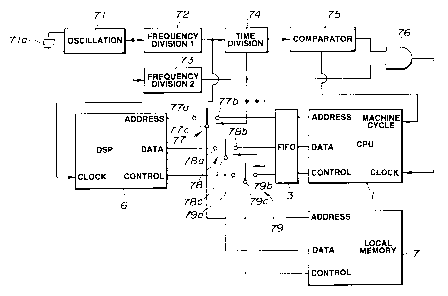
In the synchronization circuit, shown in Fig.2, frequency
signals from an oscillator 71 connected to a quartz oscillator
?la are supplied to a first frequency divider 72 and a second
frequency divider 73. The frequency divider 72 divides the
frequency signals in a pre-set manner to produce DSP clocks shown
in Fig.3a. These DSP clocks are supplied to clock input
ts:rminals of a time-multiplexing control circuit 74 and the DSP
6.
The time-multiplexing control circuit 74 generates time-
13
2 ~ .4308
divisional signals which go high and low alternately and
repeatedly at an interval of four periods of the DSP clocks, with
the eight periods of the DSP signals corresponding to one period
of the time-divisional signals. These time-divisional signals
are fed to first to third switches 77 to 79 anal to a comparator
75.
The second frequency divider 73 has its frequency dividing
ratio set to four times that of the first frequency divider 72.
By dividing the frequency signal from the oscillator 71 with this
frequency dividing ratio, CPU clocks having the frequency equal
to one-fourth the frequency of the DSP clocks outputted from the
first frequency divider 72, as shown in Fig.3C, are generated,
and routes via an AND gate 76 to the CPU 1.
Based upon the CPU clocks, the CPU 1 generates machine cycle
signals changed in synchronization with the time-multiplexed
signals shown in Fig.3b, as shown in Fig.3d, and routes the
machine cycle signals to the comparator 75.
The comparator 75 compares the phase of the time-multiplexed
control signal from the time-divisional signal from the time
multiplexing control circuit 74 and the machine cycle signal from
tie CPU 1. If the two signals are in phase with each other, a
high-level coincidence detection signal is fed to the AND gate
73. If otherwise, a low-level coincidence detection signal is
supplied to the AND gate 76. When fed with the high-level
coincidence detection signal, the AND gate routes a CPU clock
from the second frequency divider 73 to the clock input terminal
o:f the CPU 1. However, when fed with the low-level coincidence
dE~tection signal, the AND gate gates the clock from the second
14
a134~08
frequency divider 73.
Consequently, when the two signals are :not in phase with
each other, the CPU clock which should be fed to the CPU 1 is
gated by the AND gate ?6 and ceases to be supplied to the CPU 1,
:such that the machine cycle of the CPU 1 is shafted a half cycle
t:o assume a normal state.
Thus the synchronization circuit controls the memory
accessing so that memory accessing by the CPU 1 occurs once for
t,wo memory accessing operations performed by the DSP 6.
Specifically, the accessing time of the local memory 7 is
about 330 nsec, that of the DSP is about 240 nsec, each machine
cycle of the CPU 1 is about 1 use and the meme~ry access time of
the CPU 1 is about 375 nsec within the machine: cycle of the CPU
1.
Assuming that the DSP clocks supplied to the DSP 6 by the
synchronization circuit, the CPU clocks supplied to the CPU 1
and the time-multiplexed signal outputted from the time-
multiplexing control circuit 74 are produced. under a regular
condition as shown in Figs.4a to 4c, the memory accessing time
period Mc of the CPU 1 is set in the latter half of each machine
cycle S, as shown in Fig.4d, while two memory accessing time
periods MD1, MD2 of the DSP 6 are set in the former half of the
machine cycle S, as shown in Fig.4e.
On the other hand, the accessing time of the local memory
7 is about 330 nsec, so that three accesses MD1., MD2 and MD3 are
set at an equal interval in each machine cycle S, as shown in
Fig.4g.
Thus an offset is produced in the accessing time of the
213~~08
:Local memory ?, DSP 6 and the CPU 1. Such offset in the
accessing time is adjusted by switching control of the first to
third switches 77 to 79 by the time-multiplexing control circuit
'74 shown in Fig.2 and sound source data writing and readout via
i:he FIFO 3.
That is, the time-multiplexing control circuit 74 generates
changeover control signals shown in Fig.4f, based on the time-
multiplexed signal shown in Fig.4c, and routes the time-
multiplexed control signal to the first to third switches 7? to
~~9. Thus the first to third switches 77 to 7;3 are changed over
1:o select the fixed terminals 7?a to ?9a by movable contacts 77c
1:o 79c during the periods of the first access :MD1 and the second
access MD2 of the local memory 7, while being changed over to
select the fixed terminals 77b to ?9b by the movable contacts 77c
t;o 79c during the period of the third access MC, as shown in
Fig.4g.
Thus the sound source data of the address bus line, data bus
Line and the control bus line of the local memory 7 are fetched
i.n the DSP 6 during the first access period MfDl and the second
e.ccess period MD2 of the DSP 6.
On the other hand, the sound source data of the address bus
line, data bus line and the control bus line :;toyed in the FIFO
3 are routed to the local memory 7 during the access period MC
of the CPU 1.
Thus , with the speech information processor of the present
embodiment, the local memory 7 is employed time-d:ivisionally in
common by the DSP 6 and the CPU 1. TlZis improves the
exploitation efficiency of the local memory '7 arid enables the
16
213~4~08
local memory ? of a smaller storage capacity to be produced
inexpensively, thereby lowering the production cost.
The local memory ? stores the sound source data under the
numbers of, for example, 0 to 255. The sound .source data having
a. non-interval portion (formant portion shown i:n Fig.9) is stored
under numbers different from those for the interval portion
(repetitive portion shown in Fig.9). The sound source data is
read out by eight sound source selection data SRCa to SRCh from
the DSP 6. The sound source data read out by the eight sound
source selection data SRCa to SRCh are routed to signal
processors 20A to 20H shown in Fig. 1.
If the sound source data, stored in the local memory by
being divided into the non-interval portion and the interval
portions, are read out, the non-interval portion of the sound
source data is routed to the signal processor 20A, while the
interval portions of the sound source data are routed to the
signal processors 20B to 20H. The DSP 6 executes the above
processing by software program control. This is explained for
convenience by referring to the functional block diagrams shown
i:n Figs . 5 and 6 .
The DSP 6 processes the eight sound source data (voice data)
A to H time-divisionally for forming and outputting two channels
(:Left and right channels) . Specifically, the sampling frequency
o:f the DSP 6 is set to 44.1 Khz, such that a sum total of 128
c;~rcles of the processing operations, with each cycle being 1?0
nsec, is performed for eight sound source data and two channels
within each sampling period (1/ fs).
That is, the sound source data fed to the ;signal processors
1?
~' 134308
20A to 20H are supplied to switches SIa to aIh. Each of the
switches Sia to Sih is fed from a register RAM in the DSP 6 with
control data KON designating the start (~cey-on) of sound
production of each sound source data, or with. control data KOF
designating the cessation (key-off) of sound production of each
sound source data, via terminals 31a to 31h, so as to be thereby
turned on and off.
Each of the control data is made up of eight bits of data
DO to D7, these data DO to D7 being associated with key-on and
key-off of the sound source data A to H. These control data are
written in separate registers.
Thus it suffices for the user to set a flag "1" for the
sound source data desired to be keyed on or off, so that the
laborious operation of preparing a program in which a bit not
changed for each sound note is temporarily written in the buffer
register may be eliminated.
The sound source data via the switches S:ia to Sih are fed
to a data expansion circuit 21 provided in each of the signal
processors 20A to 20H. Since the sound source data are
compressed from 16 bits t;o 4 bits and stored in, this form in the
sound source RAM, the data expansion circuit 21 expands the sound
source data compressed to 4 bits to generate 16-bit sound source
data which is supplied vi.a a buffer RAM 22 to a pitch conversion
circuit 23.
The pitch conversion circuit 23 is fed with pitch control
data P(H) and P(L), such as processing parameters, from the
register RAM via a terminal 33a and a control circuit 24. Thus
tile pitch conversion circuit 23 interpolates :Forward side four
18
2134308
:samples and rear side four samples by over-sampling based upon
t;he pitch control data P(H) and P(L) in order to perform pitch
conversion with the same sampling frequency fs as that for the
input sound source data.
If lower bits of the control data P(L) are set to 0, it
becomes possible to prevent the interpolating data from being
non-uniformly thinned out and hence to prevent fine pitch
wobbling in order to produce the high-quality playback sound.
The switch S2a is adapted for being turned on and off by the
control data FMON (FM-on) supplied from the register RAM via a
terminal 35a. When the switch 2a is turned .on by the control
data FMON, sound source data such as the sound source data H is
fed to the control circuit 24. When fed with such other sound
source data, the control circuit 24 substitutes the sound source
data for the pitch control data P(H) and ~?(L) in order to
transmit the sound source data to the pitch conversion circuit
23.
Thus the sound source data A is frequency-modulated in the
pitch conversion circuit 23, such that, if the modulating signal
is of an extremely low frequency of several Hz, vibrato is
applied to the modulated signal, whereas, if the modulating
signal is of a variable frequency, the sound tone of the playback
sound of the modulated signal may be variegated, so that it
becomes unnecessary to provide a special sound source for
modulation and the FM sound source can be produced by the sampler
system.
The control data FMON is written in an eight-bit register,
as is the control data KON, such that the data DO to D7 of
19
213.308
respective bits correspond to the sound source data A to H,
respectively.
The sound source data via the pitch conversion circuit 23
are supplied to a multiplier 26. The multiplier is also fed via
a terminal 36a, a control circuit 27 and a switch S3a with a
control data ENV for controlling the envelope from the register
FtAM, while being also fed via a terminal 37a, a control circuit
~:8 and a switch S3a with a control data ADSR for ADSR control.
The switch S3a is changed over by the upper most bit (MSB)
of the control data ADSR, such that, if the MfSB of the control
data ADSR is "1", the switch S3a is changed over to select the
control data ADSR from the control circuit 28 (ADSR mode) and,
if the MSB of the control data ADSR is "0" , the switch S3a is
changed over to select the control data ENV from the control
circuit 28 (ENV mode).
When fed with the control data ENV, the multiplier 26
processes sound source data from the pitch conversion circuit 23
with envelope control such as fading. As for such envelope
control, one of five modes, that is direct designation, linear
fade-in, kinked line fade-in, linear fade-out and exponential
fade-out, may be selected by the upper three bats of the control
data ENV. The current wave crest value is adopted as the
initial value of each made.
It is noted that, if the sound source is a drum or a piano,
the total sound production period is divided into an attack
domain, a decay domain, sustain domain and a release domain, and
the signal amplitude exhibits peculiar change state in each
domain. Thus, when fed with the control data ADSR, the
213~3(~8
multiplier 26 performs a control operation of correspondingly
changing the level of the sound source data of each voice on the
sound source data from the pitch conversion circuit 23.
Specifically, with such control operation, the signal level
is raised linearly only during the attack domain, while it is
lowered exponentially during the three domains of decay, sustain
and release. The time duration of the fade-in and fade-out is
suitably set for each mode depending on parameter values
specified by upper five bits of the control data ENV.
The time duration of the attack and susta5.n is suitably set
depending on parameter values specified by upper and lower four
bits of the control data ADSR, while the sustain level and the
time duration of the decay and release is set depending on
parameter values specified by each two bits of the control data
ADSR.
With the present DSP 6, the signal level is raised linearly
only for the attack period during the ADSR mode for decreasing
t:he number of times of 'the arithmetic-logical operations. By
switching the ADSR mode to the ENV mode, setting the attack
domain to the kinked line fade-in and setting the three domains
of decay, sustain and release to exponential fade-out, it is
possible to manually perform spontaneous ADSR control operations.
By supplying output sound source data of the multiplier 26
v:ia a terminal 41a to the register RAM and supplying the control
data ENV via a terminal 42a to the register RAM for rewriting for
e<~.ch sample period, it becomes possible to produce speech signals
of arbitrary envelope characteristics having significantly
different pitches from the sound source data of the same musical
21
instrument . L ~ .~
If the noise is employed as the effect sound, the noise data
from an M-series noise generator, not shown, ins supplied to the
multiplier 26 in lieu of the sound source data from the pitch
converter 23.
The sound source data from the multiplier 26 is fed to
second and third multipliers 291, 29r. The second multiplier 291
is fed with left sound volume control data LVL for controlling
the left channel sound volume from the register RAM via a
terminal 38a, while the third multiplier 29r is fed with right
sound volume control data RVL for controlling the right channel
s~~und volume from the register RAM via a terminal 39a.
The second multiplier 291 multiplies the sound source data
with the left sound volume control data LVL for producing left
channel sound source data having a pre-set sound volume and
outputting the produced data via a terminal TLa. The third
multiplier 29r multiplies the sound source dai~a with the right
sound volume control data RVL for producing right channel sound
source data having a pre-set sound volume anal outputting the
produced data via a terminal TRa.
Figs.? and 8 show maps for all of the control data on the
register RAM.
Thus the left channel sound source data, generated by the
signal processing units 20A to 20H, are supplied via terminals
Tla to TLh shown in Fig.6 to a left channel signal processing
unit 50L, while the right channel sound source data are supplied
vi.a terminals Tra to TRh to a right channel ;signal processing
unit 50R.
22
213408
In the left channel signal processing unit 50L, the sounc
source data supplied via the terminals Tla to Tlh are fed to
main additive unit 51m1, while being fed via switches S4a to S4r
to a subsidiary additive unit 51e1.
In the right channel signal processing unit 50R, the sounc
,source data supplied via the terminals Tra to Trh are fed to
main additive unit 5lmr, while being fed via switches S5a to S5r
to a subsidiary additive unit 5ler.
The additive units 51m1, 5lmr add the sound source date
supplied thereto via the terminals TL a to Tlh and Tra to Trh tc
supply the resulting sums to a multiplier 52.
The multiplier 52 is fed from the register RAM via a
terminal 62 with control. data MVL for controlling the main sound
volume. The multiplier 52 multiplies the sound source data with
':.he control data MVL- to control the main sound volume of the
;pound source data and transmits the resulting product to an
additive unit 53.
To the switches S4a to S4h and S5a to S5h of the signal
processors 50L, 50R are routed control data EONa to EONh for
adding the echo (reverberating sound) from the register RAM via
terminals 61a to 61h. The sound source data (voice) to be added
t.o with the echo is selected by these control data EONa to EONh.
When the signal processing of the non-interval component is
performed by the signal processing unit 20A for the voice A, the
switches S4a and S5a are controlled so as to be turned off so
that no echo is added to the non-interval portion.
The control data EON is written in an 8-bit register, as
shown in Fig.8.
23
214308
The subsidiary additive nodes 51e1, 5ler add the sound
source data supplied via the switches S4a to S4h and S5a to S5h
a.nd transmit the resulting sum data to channel echo control units
14E1, l4Rr via an additive unit 54.
The echo control units 14E1, l4Er are fed via a terminal 64
with control data EDL (echo delay) for controlling the amount of
the echo and control data ESA (echo start address) indicating the
sound source data to be added to with echo. The echo control
units 14EL, l4Er add echo to the sound source data from the
subsidiary additive units 51e1, 5ler within the range of 255 msec
so that the left channel echo and the right channel echo will be
equal to each other, and transmits the resulting data via a
buffer RAM 55 to a digital low-pass filter, such as an infinite
impulse response (FIR) filter 56.
The FIR filter 56 is fed from the register RAM via a
terminal 66 with 8-bit coefficients CO to C'7, added to with
codes, and has its filter characteristics variably controlled so
that the echo sound will be produced which i.s spontaneous in
psychoacoustic effects. The sound source data via the FIR filter
56 is supplied to multipliers 57, 58.
The multiplier 57 is supplied with control data EFB (echo
feedback) from the register RAM via a terminal 57. The
multiplier 57 multiplies the sound source data from the FIR
filter 56 with the control data EFB and rouges the resulting
product to the additive unit 54. The additive unit 54 adds the
sound source data from the subsidiary additive units 51e1 and
5lEr to the sound source data from the multiplier 57z and routes
t:he resulting sum to the echo control units 14E1 and l4Er.
24
2134~Q8
The multiplier 58 is fed with the control data EVL for
controlling the amount of the echo sound from the register RAM
via a terminal 68. The multiplier 58 multiplies the sound source
from the FIR filter 56 by the control data EVL to adjust the
sound volume of the echo in the sound source d<~ta and routes the
resulting product to the additive unit 53.
The additive unit 53 sums the sound source data from the
main additive units 51m1 and 5lmr to the sound. source data from
the multiplier 58 to add the echo to the sound. source data from
the multiplier 5lmr, and outputs the resulting; sum via an over-
sampling filter 59 and a left-channel sound source data output
terminal Lout and a right-channel sound source terminal Rout,
respectively.
The sound source data outputted from the DSP 6 via output
terminals Lout, Rout are fed to the D/A converter 8 shown in
Fig. 1. The D/A converter 8 converts the sound source data into
analog signals to form speech signals which are supplied to the
speaker unit 9. Thus the speech corresponding to the sound
source data is produced by the speaker unit 9.
The control data MVL for controlling the main sound volume
and the control data for controlling the echo sound volume are
8-bit data devoid of codes and are independent of each other and
with respect to the left and right channels.. Thus the main
speech signal and the echo signal may be adjusted in level
independently of each other to render the speech produced by the
speaker unit 9 sufficient in ambience.
In the above description, the sound source data read out
from the sound source ROM of the host computer system 10 is
CA 02134308 2003-10-09
written in the FIFO 3 under control by the CPU 1. However, a
direct memory access controller (DMAC) 11 may also be provided
as shown by a broken line in Fig.1 for transferring the sound
source data read out from the sound source ROM to the FIFO 3.
Since the DMAC 11 is a hardware designed for use exclusively
for data transfer, the sound source data may be transferred
without the interposition of the CPU 1, so that faster data
transfer may be achieved than is possible with the CPU 1.
In additior_, in the above description, the local memory 7
has a storage capacity of 64 kbytes, and the memory access time
is 330 nsec. However, these numerical values are merely
illustrative and are not limitative of the present invention.
Thus the present invention is not limited to the numerical values
given herein and may be modified in a desired manner without
departing from the scope of the invention.
26