Note: Descriptions are shown in the official language in which they were submitted.
~3~3~~
w~ 9an~o~ PCTms94~oxoss
EL,ECTI2C~LUl~II~IESCEhIT DISPLAY
VVIThI BRIGHTNESS ENHANCEMENT
Background of the Invention
A wide ~r~riety of illuminated electronic displays are currently in
common use. Perhaps the most familiar of such displays are cathode ray
tubes
~CI~T's). CRT's are popular because they have many advantages. They
produce
14 bright, high resolution, color images. They do, - however, have
significant
,
disadvantages ire certain situations. ' Compared with alternatives such
as liquid
crystal displays (LCD's) and electroluminescent displays {ELD's) they
ire bullry
and consume l~.tge quantities of power. In contrast; LCD's are anuch
thinner and
consume much less power. This makes LCD's preferable for applications
where
15 space or energy consumption is important. Examples of applications
where
such
considerations axe important are lap-top computers, vsrhere both energy
consumption and 'sgace are critical, and automobile dashboard displays;
where the
volume is bf particular imp~oLtance.
Because L,CD's are 'not light emitting, they require a light source.
24- Although they may use ambient light, an internal light source
typically
placed
behind the display usually provides greater readability, ,especially
in a dark
env'ironm~nt. As a result, there is a minimum thickness necessitated
by the
~lumination source.
An alternative' type of 'display is electroluminescent. In an
25 electroluminescer~t display, electroluminescent materials may be
used
as a light
source for another type of display, such as an LCI~, or may be both
the light
a
'source and the display itself. Ele~troluminescent displays have the
advantage of
being thin, cool, ~d highly efficient, dJne problem with eleGtroluminescent
d
displays, however, is a lack of brightnesso This is often overcome by
increasing
34 the voltage applied to thd ele;~troluminescent material. While
this
will increase the
brightness of the display, it reduces the display's reliability and
lifetime.
CA 02134356 2005-07-04
60557-4861
-2-
A second problem with electroluminescent displays
is that they are inherently grainy in appearance. This
graininess reduces readability and increases operator
fatigue especially when such displays are used for extended
periods of time. The increase of voltage that will produce
brighter intensity still does little or nothing to overcome
the problem of the grainy appearance.
Summary of the Invention
According to the present invention there is
provided a backlit display comprising: a case having an
optical window and an axis normal to said optical window; an
electroluminescent panel in said case; a structured surface
material between said electroluminescent panel and said
optical window, said structured surface material having the
property that light entering it while making an angle in a
first predetermined group of angles with said axis will be
reflected and light entering it while making an angle in a
second predetermined group of angles with said axis will be
refracted such that the majority of the light in said second
group of angles will form an output wedge that is narrower
than its associated input wedge, said angles in said second
group of angles being greater than said angles in said first
group of angles; a,nd a light gating device between said
structured surface material and said optical window.
The invention provides the expected result of
increasing the apparent on-axis brightness of the display
but also provides the unexpected result of alleviating the
inherent graininess of the electroluminescent light sources.
Brief Description of the Drawinqs
Figure 1 shows a first embodiment of the
invention;
CA 02134356 2005-07-04
60557-4861
-2a-
Figure 2 shows the operation of the structured
surface material used in the invention;
Figure 3 is a graph of the operation of the
structured surface material used in the invention;
Figure 4 shows the construction of an
electroluminescent panel that may be used in the invention;
and
Figure 5 shows a second embodiment of the
invention.
W~ 9a121094 ~ t~ ~ ~ ' PcTTrcJS9a~ozoss
~:.y.. ,.t
-3-
Detailed Description
of the Preferred Embodiments
The present invention relies on the lmown phenomenon that certain
types of structured surface materials will, when accepting light from a
lambertian,
~ area source, increase the apparent on-axis brightness of the source by
reducing the
size of the wedge ~f emitted light> It has been found that when such
a source is
used in conjunction with an electroluminescent light source, it has
the unexpected
result ~f also significantly reducing, car even eliminating the graininess
normally
inherent in an electzoluminescent light source.
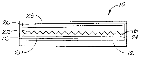
Figure 1 illustrates a first embodiment of a display, 10, according
to the invention. hisplay 10 includes a case 12. , Display 10 includes
an
electroluminescent panel 16 and a structured surface material 18.
Electroluminescent panel l6 includes an electroluminescent material
and a reflector
behind the electroluminescent material. The reflective material, in
this
embodiment, is preferably a diffuse reflector. )Jlectroluminescent
panel 16 is
described in more detail below.
Structured surface material 1 ~ has a smooth surface 20 and a
structured surface 22~ Smooth sc~rface 20 lies toward the back of display
lfl and
structured surface 22 lies toward the front. To insure that 'they are
not optically
coupled, :electroluminescet~t panel i6 and structured surface material
18 are
preferably separated by a small air gap 24. Structured surface material
18 and its
operation': in the invention will be described in greater detail in
conjunction with
Figures 2 and 3.
Display 10 further includes a light gating device 26: Typically light
gating device 26 is a' 3iquid crystal display: As is well known in
the art, a liquid
crystal display inay' be made transparent or opaque; in the case of
a monoc$rome
display, or transparent or a variety of colors in the case of a color
display by the
proper application of el~trical signals. This will form images that
will be visible _:
when electrolunninescent display is, illuminated. Display 10 further
includes a
transparent cover sheet 2$:'
W w A..w.~?r~.:..
. ., r .._
~p<- xr .
..
."~-~ . ~2
r."
r..
H 7~t8~..
- "T.F L..
.
.,(4 4. N'o-.,
i." .r c
";.
'."'
a n b . :3
,: re . ~.
m 3 ....
v~ e.rr..
..~., r ..,t.r.
..q,.....
i2 .. . .,t-7
' . Fo..
Y "'. .'a
Y
,.,:.x,- o.
.,
k
. 1 .f.
tr .
' _ ;.. ..,.."t
. f . 1.,:~:.
r:w-
,Zd::
w. 1
r l, ~ .,?
a JY ...,.,)
:..
?s .. , ~
,'.f.~
.~ .im.?;,>.
> ., . ...
. <.,.. ...
. , ... .
.. , ..,....
,1.~~_.......
., . . ,
.....r.....v,.,.,...
, ., ..,
. r..,.rr...v....>..,.~..
.... o.,
.".......
.... ." ,
,. . ~ ,.
. , ,.,.
... t.. -
. , .. .
.
WO 9412109 ~ IsCZ'/US94/02058
_ 1~'a;
4 .,
Figure 2 is anenlargement of structured surface material 18 of
Figure 1. As described previously, structured surface material 18 has a smooth
side 20 and a structured side 22. Structured side 22, in the preferred
embodiment, ,
includes a plurality of triangular prisms. In the preferred embodiment, such
prisms are right ISOSCeIeS priSIllS, although prisms having peak angles in
tlae range .
of 70 degrees to 110 degrees will work with varying degrees of effectiveness
with
the invention. Structured surface material 18 may be of any transparent
material
having an index of refradtion greater than that of air, but, in general, the
materials
with higher indices pf refraction will produce better results. Polycarbonate,
which .
has an index of refraction of 1.586; has proven to work very effectively. For
purposes of description of the invention, the prisms on structured surface 22
will
be assumed to have included angles of 90 degrees and structured surface
material
18 will be assumed to be of polycarbonate. Alternatively other structured
surface
materials may be used. Symmetric cube comer sheeting has been shown to
produce excellent results.
Figure 3 illustrates the operation of structured surface material 18.
Figure 3 is a graph having two axes 26 and 28. These axes represent the angle
that a light ray makes to a normal to smooth surface 20. Specifically, axis 26
represents the angle that the light ray makes when tie direction of the light
ray is
projected into a plane parallel to the linear extent of the structures on
structured .
surface 22: Similarly axis 28 represents the angle that the light ray makes to
a
normal to smooth surface 20 when the direction of the light ray is projected
into
a plane perpendicular to the linear extent of the structures on structured
surface 22.
Thus a light ray strikiing perpendidular to smooth surface 20 would be
represented
by the origin, labeled 0 degrees, of the graph of Figure 3. As may be seen,
'Figure 3 is divided into a~egions 30, 32; and 34. Light striking at angles
that fall
within region 30 will enter structured surface material 18 but be totally
internally
reflected by structured surface 22 so that they pass through smooth surface 20
a
second time and reenter air gap 24. Light rays striking smooth surface 20 at
an
angle such that they fall in region 32 or 34 will be transmitted but refracted
to a '
l
3
5, ..:~-'.:'. '.. -.. . .," :. ~;..~. . ~ ': .; '; , ..~y.:~ .:,.... n r,..
;,.,... ,-..'.'. '...~';:.: , '.'.;:.., , ','.;. , W ~:,; -.~::~... . : ,::.
~.. . .,.
s
PC:T/US94/02058
. .~. ~0 94!21094 ~ ~ ~ L~ ~ ~ ,i a
f '.:;
-5-
different angle with respect to the normal. As may be seen from Figure 3,
which
1 represents the performance of polycarbonate, any light ray striking smooth
surface
2Q at an angle of less than 9.4 degrees to the normal, will be reflected.
Returning to Figure 2, four exemplary light rays are shown. The
first, light ray 36, approaches smooth surface 20 at a grazing angle, i.e., an
angle
to the normal approaching 90 degrees: If light ray 36 makes an angle of 89.9
degrees to the normal t~ surface 20 when it strikes structured surface
material 18,
it vmrill be refracted such that it snakes an angle of 39:1 degrees to the
normal as
it travels through structuresi surface I'naterial 18.; Upon reaching
structured surface
22; it will be r~fxaeted again. Because of the structures on structured
surface 22,
- it ~,vill be refracted so that again it will nnake a smaller angle to the
normal to
stnactured surface 20: In the exarziple it will make an angle of 35.6 degrees.
Light ray 38 approaches smooth surface 20 at an angle much closer
to the cut off angle. ' It also is refracted as it passes through smootlh
surface 20,
1~ but to a lesser extent: If light ray 38 approaches smooth surface 20 at an
angle of
10 degrees to the normal to smooth surface 20; it will emerge from structured
' surface 22 at an angle of 37:7 depress tci the normal to smooth surface 20
but on
the n site side of that normal.
Light ray 40 approaches at an angle~less than the cut off angle and
is totally internally reflected twice by structured surface 22 and returned to
the
interior of display 10:
Finally; light ray 42 approaches smooth surface 20 at an angle
similar to that c~f light ray 38, but in a location such that it is totally
internally
reflected by one side flf a prism on structured surface 22 but not by the
second
side: As a resdlt it emerges at a large angle to the normal to smooth surface
20.
' l~cause such a geflection only occurs to a light ray' that is travelling in
a direction
that forms a high incidence angle to the side it strikes, the prisms provide a
very
,,,
small cross section t~ such rays. In addition many of those rays will reenter
the
next prism and be returned into display 10.
''6~0 94/2094 ~ ~ ~TIIJS94/0205~
~''-,; I
. ~ . .
..$_
A fifth class of light ray is not shown in Figure 2. This is the set
of light rays that are reflected by smooth surface 20 and do not enter
structured
surface material 18. Such light rays simply join the others that are reflected
back
into display 10.
As may be seen from this discussion, light that, absent structured
surface material 18, would have emerged from the display at a high angle to
the
axis of the display; sarhere the axis of the display is taken to be the normal
to
smooth surface 20, is redirected into a direction closer to that axis. A small
amount of light will be directed out at a large angle to the axis. Thus, we
may say .
that Light that enters structured surface material 18 through smooth surface
20 with
an angle of incidence greater than a predetermined angle is directed into an
output
wedge that is narrower than the input wedge and the majority of the light that
enters structured surface material 18 through smooth surface 20 at an angle of
incidence of less than that predetermined angle will be reflected back into
display
10.
The fight that is reflected back into display 10 will strike
eleetroluminescent panel 16. In general, most of the light that strikes
electroluminescent panel 16 will be diffusely reflected either by the
electroluminescent material itself or by the reflector~behind it. Then it will
travel
back to structured surface material 18, in general making a different angle
than it
made the first time. The process is then repeated so that more of the light is
redirected into the smaller wedge. The key aspect of the invention is that
structured surface material 18 must be capable of reflecting light striking it
in a
farst predetermined group of angles and passing, but refracting, light
striking it in
2S a second predetermined group of angles wherein the angles in the second
group of
'au~les are greater than' those in the first group of angles and wherein the
light in
the second group of angles is refracted into an output wedge that is narrower
than
its input wedge. ;
Figure 4 is an exploded view of an electroluminescent panel that
could be used with the present invention. Such electroluminescent panels are
available from Durel Corporation under the trade name I3ure1 3. The
~~ 941x1094 ~~ ~ e~? ~ ~ ~ ~ :~'~T'/~JS94102a58 .
~::_; ,, .a
_7_
electroluminescent panel ef Figure 4 includes a transparent fzont insulator 50
that
provides electrical insulatian and protection to the electroluminescent
system.
Front insulator 50 may be, for example, of polyester. An electrically
conductive
material, 52, is applied to one surface of front insulator 50. Electrically
conductive layer 52 is preferably made very thin so as to be essentially
transparent. Beneath electrically corxductive layer 52 is the
electroluminescent
material 54. Underlying electroluminescent material 54 is a dielectric layer
56.
dielectric layer 56 acts as the reflector behind the electroluminescent
material as
discusse~t previausly: Dielectric Iayer 56 is preferably a diffuse reflector.
Underlying dielectric material 56 is rear electrode S8. Finally, rear
insulator 60
provides electrical insulation and physical protection to the rear of the
electroluminescent panel.
Figure 5 illustrates a second embodiment of the invention. ' The
embodiment of Figure 5 is essentially the same as that of Figure 4 with two
: madi~cations: The first modification is the addition of a second structured
surface
film; 18' : Structured surface film 18' is typically identical to structured
film 18
except that the structures run: perpendicular to those of film 18. The second
change is the addition of a diffuser 62: lay including a diffuser 62 it is
possible
to snake reflector 56 of Figure 4 a specular reflector inst~d of a diffuse
reflector.
Diffuser 62 then provides the -randomization of the direction of tine light
making
~SSible the function of the invention.
l l
,3
w ~ .,. . ., ,'l;.
S' n
. . J
~ .~ \.