Note: Descriptions are shown in the official language in which they were submitted.
CA 02134369 2003-07-25
1
DIGITAL TELEVISION SYSTEM
CROSS REFERENCE TO RELATED PATENTS
The following I:~atents are related to the present
application.
U.S. Patent No. 4, 67.5, 595, entit:Led,
~~FRAME ADDRESSED SPATIAL LIGHT MODULATOR" and issued
October 7, 199E>;
U.S. Patent No. 5,079,544, ent=itled,
~~STANDARD INDEI~ENDENT DIGiTIZEh V:LDE:O SYSTEM" and issued
January 7, 199a?; and
U.S. Patent No. 4,939,575 ent=itled,
~~FAULT-TOL:ERAN~L' SERIAL VIDEO PROCESSOR DEVICE;" and issued
July 3, 1990.
TECHNICAL FIELI:~ OF THE INVENT7:ON
This invention relates in general to the field of
electronic devvwces. Mc:>re particularly, this :Lnvention
relates to a digi.ta~. t:.el.evision system.
2134369
2
BACKGROUND OF THE INVENTION
Standard television has not kept up with the modern
electronic revolution as exemplified by the recent
developments in the personal computer industry.
Consequently, a standard television system does not
produce as high a quality picture as one might expect
given the recent advancements seen in other modern
electronic systems.
Standard television systems may receive and display
l0 analog, rather than digital, video signals. A typical
standard video signal is referred to as an "interlaced"
video signal. This means that each frame of video data
displayed on the standard system is divided into two
fields. The first field may, for example, contain the
odd lines of the video frame. The second field may
contain the even lines of the same video frame. The two
fields making up the single frame are received and
displayed successively on the standard system and may
appear to a viewer as a single frame. Dividing and
displaying a video frame in this manner may decrease the
quality of the output of a video system.
Additionally, a standard television system may
include an analog display such as a cathode ray tube
(hereinafter "CRT"). Because a CRT is an analog device
that does not provide a linear response to an input
signal, a "gamma curve" is introduced into a standard
video signal to compensate for the non-linearity of the
CRT. Standard video signals therefore are not directly
compatible with a linear digital display.
Furthermore, a standard television system may not be
operable to process a video signal prior to displaying
the video signal. Similarly, a standard television
system may not be programmable to operate on a number of
different standard video signals. Finally, a standard
2134369
3
television system may be limited to a small display area
on the order of 640 by 480 pixels.
CA 02134369 2003-07-25
4
SU1~1ARY OF THE INVENTION
In accordance witE~; the preserut invE>nt.ion, a digital
television system is provided which substantially
eliminates or rE_rduces cl-:.sadvantages and prc>blems associated
with prior systems. Phe~ teachings ofthe ~>resent invention
provide a digital telev:~:~ion sy:~tem that processes video
signals in a parallel architect=ure. A parallel
architecture ha.. not bean previc:usly used i.n a television
system.
More ~;pecifical:ly, the present invention provides a
digital television system that rnay process input video
signals in varicnus form::. The ~~ys~em comprises dividing
circuitry that i.s operak>l.e to dwvicie a line of input video
signals into a ~nlurali.ty of channels fcr each input video
signal. The ch<~.nnels of: input video signals are processed
in parallel. Ttue pro~;essed video ~>ignals may be displayed
on a display.
In accordance wi t.h one aspects of the present: invention
there is provide d a digital television system, comprising:
dividing circuit=.ry operable to ciiv:ide a l..ine of input video
signals into a ~_~lural..t~jr of channels fcr each input video
signal; processing circ.;ai.try re:>porrsive too sa~_d dividing
ci~__°cuitry and operab 1 :.e t:c> simul t:aneously process said
channels of inpl<t video signals to produce processed input:
video signals; and displaying c_rcuitry responsive to said
processing circuitry and operab~~e t o disp:La.y said processed
input video signals.
It is a technical advantage of the present invention
to provide a digital t:~.~levision sy::7terrr that. processes a
video signal in a plurality of parallel channels. 'rhe
CA 02134369 2003-07-25
channels of the system rnay correspond to vertical strips of
a video frame. Each :hannel may contain an overlap of, fc>r
example, one to five ~i~;els with an adjacent channel. The
overlap between chann~=.1s may allow identical horizontal
5 processing of pixels ~.~rz the ends of: each channel. The
overlapping pixels may ioe removed before the processed
video signal is displayE-ed such that redundant pixels are
not: displayed.
It is another tec:hn:ical advantage of t=he present
invention to provide ~-~ digital t:elevisiorr system that is
operable to convert a standard video signal into a
non-interlaced video ~icr;al. The system may convert each
fie.Ld of an interlace~i video si_c~nal_ into a non---interlaced
frame. Additionally, tle system may remove the effect of a
standard gamma curve from a stanc~lard video signal.
It is another technical advantage of the present
invention to provide a r_li.gital television system including
a digital display sacra ,:s a spat:ia~~ light: modusLator. The
di:~play may provide 2' intensity levels i.n :response to X bit
planes formed for eacr~ of the video signals from video data
for each pi:~el in a vicaeo frame. i'he first bit plane for
each input ;rideo signa:L, corres~>onding to the rnost:
significant bit for eacaa pixel, may control the display for
one-half of the time rc>r one frame. Successivre bi.t planes.
may each contro7_ the c.;i:;~:lay for a period of t.irrle
proportionate to the po>.ition c>f the bits of that bit plane
in the pixe:Ls making ~.~p that bi.t. pi.ane.
It is a techni.ca.l.~sdvantage of the present. invention
to provide a programmal:oie digital television ~;ystem. The
system may be px:ogramrnec.l by a user to process a particular
standard video :signal. Ad.ditionall.y, the system may be
CA 02134369 2003-07-25
5a
programmed to implement various functions to produce a high
definition display from a standard video signa:i input.
It is another technical advantage of the present
invention to prcvide ,~ ck.i.gital television system that is
operable to process zved, green and blue video signals or a
luminance video signal. ~=cr~.d two c~~lc>r difference video
signals.
It is another te~chnic:al advarntage of the present
invention to provide :a digital t:elevi.sion systa=_m that is
operable to modify tht> w>ize of a video frame. The system
may expand the pixel ~~r:iclth of a videc> frame by controlling
the rate at which a l:i_nE> of video data is sampled.
Additionally, tk~e syst:em may scale the number caf lines in a
video frame.
In accordance with another aspect of the present
invention there is pr~rvided a h~_gh definition digital
television system, ca:nprising: receiving c:irc~aitry
operable to receive a video signal and to provide a
plurality of digital videa signals; dividing circuitry
responsive to s<~.id receiving c~.rcuitry and operab'~e to
divide a line of wick dickital. v~,~eo signals, into a
plurality of channels for:v each digital. video signal;
processing circlaitry responsive to sai.c~ dividing circuitry
and operable to simultaneously process said channels of
digital video s:i.gnals; ~rnd a display device responsive to
said processing circuitry and oi:erable to display said
processed digital video signals.
It is another tE.c:hnical ad~aantage of 'the present
invention to provide <:~ ,:iigital t~elevisi.on ~syst.em with a
large display ax:ea an the order of 2098 by 1152 pixels.
2134369
6
BRIEF DESCRIPTION OF THE DRAWINGS
For a more complete understanding of the present
invention and the advantages thereof, reference is now
made to the following description taken in conjunction
with the accompanying drawings in which like reference
numbers indicate like features and wherein:
FIGURE 1 illustrates a digital television system
constructed according to the teachings of the present
invention;
FIGURE 2 illustrates four vertical strips created by
the system of FIGURE 1;
FIGURE 3 illustrates the overlap in pixels between
adjacent channels created by the system of FIGURE 1;
FIGURE 4 illustrates an embodiment of the composite
video interface and separation circuit of FIGURE 1
constructed according to the teaching of the present
invention;
FIGURE 5 illustrates an embodiment of the analog to
digital converter circuit of FIGURE 1 constructed
according to the teachings of the present invention;
FIGURE 6 illustrates an embodiment of the line
slicer of FIGURE 1 constructed according to the teaching
of the present invention;
FIGURE 7 illustrates an embodiment of a channel
signal process of FIGURE 1 constructed according to the
teachings of the present invention;
FIGURE 8 illustrates a gamma correction function
according to the teachings of the present invention;
FIGURE 9 illustrates an embodiment of a processing
module of FIGURE 7 constructed according to the teachings
of the present invention;
FIGURE 10 illustrates another embodiment of a
processing module of FIGURE 7 constructed according to
the teachings of the present invention;
2134369
FIGURE lla illustrates the relationship between the
pixels used by a motion detection function according to
the teachings of the present invention;
FIGURE llb is a flow chart for performing a motion
detection function according to the teachings of the
present invention;
FIGURE 12a illustrates the relationship between the
pixels used by a motion detection function according to
the teachings of the present invention;
FIGURE 12b is a flow chart for performing a motion
detection function according to the teachings of the
present invention;
FIGURE 13a illustrates the relationship between the
pixels used to perform the temporal motion detection
function according to the teachings of the present
invention;
FIGURE 13b is a flow chart for performing temporal
motion detection according to the teachings of the
present invention;
FIGURE 14 is a flow chart for performing spatial
filtering according to the teachings of the present
invention;
FIGURE 15a illustrates a motion adaptive
interpolation function according to the teachings of the
present invention;
FIGURE 15b is a flow chart for performing a motion
adaptive interpolation function according to the
teachings of the present invention;
FIGURE 16 illustrates a line averaging interpolation
function according to the teachings of the present
invention;
FIGURE 17 illustrates a line doubling function
according to the teachings of the present invention;
FIGURE 18 illustrates bilinear interpolation for
scaling three lines of input video signal into four lines
2134369
a
of output video signal according to the teachings of the
present invention;
FIGUREs 19 and 20 illustrate cubic interpolation for
scaling three lines of input video signal to four lines
of output video according to the teachings of the present
invention;
FIGURE 21a through 21d are flow charts illustrating
various methods for performing picture quality functions
according to the teachings of the present invention;
FIGURE 22 is a graph showing the affect of a hue
control input according to the teachings of the present
invention;
FIGURE 23 is a graph showing the affect of a
saturation control input according to the teachings of
the present invention;
FIGURE 24 is a flow chart that illustrates the
operation of a sharpness function according to the
teaching of the present invention;
FIGURE 25 illustrates a configuration of pixels used
in the sharpness function according to the teaching of
the present invention;
FIGURE 26 is a flow chart that illustrates the
operation of a contrast function according to the
teachings of the present invention;
FIGURE 27 is a graph illustrating the effect of the
contrast function according to the teachings of the
present invention;
FIGURE 28 is a graph illustrating the effect of the
brightness function according to the teachings of the
present invention;
FIGURE 29 illustrates an embodiment of a formatter
of FIGURE 1 constructed to the teachings of the present
invention;
2134369
9
FIGURE 30 illustrates an embodiment of a data format
unit of FIGURE 29 constructed according to the teachings
of the present invention; and
FIGURE 31 illustrates an embodiment of a display of
FIGURE 1 constructed according to the teaching of the
present invention.
2134369
5
DETAILED DESCRIPTION OF THE INVENTION
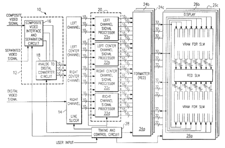
FIGURE 1 illustrates a digital television system
indicated generally at 10 and constructed according to
the teachings of the present invention. System 10
comprises a parallel architecture wherein input video
signals may be divided into channels to be processed in
parallel. For example, system 10 may implement
appropriate functions such that a standard video signal
may be used to provide a high definition video display.
10 Alternatively, system 10 may sample and display a high
definition video signal.
System 10 may receive video signals in composite or
component form. For example, system 10 may receive an
analog composite video signal, an analog video signal in
component form, or a digital video signal. System 10 may
convert a composite video signal into a plurality of
video signals for processing. For example, an analog
composite video signal in the format established by the
National Television Standards Committee (hereinafter
"NTSC") may be separated into a luminance signal,
identified by the symbol Y, and two color difference
signals, identified by the symbols I and Q.
Alternatively, system 10 may separate other standard
composite video signals into appropriate video signals
for processing according to Table 1 below.
TABLE 1
_ .-
~_
Input Video Format Color Space Domain
NTSC y~ I
PAL and SECAM Y, U, V
SMPTE 240M, SMPTE 260M Y, Pr, Pb
It is noted that the other standard video formats
include: Phase Alternating Line, hereinafter "PAL";
2134369
11
Sequential Color with Memory, hereinafter "SECAM"; and
Society of Motion Picture Engineers, hereinafter "SMPTE".
Each of these standard video signals comprise a
luminance signal, hereinafter "luma" or "Y", and a
chrominance signal, hereinafter "chroma" or "C". The
chroma signal may be further divided into appropriate
color difference signals as shown in Table 1. For
clarity, each of the standard video signals may
hereinafter be referred to as providing a video signal in
a "color difference color space" or a "Y-I-Q color
space." As an alternative to the standard video signals
of Table 1, a video source may be coupled to system 10 to
provide a red video signal, hereinafter "R", a green
video signal, hereinafter "G", and a blue video signal,
hereinafter "B". Such a video source may hereinafter be
referred to as providing a video signal in an "R-G-B
color space."
System 10 prepares a video signal for parallel
processing in receiving circuitry 12, and line slicer 14.
Receiving circuitry 12 may receive, for example, a
composite video signal in the NTSC format from an
external source (not explicitly shown). Alternatively,
receiving circuitry 12 may receive separate Y and C video
signals. Furthermore, receiving circuitry 12 may receive
separate video signals in an R-G-B color space.
Receiving circuitry 12 comprises composite video
interface and separation circuit 16 coupled to analog to
digital converter circuit 18. Composite video interface
and separation circuit 16 may separate a composite video
signal into, for example, three separate video signals.
Analog to digital converter circuit 18 may convert each
of the separate video signals into ten bit digital video
signals. Analog to digital converter circuit 18 of
receiving circuitry 12 is coupled to provide three ten
bit digital video signals to line slicer 14.
2134369
12
Additionally, a digital video signal may be coupled
directly to line slicer 14.
Line slicer 14 divides each digital video signal
into a plurality of separate channels for each line of
composite video signal. For example, line slicer 14 may
divide each digital video signal into four, five or
another appropriate number of channels. The number of
channels may depend on the number of pixels in a line of
video signal, and the number of pixels that may be
simultaneously processed by a video signal processor of
system l0. Line slicer 14 may provide appropriate
overlap between the various channels for processing as
described below.
System 10 processes the digital video signals in
processing circuitry 20. Processing circuitry 20 is
coupled to line slicer 14. Processing circuitry 20
comprises a plurality of channel signal processors 22a
through 22d. The number of channel signal processors 22
may be equal to the number of channels provided by line
slicer 14. Each channel signal processor 22a through 22d
receives all three 10 bit digital video signals for the
channel corresponding to that signal processor 22a
through 22d. Processing circuitry 20 may convert each
line of digital video signal into two lines of digital
video signal output. Each channel signal processor 22a
through 22d, therefore, may have six separate outputs,
for example, two ten bit red outputs, two ten bit green
outputs, and two ten bit blue outputs. Additionally,
processing circuitry 20 may perform the following
functions: color space conversion, gamma correction, and
picture quality control which will be described in detail
below.
System 10 reconnects and displays the processed
video data. A plurality of formatters 24a through 24c
reconnect the video data and a plurality of displays 25a
2134369
13
through 26c display the video data. One formatter 24a
through 24c and one display 26a through 26c operate on a
different digital video signal as indicated in FIGURE 1.
For example, formatter 24a and display 26a may operate on
a red video signal. Formatter 28b and display 26b may
operate on a green video signal. Finally, formatter 24c
and display 26c may operate on a blue video signal.
Two ten bit outputs of each channel signal processor
22a through 22d are coupled to an appropriate formatter
24a through 24c. Formatters 24a through 24c remove
overlap between adjacent channels, reconnect the
channels, and prepare the reconnected digital video
signals for display on displays 26a through 26c.
Formatters 24a through 24c each provide 128 bit words in
four 32 bit channels to displays 26a through 26c.
Displays 26a through 26c may comprise, for example, a
Spatial Light Modulator (hereinafter "SLM") such as a 2 x
128 pin Digital Micromirror Device (hereinafter "DMD")
produced by TEXAS INSTRUMENTS INCORPORATED. However,
displays 26a through 26c are not limited to digital
displays. It is within the scope of the teachings of the
present invention for the processed video signal to be
displayed on an analog display.
Timing and control circuit 28 is coupled to
composite video interface and separation circuit 16,
analog to digital converter circuit 18, line slicer 14,
processing circuitry 20, formatters 24a through 24c, and
displays 26a through 26c. Timing and control circuit 28
is operable to control the timing of each aspect of
system 10. The timing of system 10 may be accomplished
through use of a synchronization (hereinafter "sync")
signal supplied to timing and control circuit 28 by
composite video interface and separation circuit 16.
Additionally, timing and control circuit 28 is operable
to accept user inputs to control the timing of various
2134369
14
functions of system 10. For example, timing and control
circuit 28 may receive user inputs to select the type of
input video signal coupled to receiving circuitry 12.
Furthermore, timing and control circuit 28 may accept
information for processing circuitry 20 such as a scaling
factor, a gamma correction factor, the desired processing
method, and picture control functions; each of which are
described more fully below. Furthermore, timing and
control circuit 28 may receive a specific sampling rate
for analog to digital converter circuit 18.
In operation, system 10 may prepare a standard video
signal to produce a high definition display. As
described previously, system l0 may receive analog or
digital video signals in composite or separated form.
For conciseness, the operation of system 10 is described
in conjunction with receiving an analog composite video
signal. System 10 separates a composite video signal
into video signals, divides the video signals into a
plurality of channels, and processes the channels in
parallel. An advantage of using a parallel architecture
in system 10 is that system 10 is able to process the
video signals at a low speed while providing a high
definition display. Consequently, system 10 may
incorporate existing video processor components.
Composite video interface and separation circuit 16
separates the composite video signal into, for example,
three separate video signals. Composite video interface
and separation circuit 16 may, for example, separate a
composite video signal into Y, I, and Q video signals of
the NTSC standard.
Analog to digital converter circuit 18 may sample
each video signal at a frequency of, for example, 71.1
I~iz. The appropriate sampling rate may depend on the
number of pixels allocated for a line of video on
displays 26a through 26c, and the time for one line of
2134369
video signal to be received by receiving circuitry 12.
Therefore, the sampling rate may be adjusted to create a
predetermined number of pixels for each line of video
signal. Analog to digital converter circuit 18 may
5 comprise, for example, Analog to Digital Converter board
AD9060 produced by ANALOG DEVICES. Alternatively, analog
to digital converter circuit 18 may comprise another
appropriate analog to digital converter device operable
to sample data at an appropriate sampling rate on the
10 order of 7S MHz.
Line slicer 14 divides each digital video signal
into a plurality of separate channels for each line of
video signal. For example, line slicer 14 may divide
each line of the digital video signal into four channels
15 so that the video signal may be processed in parallel.
By dividing each line of digital video signal in the same
manner, each channel signal processor 22a through 22d
effectively processes one vertical strip of each video
frame. FIGURE 2 shows the four vertical strips processed
by channel signal processors 22a through 22d for the
embodiment of FIGURE 1. Alternatively, line slicer 14
may divide a line on a pixel by pixel basis or line
slicer 14 may divide a video frame into horizontal
strips. An advantage of dividing a video frame into
vertical strips is that the related processing steps
perfonaed by processing circuitry 20 are simplified.
Additionally, line slicer 14 may provide for overlap
between the vertical channels by providing common pixels
to adjacent channels as shown in FIGURE 3. The overlap
may comprise, for example, from one to five pixels. The
overlapping pixels may be used to provide appropriate
data for each channel to perform the various functions
described below as called for by processing circuitry 20.
The amount of overlap between channels may be varied
21343b9
16
depending of the specific functions implemented in
processing circuitry 20.
System 10 processes the digital video signals in
processing circuitry 20. Processing circuitry 20 may
perform the progressive scan function (hereinafter
"proscan"). Proscan "de-interlaces" a video signal by
creating an entire video frame from a single or multiple
video fields at the field rate. As described previously,
a standard video signal may comprise two fields of video
data for each frame. Additionally, processing circuitry
may convert the digital video signals into a different
color space. For example, processing circuitry 20 may
convert digital video signals from a color difference
color space to an R-G-B color space. Furthermore,
15 processing circuitry may remove a gamma curve from a
standard video signal. Finally, processing circuitry 20
may control the quality of a video display in response to
user inputs such as inputs for adjustments to brightness,
hue, contrast, sharpness and saturation. Each of these
20 functions is described in detail below.
System 10 reconnects and displays the processed
digital video signal using formatters 24a through 24c and
displays 26a through 26c. Formatters 24a through 24c
remove overlap between adjacent channels. Additionally,
formatters 24a through 24c prepare the reconnected
digital video signals for display on displays 26a through
26c. For example, formatters 24a through 24c may produce
a plurality of bit planes from the reconnected digital
video signals. Each bit plane may correspond to a
particular bit for each pixel in a particular video
frame. In the embodiment of FIGURE 1, formatters 24a
through 24c each may produce 10 bit planes of video data
for each separate video signal that are to be provided to
displays 26a through 26c in 128 bit words. Based on the
output of formatters 24a through 24c, displays 26a
2134369
17
through 26c may project appropriate images corresponding
to the processed video signals on, for example, a screen
(not shown). The combination of the different video
signals output by displays 24a through 24c result in a
single, appropriately colored, image.
It should be understood that system 10 may be
operable to be programmed to accept any appropriate
standard analog or digital video signal. Alternatively,
system 10 may be preprogrammed to accept only a limited
1o number of appropriate standard analog or digital video
signals.
A. Receivincr Circuitry
1 Composite yideo Interface and Separation
Circuitry
FIGURE 4 illustrates one embodiment of a composite
video interface and separation circuit indicated
generally at 16~ and constructed according to the
teachings of the present invention. Composite video
interface and separation circuit 16~ may comprise, for
example, Y/C separation circuit 30, lama signal
multiplexes 32, chroma signal multiplexes 34, lama
processing circuit 36, chrvma processing circuit 38, sync
signal multiplexes 40, sync separation circuit 42, and
first and second output multiplexers 44 and 46.
A composite video signal may be coupled to composite
interface and separation circuit 16~ at Y/C separation
circuit 30. Y/C separation circuit 30 separates a
standard composite video signal into a lama signal, Y,
and a chroma signal, C. A Y output of Y/C separation
circuit 30 is coupled to lama signal multiplexes 32.
Additionally, a separated lama signal is also coupled to
lama signal multiplexes 32. A C output of Y/C separation
circuit 30 is coupled to chroma signal multiplexes 34.
Additionally, a chroma signal is coupled to chroma signal
2134369
multiplexes 34. Luma signal multiplexes 32 is coupled to
luma processing circuit 36 and sync signal multiplexes
40. Additionally, the output of chroma signal
multiplexes 34 is coupled to chroma processing circuit
38.
A refined luma signal is provided to first output
multiplexes 44 by luma processing circuit 36.
Additionally, a green video signal, G, is also coupled to
first output multiplexes 44. The green video signal is
also provided to sync signal multiplexes 40.
Chroma processing circuit 38 provides two color
difference signals to second output multiplexes 46. A
red video signal, R, and a blue video signal, B, are
provided to second output multiplexes 46.
Finally, the output of signal multiplexes 40 is
coupled to sync separation circuit 42. The output of
each of luma signal multiplexes 32, chroma signal
multiplexes 34, signal multiplexes 40, and first and
second output multiplexers 44 and 46 are controlled by a
signal from timing and control circuit 28 of FIGURE 1.
In operation, a standard video signal, such as the
standard video signals shown below in Table 2, may be
prepared for processing by system 10 of FIGURE 1 in
composite video interface and separation circuit 16~.
2134369
19
TABLE 2
Input Video Type Input Format
(Interlaced)
SMPTE 240 M 1840 X 517
NTSC 640 X 241.5
Wide NTSC ~ 853 853 X 241.5
NTSC 4.43 640 X 241.5
PAL 768 X 288.5
SECAM 768 X 288.5
Wide PAL ~ 1024 X 288.5
A composite video signal is separated into Y and C video
signals by Y/C separation circuit 30. The separated Y
and C video signals may be passed to luma processing
circuit 36 and chroma processing circuit 38 respectively
by luma signal multiplexes 32 and chroma signal
multiplexes 34.
Luma processing circuit 36 refines the Y video
signal input and provides it to first output multiplexes
44. First output multiplexes 44 may provide the
processed Y video signal to analog to digital converter
circuit 18 of FIGURE 1. Similarly, chroma processing
circuit 38 converts the C video signal into two
appropriate color difference signals, such as I and Q.
The output color difference signals are provided to
second output multiplexes 46. Second output multiplexes
46 may provide the color difference signals to analog to
digital converter circuit 18 of FIGURE 1.
Alternatively, composite video interface and
separation circuit 16~ may provide previously separated Y
and C video signals to analog to digital converter
circuit 18 of FIGURE 1. A previously separated Y video
signal may be provided to analog to digital converter
2134369
circuit 18 of FIGURE 1 by luma signal multiplexes 32,
luma processing circuit 36, and first output multiplexes
44. Similarly, a previously separated C video signal may
be provided to analog to digital converter circuit 18 of
5 FIGURE 1 by chroma signal multiplexes 34, chroma
processing circuit 38 and second output multiplexes 46.
Finally, composite video interface and separation
circuit 16~ may provide component R, G and B signals to
analog to digital converter circuit 18 of FIGURE 1. As
l0 shown in FIGURE 4, a G video signal is provided directly
to first output multiplexes 44. Additionally, R and B
video signals are provided directly to second output
multiplexes 46. In response to an appropriate signal
from timing and control circuit 28, first and second
15 output multiplexers 44 and 46 provide R, G and B video
signals to analog to digital converter circuit 18 of
FIGURE 1.
Composite video interface and separation circuit 16~
may also remove a sync signal from an input video signal.
20 For example, sync signal multiplexes 40 may provide
either a Y video signal or a G video signal to sync
separation circuit 42. Sync separation circuit 42 may
remove a horizontal sync signal and a vertical sync
signal from the video signal. Sync separation circuit 42
may provide the output sync signals to timing and control
circuit 28 of FIGURE 1. Timing and control circuit 28
may base the timing of each operation performed in system
10 on the sync signal removed from the video signal.
2. A/D Converter Circuit
FIGURE 5 illustrates an embodiment of an analog to
digital converter circuit indicated generally at 18~ and
constructed according to the teachings of the present
invention. FIGURE 5 only illustrates one analog to
digital converter of analog to digital converter circuit
18~. It is understood that analog to digital converter
2134369
21
circuit 13 of FIGURE 1 may comprise one analog to digital
converter circuit 18~ illustrated in FIGURE 5 for each
separate video signal to be processed by system 10 of
FIGURE 1. However, for conciseness, analog to digital
converter circuit 18~ will be described herein only in
conjunction with the circuitry shown in FIGURE 5 for
converting one video signal from an analog signal to a
digital signal.
Analog to digital converter circuit 18~ comprises
line 47, first low pass filter 48, second low pass filter
50, multiplexes 52, multiplier 54, adder 56, and A/D
converter 58. A separated video signal from composite
video interface and separation circuit 16 of FIGURE 1 is
coupled to first low pass filter 48, second low pass
filter 50, and multiplexes 52. The output of first low
pass filter 48 and second low pass filter 50 are also
coupled to multiplexes 52. The output of multiplexes 52
is controlled by a signal from timing and control circuit
28. Multiplexes 52 is coupled to multiplier 54.
Multiplier 54 amplifies the output of multiplexes 52
according to a control signal, GAIN ADJ, from timing and
control circuit 28. Multiplier 54 is coupled to adder
56. Adder 56 is coupled to A/D converter 58. Adder 56
is also controlled by a signal from timing and control
circuit 28. Additionally, an output of A/D converter 58
is coupled to adder 56.
In operation, a video signal is provided to analog
to digital converter circuit 18~. The video signal may
be filtered in first low pass filter 48 or second low
pass filter 50 to prevent aliasing in A/D converter 58.
For example, first low pass filter 48 may comprise-a low
pass filter having a roll-off point at 30 MHz or other
appropriate frequency for filtering a Y video signal.
Additionally, second low pass filter 58 may comprise a
low pass filter having a roll-off point at 15 MHz or
2134369
22
other appropriate frequency for filtering a color
difference signal. Alternatively, a video signal may be
provided directly to multiplexes 52 without filtering via
line 47.
Before the video signal is converted to a digital
signal, the magnitude of the video signal may be adjusted
in multiplier 54 to scale a voltage of, for example, 0.5
Volts peak-to-peak to the maximum analog input level of
A/D converter 58. Additionally, a DC offset may be added
in adder 56 to adjust the DC value of the component video
signal to a predetermined level. Finally, the component
video signal is sampled at an appropriate sampling rate,
such as 71.1 MHz in A/D converter 58. The output of A/D
converter 58 is provided to line slices 14 of FIGURE 1.
B. Line Slices
FIGURE 6 illustrates an embodiment of a line slices
indicated generally at 14~ and constructed according to
the teachings of the present invention. The purpose of
line slices 14~ is to divide each digital video signal
into a plurality of separate channels for each line of
composite video signal such that system 10 may process
the separate channels in parallel. Line slices 14~
comprises multiplexes 59, slow down logic circuit 60, and
a plurality of first in-first out buffer memories 62.
Multiplexes 59 receives input for line slices 14~.
Multiplexes 59 is coupled to analog to digital converter
18 of FIGURE 1. Analog to digital converter 18 may
provide digital video signals in a Y-I-Q color space or
an R-G-B color space. Additionally, multiplexes 59 is
coupled to receive digital video signals in either-the Y-
I-Q or R-G-B color space. For example, multiplexes 59
may be coupled to receive digital video signals in the
SMPTE 260M format. Multiplexes 59 is coupled to slow
down logic 60. The output of multiplexes 59 is
2134369
23
controlled by a signal from timing and control circuit
28.
Slow down logic 60 compensates for a difference in
speed between analog to digital converter 18 and first
in-first out buffer memories 62 as described below.
Multiplexer 59 provides three separate video signals to
slow down logic circuit 60. For example, analog to
digital converter circuit 18 may provide Y, I, and Q
video signals to slow down logic circuit 60. Slow down
logic circuit 60 may include two outputs for each video
signal input. Both Y video outputs of slow down logic
circuit 60 may be coupled to one first in-first out
buffer memory 62 for each channel of processing circuitry
20. Additionally, each I video signal output of slow
down logic circuit 60 may be coupled to a first in-first
out buffer memory 62 for each channel of processing
circuitry 20. Finally, each Q video signal output of
slow down logic circuit 60 may be coupled to a first in-
first out buffer memory 62 for each channel of channel
signal processor 20.
In operation, line slicer 14' may divide each line
of video data processed by analog to digital converter
circuit 18 of FIGURE 1 into separate channels. As shown
for this embodiment, line slicer 14~ divides each line of
video data into four channels. As described previously,
line slicer 14' may divide each line of video data into
five channels or another appropriate number of channels.
Slow down logic circuit 60 may be used to compensate
for a difference in operating speed between analog to
digital converter circuit 18 and first in-first out
buffer memories 62. For example, analog to digital
converter circuit 18 of FIGURE 1 may comprise ECL
circuitry, whereas first in-first out buffer memory 62
may comprise TTL circuitry. Because ECL circuitry may
operate at a higher speed than TTL circuitry, slow down
2734369
24
logic circuit 60 may output data at, for example, one-
half of the rate at which slow down logic circuit 60
receives data from analog to digital converter circuit 18
via multiplexer 59. For example, slow down logic circuit
60 may receive video signals wherein each pixel comprises
a 10 bit word. Slow down logic circuit 60 may output the
same video signal in 20 bit words by combining 10 bit
words for successive pixels and outputting the combined
words simultaneously.
Timing and control circuit 28 of FIGURE 1 controls
the location in which each pixel of video signal is
stored within first in-first out buffer memories 62. The
output of first in-first out buffer memory 62 is provided
to processing circuitry 20 of FIGURE 1.
C. Processing Circuitry
FIGURE 7 illustrates an embodiment of a channel
signal processor indicated generally at 22~ and
constructed according to the teachings of the present
invention. Processing circuitry 20 of FIGURE 1 may
comprise one channel signal processor 22~ of FIGURE 7 for
each channel provided in system 10 of FIGURE 1. However,
the invention is not intended to be so limited.
Channel signal processor 22~ comprises first and
second matrix multiplication circuits 64 and 66, first
and second look up tables 68 and 70 and a plurality of
processing modules 72a through 72c. First matrix
multiplication circuit 64 may be coupled to receive three
digital video signals from line slicer 14 corresponding
to one processing channel of system 10. First look up
table 68 is coupled to three outputs of first matrix
multiplication circuit 64. Each processing module 72a
through 72c is coupled to one output of first look up
table 68 to process one digital video signal. Each
processing module 72a through 72c provides two outputs.
234369
Second matrix multiplication circuit 66 is coupled to
each output of processing modules 72a through 72c.
Second look up table 70 is coupled to each output of
second matrix multiplication circuit 66. Second look up
5 table 70 provides six outputs, e.g. two red outputs, two
green outputs, and two blue outputs to formatter 24a
through 24c of FIGURE 1. Alternatively, the functions
performed by channel signal processor 22~ may be
programmed into a single semiconductor device.
10 In operation, channel signal processor 22~
transforms a standard, interlaced video signal provided
by line slicer 14 of FIGURE 1 into a refined,
deinterlaced video signal capable of display on a display
26 in the following manner. First matrix multiplication
15 circuit 64 may convert the digital video signals from one
color space to another using the matrix multiplication
described below. For example, an input in the NTSC
format may be converted from Y, I, and Q video signals to
R, G, and video signals. Alternatively, first matrix
20 multiplication circuit 64 may be by-passed and this
conversion function may be performed by second matrix
multiplication circuit 66. Furthermore, first matrix
multiplication circuit 64 may convert video signals in
the R-G-B color space to any other appropriate color
25 space. Finally, first matrix multiplication circuit 64
may be operable to perform color control functions, such
as hue and saturation, by appropriate matrix
multiplication. The hue and saturation functions are
described in detail below.
First look-up table 68 may create linear video
signals from the three outputs of first matrix
multiplication circuit 64. In this manner, first look up
table 68 may perform a "gamma correction" function by
removing the effect of a gamma curve from a standard
video signal. Alternatively, first look up table 68 may
2134369
26
be by-passed and this function may be performed by second
look up table 70. The gamma correction function is
described in detail below.
Processing modules 72a through 72c perform the
proscan function to "deinterlace" the input video signal
thereby producing two lines of video output for each line
of video input. Proscan may be performed in either the
R-G-B color space or a color difference color space.
Additionally, processing modules 72a through 72c may also
perform a sharpness function on the digital video
signals. The proscan and sharpness functions are set
forth in detail below.
As described above, second matrix multiplication
circuit 66 may convert the output of processing modules
72a through 72c from one color space to another using the
matrix multiplication described below. Alternatively,
second matrix multiplication circuit 66 may be by-passed
if the output of processing modules 72a through 72c is in
an appropriate color space for display on a display 26.
For example, a display 26 may be operable to display
digital video signals in the R-G-B color space. If the
output of processing modules 72a through 72c are in the
R-G-B color space, second matrix multiplication circuit
66 may be bypassed because the digital video signals are
already in the appropriate color space.
As described above, second look up table 70 may
perform the gamma correction function if not previously
performed by first look up table 68. Additionally,
second look up table 70 may perform a brightness function
and a contrast function to affect the quality of the
digital video signals. The brightness and contrast
functions are described in detail below.
2134369
27
1. Color Space Conversion
As described above, channel signal processors 22a
through 22d of FIGURE 1 may convert the digital video
signals from one color space to another in either first
or second matrix multiplication circuits 64 or 66, or
both. For example, first matrix multiplication circuit
64 may convert the digital video signals to the color
space used by processing modules 72a through 72c.
Processing modules 72a through 72c may be programmed to
perform various signal processing functions on video
signals in a particular color space as described in
detail below. First matrix multiplication circuit 64 may
be used to assure that the digital video signals provided
to processing modules 72a through 72c are in the
appropriate color space required by processing modules
72a through 72c.
Additionally, second color conversion circuit 66 may
convert the output of processing modules 72a through 72c
to the color space used by a display 26. Tt should be
understood that it is within the scope of the teachings
of the present invention to only incorporate either first
or second matrix multiplication circuit 64 or 66.
First and second matrix multiplication circuits 64
and 66 may use various standard matrices to convert from
one color space to another. In this manner, conversion
from one color space to another comprises perfortaing a
simple matrix multiplication. A video signal in the NTSC
format may be converted to the R-G-B color space by using
equation (1):
R 1.0 0.96 0.62 Y
G = 1.0 -0.28 0.65 1 (1)
B 1.0 -1.1 1.7 Q
21343b9
28
A video signal in the PAL or SECAM format may be
converted to the R-G-B color space by using equation (2):
R 1.0 1.140 0 Y
G - 1.0 -0.581 -0,395 V (2)
B 1.0 0 2.032 U
A video signal in the SMPTE 240M and SMPTE 260M format
may be converted to the R-G-B color space by using
equation (3):
G 1.0 -0.277 -0.477 Y
B - 1.0 1.826 0 Pb C3)
R 1.0 0 1.576 Pr
It is noted that R-G-B input signals can be converted to
standard video formats using the information in equations
(1) through (3). First, the matrix of the appropriate
equation may be inverted using standard mathematical
procedures. Next, the R-G-B signals may be multiplied by
the inverted matrix. The output of this matrix
multiplication is in the standard video fonaat associated
with the original matrix. For example, R-G-B signals may
be converted to the SMPTE 240M standard according to
equation (4):
Y 0.701 0.087 0.212
Pb - -0.384 0.500 -0.116 B C4)
Pr -0.445 -0.055 0.500 R
As noted above, first and second matrix multiplication
circuits 64 and 66 may be bypassed. When bypassed first
or second matrix multiplication circuit 64 or 66 may
implement the identity matrix of equation (5) such that
the output of first or second matrix multiplication
2134369
29
circuit 64 or 66 is not changed by the color conversion
matrix:
XI 1 0 0 X1
X2 - 0 1 0 X2 (5)
X3 0 0 1 X3
2. Gamma Correction
A standard television system may display a video
signal on a Cathode Ray Tube (hereinafter "CRT").
Because a CRT is an analog device that does not provide a
linear response to an input signal, a "gamma curve" is
introduced into a standard video signal to compensate for
the non-linearity of the CRT. For example, typical gamma
curve 74 is shown in FIGURE 8. However, system 10 of
FIGURE 1 may operate on a standard video signal but may
display the video signal on a digital device, such as a
DMD, that already has a linear response. Therefore, the
quality of such a video signal displayed by displays 26a
through 26c may be improved by removing the effect of the
unneeded gamma curve. It should be noted that if
displays 26a through 26c comprise analog displays, the
degamma function may be unnecessary.
Specifically, first and second look up tables 68 and
70 of FIGURE 7 may provide gamma correction curve 76 of
FIGURE 8. As shown in FIGURE 8, the combination of gamma
curve 74 of a standard video signal with gamma correction
curve 76 of first or second look up table 68 or 70
respectively results in resultant video signal 78 having
linear characteristics.
First and second look up tables 68 and 70 of FIGURE
7 may each comprise, for example, two tables. The first
table may comprise appropriate gamma correction factors
corresponding to various input levels. The second table
2134369
may comprise a unity multiplication factor. The second
table may be used when first or second look up tables 68
or 70 is bypassed. It is within the scope of the
teachings of the present invention to provide for only
5 one look up table 68 or 70.
The values of the first table corresponding to
various standard video signals may be calculated
according to equations (6) through (10) below. For NTSC
video signals, the values of the first look up table may
10 be calculated using equations (6) and (7):
Z = [(Yv + 0.099) / 1.099]cn for Yv20.0812
Z = Yv/4.5 for Yv <0.0812 ('n
In equations (6) and (7), Yv is the voltage level of the
input value normalized to the system reference white, y
is the gamma factor, and Z is the gamma corrected value.
15 For PAL and SECAM video signals, the values of the first
look up table may be calculated using equation (8):
z = y r (g)
In equation (8), y is the input value, Y is the gamma
factor and Z is the gamma corrected value. For SMPTE
2134369
31
240M and 260M video signals, the values of the first look
up table may be calculated using equations (9) and (10):
Z = [Yv+0.1115)/1.1115]~''~ for Yv20.0913
Z = Yv/4.0 for Yv<0.0913 ( 10)
In equations (9) and (10), Yv is the voltage level of the
input value normalized to the system reference white, y
is the gamma factor, and Z is the gamma corrected value.
3. Progressive Scan
A standard television signal divides a frame of
video into two separate fields. The two fields may be
successively transmitted and displayed on a television
screen. The first field may contain, for example, the
odd lines of a single frame and the second field may
contain, for example, the even lines of the same frame.
The two fields appear to an observer as a single frame.
This is known as "interlaced" transmission and display of
a video signal.
The progressive scan function performed by each
channel signal processor 22a through 22c of FIGURE 1 may
create a full video frame from each field provided by a
standard video source. Therefore, the progressive scan
or proscan function may be referred to as a
"deinterlacing" function.
a. Two modes
The proscan function may be performed in processing
modules 72a through 72c of FIGURE 7. Two modes of
performing the proscan function are described. The two
modes are referred to hereinafter as "Mode A" and "Mode
2134369
32
B" respectively. Table 3 below lists the various
functions implemented by each of Mode A and Mode B to
perform the proscan function.
TABL E 3
Mode A Mode B
Motion Detection Motion Detection
Temporal Motion Spatial Filtering
Spatial Filtering Interpolation
Interpolation vertical Scaling
As described previously, the proscan function can be
performed in either the R-G-B color space or a color
difference color space such as Y-Pr-Pb. In the R-G-B
color space, all of the functions listed in Table 3 may
be performed on each of the R, G, and B video signals.
In a color difference color space, all of the functions
listed in Table 3 may be performed on the Y video signal.
Additionally, the interpolation and vertical scaling
functions may also be performed on the remaining video
signals in a color difference color space.
FIGURES 9 and 10 illustrate two embodiments of
processing modules indicated generally at 72' and 72 "
respectively, and constructed according to the teachings
of the present invention for implementing Modes A and B
respectively. The operations performed in each
processing module 72' and 72 " shown in FIGURES 9 and 10
respectively are described below. Processing modules 72a
through 72c of FIGURE 7 may comprise, for example, either
processing module 72' of FIGURE 9 or processing module
72 " of FIGURE 10.
FIGURE 9 illustrates a processing module indicated
generally at 72' and constructed according to the
teachings of the present invention. Processing module
72' may comprise first and second video processors 80 and
21343b9
33
82, line delay 84, and first, second, and third field
delays 86, 88, and 90. First and second video processors
80 and 82 may comprise, for example, scanline video
processors produced by TEXAS INSTRUMENTS INCORPORATED. A
digital video signal is coupled to a current field input,
labeled Y(0), of first video processor 80 and first field
delay 86. First field delay 86 is coupled to second
field delay 88. Second field delay 88 is coupled to a
second previous field input, labeled Y(-2), of first
video processor 80. In this manner, the appropriate
information is provided to first video processor 80 to
perform the motion detection function.
First video processor 80 is coupled to an input,
labeled Y0, L0, of second video processor 82.
Additionally, the output of first video processor 80 is
also coupled to line delay 84. Line delay 84 is coupled
to an input labeled Y0, L1 of second video processor 82.
Second video processor 82 provides two output lines.
In operation, first video processor 80 uses data
from a current field and a second previous field to
perform motion detection for Mode A. The second previous
field is provided to first video processor 80 by first
and second field delays 86 and 88. The details of the
motion detection function are set forth below. The
proscan function is completed by processing module 72' of
FIGURE 9 by performing the spatial filtering,
interpolation and vertical scaling functions in second
video processor 82. The details of the spatial
filtering, interpolation and vertical scaling functions
are set forth below.
FIGURE 10 illustrates a processing module indicated
generally at 72 " and constructed according to the
teachings of the present invention. Processing module
72 " may comprise first and second video processors 92
and 94, first and second line delays 96 and 98 and first,
2134369
34
second, and third field delays 100, 102 and 104. First
and second video processors 92 and 94 may comprise, for
example, scanline video processors produced by TEXAS
INSTRUMENTS INCORPORATED. A digital video signal is
coupled to a current field input, labeled Y(0), of first
video processor 92 and first field delay 100. First
field delay 100 is coupled to a previous field input,
labeled Y(-1), of first video processor 92 and second
field delay 102. Second field delay 102 is coupled to a
second previous field input, labeled Y(-2), of first
video processor 92 and third field delay 104. Third
field delay 104 is coupled to a third previous field,
labeled Y(-3), input of first video processor 92. In
this manner, the appropriate information is provided to
first video processor 92 to perform the motion detection,
spatial filtering, and interpolation functions.
First video processor 92 provides two lines of
output for each line in a video field. The two lines
output by first video processor 92 are coupled to two
inputs, namely LO' and L1', of second video processor 94.
Additionally, the two lines output by first video
processor 92 are coupled to first and second line delays
96 and 98 respectively. First and second line delays 96
and 98 are coupled to inputs LO and L1 of second video
processor 94. Second video processor 94 provides two
output lines.
In operation, first video processor 92 uses data
from a current field and three previous fields to perform
motion detection, spatial filtering, and interpolation as
called for by Mode B. These fields are provided to first
video processor 92 by first, second and third field
delays 100, 102, and 104. The details of these functions
are set forth below. The proscan function is completed
by processing module 72 " of FIGURE 10 by performing the
vertical scaling function in second video processor 94.
2134369
The details of the vertical scaling function are also set
forth below.
b. Motion detection
5 Motion detection may be performed in both Mode A and
Mode B. However, each mode may perform this motion
detection in a different manner. The output of the
motion detection function may be used to determine a
factor, referred to as a "k" factor, for each pixel in a
10 video field. The ultimate k factor for each pixel may be
used in the interpolation function detailed below to
convert a video field into a video frame by filling in
the missing lines.
In Mode A, the output of this motion detection
15 function is further refined to provide the k factor by
the temporal motion and spatial filtering functions
detailed below. In mode B, the output of this motion
detection function is modified to provide the k factor by
the spatial filtering function.
20 FIGURE lla illustrates the relationship between the
pixels used by the motion detection function according to
Mode A. In Mode A, the motion detection function takes
the difference between the value of a neighboring pixel
106a in a current field and a value of the same pixel
25 106b in a second previous field to detect motion for a
pixel 108. The output of the motion detection function
may be referred to as MD. As described previously, the
motion detection function may be performed in processing
module 72 " of FIGURE 9.
30 FIGURE llb is a flow chart for performing the motion
detection function according to mode A. In processing
Module 72 " , a variable A is set to the value of a pixel
2134369
36
106a of FIGURE lla for a current video field. The method
of FIGURE llb proceeds to block 109b wherein a variable b
is set to the value of pixel 106b of FIGURE lla. The
value of pixel 106b is provided to first video processor
80 by first and second field delays 86 and 88 and
corresponds to the second previous field of pixel 106a.
In first video processor 80, the value of variable B is
subtracted from the value of variable A at Block 109c.
Finally, the result of the subtraction step is stored in
a variable MD inverse video processor 80 at block 109d.
FIGURE 12a illustrates the pixels used by the motion
detection function according to mode B. In mode B, the
output of the motion detection function for pixel 110a is
a weighted average of three differences. The motion
detection output, MD, may be calculated according to
equation (11):
MD = ~~i/4*'A,!-A~~)) + (1/2*~Ctl-C~~) + X1/4*~B,~-Ba~))
In equation (11), the term ~A~l-A~~ is the difference
between the value of a first neighboring pixel 112a in a
first previous field and the same pixel 112b in a third
previous field. Additionally, the term ~C~f-C~~ is the
difference between a value of a second neighboring pixel
114a in a first previous field and the same pixel 114b in
a third previous field. Finally, the term ~B~-Bn~ is the
difference between the value of pixel ilOb in the current
field and the value of the same pixel 110c in a second
previous field.
FIGURE 12b is a flow chart for performing the motion
detection function of Mode B. As described previously,
the motion detection function of Mode B may be performed
in processing module 72 " . In first video processor 92,
2134369
J
the value of a variable A1 is set to the value of pixel
112a of FIGURE 12a at block 115a. The value of pixel
112a is provided to first video processor 92 by first
field delay 100. The method proceeds to block 115b
wherein a variable A2 is set to the value of pixel 112b
of FIGURE 12a. The value of pixel 112b is provided to
first video processor 92 by first, second, and third
field delays 100, 102 and 104. At block 115c, a variable
B1 of first video processor 92 is set to the value of
pixel 114a of FIGURE 112x. The value of pixel 114a is
provided to first video processor 92 by first field delay
100. The method proceeds to block 115d wherein a
variable B2 is set to the value of pixel 114b. The value
of pixel of 114b is provided to first video processor 92
by first, second, and third field delays 100, 102, and
104. At block 115e, a variable C1 of first video
processor 92 is set to the value of pixel ilOb of FIGURE
12a. At block 115f, a variable C2 is set to the value of
pixel 110c of the FIGURE 112a. The value of pixel 110c
is provided to first video processor 92 by first and
second field delays 100 and 102. At block 1158, the
value of variable A1 is subtracted from the value of
variable A2 in first video processor 92. The result at
the subtraction operation is stored in a variable A. At
block 115h, the value of variable of B1 is subtracted
from the variable of B2. The result of the subtraction
operation is stored in variable B of first video
processor 92. At block 115i, the value of variable C1 is
subtracted from the value of variable C2. The result of
the subtraction operation is stored in variable C of
first video processor 92. Finally, at block 115j, a
value for the motion detection function, MD, is
calculated in first video processor 92 according to
equation (11).
234369
3$
c. Temporal motion
Temporal motion detection may be used in Mode A to
further refine the output of the motion detection
function for each pixel by checking for motion occurring
around the pixel of interest as shown in FIGURES 13a and
13b. FIGURE 13a illustrates the pixels used by the
temporal motion detection function. FIGURE 13b is a flow
chart for performing temporal motion detection according
to the teachings of the present invention to determine an
output MT. The method of FIGURE 13b begins at block 116
by setting the value of a variable C in second processing
module 82 of FIGURE 9 to the output of the motion
detection function of FIGURES lla and llb for a pixel
111C of the current field. The method proceeds to block
118 wherein the value of a variable B is set to the
motion detection value for pixel lllb of FIGURE 13a of a
first previous field. The value of pixel lllb is
provided to second video processor by third field delay
90. At block 120, the value of variable B and the value
of variable C are compared in second video processor 82.
The maximum of the value of variable B and the value of
variable C is stored in variable M of second video
processor 82 at block 122. At block 124, a variable A is
set to the motion detection value for pixel llla of
FIGURE 13a in the first previous field. The value of
pixel llla is provided to second video processor by line
delay 84. At block 126, the value of variable A is
compared with the value of variable M in second video
processor 82. Finally, the maximum of variable A and
variable M is stored in variable MT in second video
2134369
39
processor 82. Therefore, the variable of MT represents
the output of the temporal motion function»
d. Spatial filtering
In both Mode A and Mode B, the output of the motion
detection functions, MD or MT, may be filtered before
being used in the interpolation function. Consequently,
the output of the motion detection functions may be
filtered in both the horizontal and vertical planes to
reduce the effects of noise in system 10 of FIGURE 1.
FIGURE 14 is a flow chart for performing spatial
filtering of MD or MT to produce the k factor according
to the teachings of the present invention. The spatial
filtering function may be performed on MT in second video
processor 82 of FIGURE 9. Alternatively, the spatial
filtering function may be performed on MD by first video
processor 92 of FIGURE 10. The method begins at block
130 wherein MD or MT is filtered in the vertical plane.
For example, MD or MT may be provided to a vertical low
pass filter. The vertical low pass filter may, for
example, implement a 5 tap vertical low pass filter.
Vertical low pass filter may operate on MD, for example,
according to equation (12):
MD1 = (1/4H'z+1/2H''+1/2+1/2H+1/4H2)*MD (u)
What equation (12) represents is that the output of the
vertical low pass filter may be a weighted average of the
pixel in question, the two pixels above it in the same
field, and the two pixels below it in the same field. At
block 132, the output of vertical filtering step is
filtered in the horizontal plane. For example, the
output of the vertical low pass filtering may be provided
2134369
to a horizontal low pass filter. The horizontal low pass
filter may comprise, for example, a 9 tap horizontal low
pass filter. The horizontal low pass filter may operate
on MD, for example, according to equation (13):
MDZ = 1/8(T-' f~(T'Z+TZ)(T-' +1)(1 +~ *MD1
S
Similar to equation (12), what equation (13) represents
is that the output of the horizontal low pass filter will
be a weighted average of the pixel of interest, the four
pixels to the right in the same line, and the four pixels
1~0 to the left in the same line. Finally, at block 134, the
output of the horizontal filtering may be modified to
reduce the effect of noise. Furthermore, a constant may
be subtracted from the output of horizontal filtering
step and the result may be truncated to four bits to
15 further reduce the effect of noise. The output of the
noise reduction step is the k factor for use in the
interpolation function described below.
e. Interpolation
20 A single field of video signal is converted into an
entire frame of data using the interpolation function.
Three interpolation functions may be used in both Mode A
and Mode B. The three interpolation functions are
referred to as motion adaptive line doubling and line
25 averaging. The specific interpolation function used may
2134359
41
be based on the video signal being processed as shown in
Table 4 below. The interpolation functions may be
implemented in second video processor 82 of FIGURE 9 or
first video processor 92 of FIGURE 10.
TABLE 4 i
Video Signal Interpolation Method
R, G and B Motion adaptive
Y Motion adaptive
Pr, Pb or I, Q or U, Line Averaging or
V Line Doubling
FIGURES 15a and 15b illustrate the motion adaptive
interpolation function according to the teachings of the
present invention. FIGURE 15a illustrates the pixels
used to perform the motion adaptive function. FIGURE 15b
is a flow chart of a method for performing the motion
adaptive function. The motion adaptive function
determines a value for pixel X based on pixels B and C in
adjacent lines of the current field and pixel A in the
same position as pixel X, but in the previous field as
shown in FIGURE 15a. The value of pixel X is determined
according to equation (14):
X = k(B+~IZ + (1-k~ (14)
In equation (14), k is the k factor output from the
spatial filtering function. Equation (14) may be
implemented according to the flow chart of FIGURE 15b.
The method of FIGURE 15b begins at block 135a
wherein a variable K is set to the k factor output of the
spatial filtering function for a particular pixel at
block 135a. The method proceeds to block 135b wherein a
variable A is set to the value of pixel A of FIGURE 15a.
At block 135c, a variable B is set to the value of pixel
21343b9
42
B of FIGURE 15a. At block 135d, the value of a variable
C is set to the value of pixel C of FIGURE 15a. Finally,
an interpolated pixel value is calculated according to
equation (14). The method of FIGURE 15b may be performed
in second video processor 82 of FIGURE 9 or first video
processor 92 of FIGURE 10.
FIGURE 16 illustrates the line averaging
interpolation function according to the teachings of the
present invention. The line averaging interpolation
function determines a value for pixel X based on pixels B
and C in adjacent lines of the current field. The value
of pixel X is determined according to equation (15):
X = (B+G~/2 (15)
Finally, FIGURE 17 illustrates the line doubling function
according to the teachings of the present invention. The
line doubling function equates the value of pixel X with
the value of pixel B according to equation (16):
X=B
f. Vertical scalina
The vertical dimension of a video frame may be
expanded or contracted by the vertical scaling function.
Two methods of vertical scaling are provided for use in
Mode B. The two methods are referred to as bilinear and
cubic interpolation. The vertical scaling function may
be used to expand a video frame to use a larger portion
of displays 26a through 26c of FIGURE 1.
FIGURE 18 illustrates bilinear interpolation for
scaling three lines of input video signal into four lines
of output video signal according to the teachings of the
present invention. The three input lines are designated
2134369
43
as line A through line C. The four output lines are
designated as line o through line 3. Line A through line
C may be scaled to produce line 0 through line 3 with a
small contribution from line D according to equations
(17a) through (17d):
Line 0 = A (17a)
Line 1 = 2/8 A + 6/8 B ( 17b)
Line 2 = 4/8 B + 4/8 C ( 17c)
Line 3 = 6/8 C + 2/8 D ( 17d)
Beginning with line D, the next three lines of input
video signal may also be scaled to four output video
lines according to equations (17a) through (17a). The
bilinear scaling function of equations (17a) through
(17d) may be repeatedly applied to the remaining input
lines to produce corresponding sets of output lines.
Similarly, nine lines of input video signal may be
converted to ten lines of video output according to
equations (18a) through (18j) below;
Line o = A (18a)
Line 1 = O.1A + 0.9H (18b)
Line 2 = 0.2H + 0.8C (18c)
Line 3 = 0.3C + 0.7D (i8d)
Line ~1 = 0.1D + 0.68 (18e)
Line 5 = 0.5E + 0.5F (18t)
Line 6 = 0.6F + 0.4a (18g)
Line 7 = 0.7g + 0.3H (18h)
Line 8 = 0.8H + 0.2Z (18i)
Line 9 = 0.9I + O.iJ (18j)
The input video lines are referred to as line A through
line J. The output video lines are referred to as line 0
through line 9. Beginning with line J, the next nine
2134369
44
lines of input video signal may also be scaled to ten
output video lines according to equations (18a) through
(18j). The bilinear scaling function of equations (18a)
through (18j) may be repeatedly applied to the remaining
input lines to produce corresponding sets of output
lines.
As an alternative to the bilinear interpolation
described above, FIGURES 19 and 20 illustrate cubic
interpolation for scaling three lines of input video
signal into four lines of output video signal according
to the teachings of the present invention. The three
input lines are designated as line B through line D. The
four output lines are designated as line 0 through line
3. Line B through line D may be scaled to produce line 0
through line 3 with small contributions from line A, line
E, and line F according to equations (19a) through (19d):
Line 0 = 0.055A + 0.89H + 0.055C (19a)
Line 1 = -0.014609A+0.2550788 + 0.782734C - 0.023203D (19b)
Line 2 = -0.034375H + 0.534375C + 0.534375D - 0.034375$(19c)
Line 3 = -0.023203C + 0.782734D + 0.2550788 - 0.0146098(19x)
Beginning with line D, the next three lines of input video
signal may also be scaled to four output video lines
according to equations (19a) through (19d). The cubic
scaling function of equations (19x) through (19d) may be
repeatedly applied to the remaining input lines to produce
corresponding sets of output lines.
Similarly, cubic interpolation may also be used to
scale nine lines of input video signal may to ten lines of
213369
video output according to equations (20a) through (20j)
below:
Line 0 = 0.055 A + 0.898 + 0.0550 (20a)
Line 1 = -0.002915A + 0.1184758 + 0.8710750 - 0.013365D(20b)
5 Line 2 = -0.010128 + 0.2052000 + 0.819D - 0.01408E (20c)
Line 3 = -0.0193050 + 0.308125D + 0.740825E - 0.029645F(20d)
Line 4 = -0.02816D + 0.4202E + 0.6436F - 0.035646 (20e)
Line 5 = -0.034375E + 0.534375F + 0.5343756 - 0.034375H(20f)
Line 6 = -0.03564F + 0.64356 + 0.4202H - 0.02816I (20g)
10 Line 7 = -0,0296456 + 0.740825H + 0.3081251 - 0.019305J(20h)
Line 8 = -0.014080H + 0.81900I + 0.2052) - 0.01012010 (201)
Line 9 = -0.013365I + 0.871075) + 0.11847510 - 0.002915L(20j)
The input video lines are referred to as line B through line
J. The output video lines are referred to as line 0 through
15 line 9. Beginning with line J, the next nine lines of input
video signal may also be scaled to ten output video lines
according to equations (20a) through (20j). The cubic
scaling function of equations (20a) through (20j) may be
repeatedly applied to the remaining input lines to produce
20 corresponding sets of output lines.
4. Picture Controls
System 10 of FIGURE 1 allows for various qualities of a
video picture displayed on displays 26a through 26c to be
25 controlled by user input. Specifically, a user of system 10
may control such picture qualities as sharpness, contrast,
brightness, hue and saturation. Saturation and hue may, for
example, be controlled in first or second matrix
multiplication circuit 64 or 66 of FIGURE 7. Brightness
30 and contrast may, for example, be controlled in second look
up table 70 of FIGURE 7. Finally, saturation may, for
example, be controlled in processing modules 72a through 72c
of FIGURE 7.
FIGUREs 21a through 21d are flow charts illustrating
35 different methods for performing the various picture quality
2134369
46
control functions according to the teachings of the present
invention. The various methods differ in the order and
color space in which the picture quality control functions
are performed. FIGURES 21a through 21d will be described
with respect to channel signal processor 22' of FIGURE 7.
The method of FIGURE 21a begins by performing the
progressive scan function at block 136 in a color difference
color space in processing modules 72a through 72c. The
sharpness function is performed on the Y video signal by,
for example, processing module 72a at block 138. At block
140, the hue control function is performed on the Pr and Pb
video signals by second matrix multiplication circuit 66.
At block 142, the saturation control function is performed
on the Pr and Pb video signals by second matrix
multiplication circuit 66. The video signal is converted
from the color difference color space to the R-G-B color
space by second matrix multiplication circuit 66 at block
144. In the R-G-B color space, the gamma correction
function is performed on the R, G, and B video signals in
second look up table 70 at block 146. At block 148, the
contrast function is performed on the R, G, and B video
signals in second look up table 70. Finally, the brightness
function is performed on the R, G, and B video signals in
second look up table 70 at block 150.
The method of FIGURE 21b begins by performing a color
space conversion at block 152 in first matrix multiplication
circuit 64. The method proceeds to block 154 wherein the
progressive scan function is performed in the color
difference color space in processing modules 72a through
72c. The sharpness function is performed on the Y video
signal by, for example, processing module 72a at block 156.
At block 158, the hue control function is performed on the
Pr and Pb video signals by second matrix multiplication
circuit 66. At block 160, the saturation control function
is performed on the Pr and Pb video signals by second matrix
2134369
.~ 7
multiplication circuit 66. The video signal is converted
from the color difference color space to the R-G-B color
space by second matrix multiplication circuit 66 at block
162. In the R-G-B color space, the gamma correction
function is performed on the R, G, and 8 video signals in
second look up table 70 at block 164. At block 166, the
contrast function is performed on the R, G, and B video
signals in second look up table 70. Finally, the brightness
function is performed on the R, G, and B video signals in
second look up table 70 at block 168.
The method of FIGURE 21c begins by performing the hue
control function on the Pr and Pb video signals in first
matrix multiplication circuit 64 at block 170. At block
172, the saturation control function is performed on the Pr
and Pb video signals by first matrix multiplication circuit
64. The video signal is converted from the color difference
color space to the R-G-B color space for processing in
processing modules 72a through 72c by first matrix
multiplication circuit 64 at block 174. The gamma
correction function is performed on the R, G, and B video
signals in first look up table 68 at block 176. In the R-G-
B color space, the progressive scan function is performed by
processing modules 72a through 72c at block 178. The
sharpness function is performed on the R, G and B of the
video signal by processing module 72 at block 180. At block
182, the contrast function is performed on the R, G, and B
video signals in second look up table 70. Finally, the
brightness function is performed on the R, G, and B video
signals in second look up table 70 of block 184.
The method of FIGURE 21d begins by performing the hue
control function on the R, G, and B video signals in first
matrix multiplication circuit 60 at block 186. At block
188, the saturation control function is performed on the R,
G, and B video signals by first matrix multiplication
circuit 64. At block 190, the gamma correction function is
2134369
performed on the R-G-B video signals in first look up table
68. The progressive scan function is perfarmed in the R-G-B
color space in processing modules 72a through 72c at block
192. The sharpness function is performed an the R, G and B
video signals by processing modules 72a through 72c at block
194. At block 196, the contrast function is performed on
the R, G, and B video signals in second look up table 70.
Finally, the brightness function is performed on the R, G,
and B video signals in second look up table 70 at block 198.
a. a
The hue function alloys a user to make adjustments to
the color of the video picture by a hue control input, The
hue function may operate in either the color difference or
R-G-B color space. The hue function may adjust video
signals, such as Pr and Pb, in the color difference color
space. Alternatively, the hue function may adjust R, G, and
B video signals in the R-G-B color space. The hue control
input may comprise an absolute value, X, and a sign value,
S. The hue function may, for example, be operable to
provide 256 adjustment levels in response to an eight bit X
input.
In the color difference color space, the output of the
hue function may be determined according to equation (21a):
A BC
P.~- D E P; (21a)
F
Pb' G H P6
I
In equation (21a), the value for the variables A through I
may be, for example:
2134369
49
A=1
B=0
C=0
D=0
E=cos X
F=S*sin X
G=0
H=-S*sin X; and
I=cos X.
In the R-G-B color space, the output of the hue function may
be determined according to equation (21b):
G' A B C G
R' = D E F R (21b)
B' E H 1 B
The value for the variables A through I in equation 21(b)
may vary depending on the color space from which the R, G,
and B signals were derived. For example, when the R, G, and
B values are converted from SMPTE 240M or SEMPTE 260M, the
values of A through I may be:
A ~ 0.2837 cos X -0.1251S* sin X + 0.701
B = -0.2258 cos X -0.1394X* sin X 0.087
C = -0.0579 cos X +0.2645S* sin X + 0.212
D = -0.8124 COS X -0.7013X* Sin X + 0.701
E = -0.1006 cos X + 0.913S* sin X + 0.087
F = 0.913 cos X - 0.2116S* sin X + 0.212
G = -0.6048 cos X + 0.70155* sin X +0.701
H ~ 0.788 cos X + 0.0863S* sin X +0.087
I = -0.1831 cos X-0.7878S* sin X + 0.212
Alternatively, when the R, G, and B values are converted
from NTSC values, the values of A through I may be:
21343b9
SO
A = 1.1871 cos X + 0.10665* sin X - 0.1871
B = -1.8116 cos X -1.0245* sin X + 1.8115.
C = 0.6244 cos X + 0,91735* sin X - 0.6244
D = 0.1871 cos X - 0.714S* sin X - 0.1871
E = -0.8115 cos X + 1.OO11S* sin X + 1.8115
F = 0.6244 cos X - 0.2871S* sin X - 0.6244
G = 0.1871 cos X -2.1035S* sin X - 0.1871
H = -1.8115 cos X + 3.21135* sin X + 1.8115
I = 1.6243 cos X - 1.1077S* sin X - 0.6244
Finally, when the R, G, and B values are converted from PAL
or SECAM values, the values of A through I may be:
A = 0.7009 cos X -0.1689S* sin X + 0.2991
B = -0.5869 cos X -0.3292S* sin X 0.5868
C = -0.1141 cos X + 0.4970sS* sin X + 0.1141
D = -0.2991 cos X +0.3284S* sin X + 0.2991
E = 0.4132 cos X - 0.03565* sin X + 0.5868
F = -0.1141 cos X - 0.29295* sin X+ 0.1141
G = -0.2991 cos X -1.2493S* sin X + 0.299 1
H = -0.5868 cos X + 1.04615* sin X + 0.5868
I a 0.886 cos X + 0.2034S* sin X + 0.1141
The effect of a hue control input on the color values
is shown graphically in FIGURE 22. In FIGURE 22, the
symbols B-Y and R-Y refer to color difference signals in the
R-G-B color space. The symbols Pr and Pb refer to color
difference signals in a color difference color space. In
operation, a vector representing the two color difference
signals is rotated in the plane of FIGURE 22. The amount
and direction of rotation of the input hue vector is
controlled by the X and S values of the hue control input.
The result of the hue control function is an output vector
202.
2134369
51
b. Saturation
The saturation function allows a user to make
adjustments to the color of the video picture by a
saturation control input. The saturation function may
operate in either the color difference or R-G-B color space.
The saturation function may adjust video signals, such as Pr
and Pb, in the color difference color space. Alternatively,
the saturation function may adjust the R, G, and B video
signals in the R-G-B color space. The saturation control
input may comprise an absolute value, X, and a sign value,
S. The saturation function may, for example, be operable to
provide 256 adjustment levels in response to an eight bit X
input.
In the color difference color space, the output of the
saturation function is also determined according to equation
(21a). In equation (21b), the value for the variables A
through I may be, for example:
A=0
B=0
C=0
D=0
E=X+S
F=0
G=0
H=;0 and
I=X+S.
In the R-G-B color space, the output of the saturation
function is determined according to equation (21b). The
value for the variables A through I in equation (21b) may
vary depending on the color space from which the R,. G, and B
signals were converted. For example, when the R, G, and B
values are converted from SMPTE 240M or SEMPTE 260M, the
values of A through I may be:
A = 1 + 0.299SX
2134369
52
B = -0.087SX
C = -0.212SX
D = -0.701SX
E = 1 + 0.913SX
F = -0.212SX
G = -0.701SX
H = -0.087SX
I = 1 + 0.788SX
Alternatively, when the R, G, and B values are converted
from NTSC values, the values of A through I may be:
A = 1 + 1.1871SX
B = -1.8115SX
C = 0.6244SX
D = 0.1871SX
E = 1 - 0.8115SX
F = 0.6244SXSX
G = 0.1871SX
H = -1.8115SX
I = 1 + 1.6244SX
Finally, when the R, G, and 8 values are converted from PAL
or SECAM values, the values of A through I may be:
A = 1 + 0.7009SX
B ~ -0.5868SX
C ~ -0.1141SX
D = -0.2991
E = 1 + 0.4132SX
F = -0.1141SX
G = -0.2991SX
H = -0.5868SX
I = 1 + 0.8859SX
The effect of a saturation control input on the color
values is shown graphically in FIGURE 23. In FIGURE 23, the
symbols B-Y and R-Y refer to color difference signals in the
Y, R-Y, B-Y space. The symbols Pr and Pb refer to the color
difference signals in the SMPTE 240M color difference color
21343b9
53
space. In operation, a magnitude of a vector 204
representing the color difference signals is varied in the
plane of FIGURE 23. The amount and direction of change in
the magnitude of the input saturation vector is controlled
by the X and S values of the saturation control input. The
result of the saturation control function is an output
vector 206.
c. Sharpness
The sharpness function allows a user to make
adjustments to a video picture by a sharpness control input.
The sharpness function may operate in either the color
difference or R-G-B color space. The sharpness function may
adjust the lama, Y, video signal in the color difference
color space. Alternatively, the sharpness function may
adjust the R, G, and B video signals in the R-G-B color
space. The sharpness control input may comprise an absolute
value, X, and a sign value, S. The sharpness function may,
for example, be operable to provide 256 adjustment levels in
response to an eight bit X input.
FIGURE 24 is a flow chart that illustrates the
operation of the sharpness function according to the
teachings of the present invention. The sharpness function
may be implemented in processing modules 72a through 72c of
FIGURE 7. In a color difference color space, the sharpness
function only operates on the Y video signal. In the R-G-B
color space, the sharpness function may operate on each of
the R, G, and B video signals.
At block 208, appropriate video signals may be filtered
in a high pass filter. In a color difference color space,
21343E~9
54
the filtered Y video signal for pixel A of FIGURE 25 may be
determined according to high pass filter equation (22):
Y = A/2-B/8-C/8-D/8-E/8 (22)
The values of A, B, C, D, and E in equation (22) correspond
to the Y values for the pixels shown in FIGURE 25. In the
RGB color space, equation (22) may be applied to pixel A of
FIGURE 25 for each video signal R, G, and B.
Returning to FIGURE 24, at block 210, the output of the
high pass filter is multiplied by the value X of the
sharpness control input. A decision is made at block 212 as
to whether the value of S indicates a positive or a negative
sharpness control input. If the value S of the sharpness
control input corresponds to a positive sharpness control
input, the result of the multiplication is added to the
original video signals at block 214. Otherwise, the result
of the multiplication is subtracted from the original video
signals at block 216. The outputs of this operation are
sharpness adjusted video signals.
d. Contrast
The contrast function allows a user to make adjustments
to the color in the R-G-B color space of the video picture
by a contrast control input. The contrast control input may
comprise an absolute value, X, and a sign value, S. The
contrast function may, for example, be operable to provide
256 adjustment levels in response to an eight bit X input.
FIGURE 26 is a flow chart that illustrates the
operation of the contrast function according to the
teachings of the present invention. The contrast function
may be implemented in second look up table 70 of FIGURE 7.
At block 218, the three video signals in the R-G-B color
space may be provided to a multiplier to multiply the video
signals by the value X. At block 220, a decision is made as
2134369
to whether the value of S indicates a positive or a negativQ
contrast control input. The output of the multiplier is
added to the original video signals at block 222 if the
value of S corresponds to a positive contrast control input.
5 Alternatively, the output of the multiplier is subtracted
from the original video signals if S is negative at block
224.
The effect of the contrast function is shown
graphically in FIGURE 27. FIGURE 27 graphs an input R, G,
10 or B video signal against an output R~, G~, or B~ video
signal. In operation, the contrast control input alters the
slope of the output/input curve.
e. Briqhtness
15 The brightness function allows a user to make
adjustments to the color in the R-G-H color space of the
video picture by a brightness control input. The brightness
control input may comprise an absolute value, X, and a sign
value, S. The brightness function may, for example, be
20 operable to provide 256 adjustment levels in response to an
eight bit X input. The brightness function may be
implemented in second look up table 70 of FIGURE 7. If the
S value corresponds to a positive brightness control input,
the brightness function adds X to each video signal, R, G,
25 and B. Alternatively, the brightness function subtracts X
from each video signal.
.The effect of the brightness function is shown
graphically in FIGURE 28. In operation, the brightness
function shifts the input/output curve such that the output
30 is greater or less than the input by the value X.
D. Formatter
FIGURE 29 illustrates an embodiment of a formatter
indicated generally at 24~ and constructed according to the
35 teachings of the present invention. One formatter 24~ of
2134369
56
the type illustrated in FIGURE 29 may be used for each of
formatters 24a through 24c of FIGURE 1. For conciseness,
formatter 24' will be described in terms of formatter 24a of
FIGURE 1. It is understood that formatter 24~ is not so
limited, but may be used for formatters 24b and 24c as well.
Formatter 24' comprises line segment mapper 226 and
data format unit 228. Line segment mapper 226 is coupled to
two output lines from each channel signal processor 22a
through 22d of FIGURE i. For example, line segment mapper
226 may be coupled to the two output lines corresponding to
the red video signal from each channel signal processor 22a
through 22d. Line segment mapper 226 is coupled to provide
a number of outputs equal to the number of inputs to data
format unit 228. Data format unit 228 provides four 32 bit
output signals to display 26 of FIGURE 1.
In operation, line segment mapper 226 receives
processed video data for one of the video signals, such as,
for example, the red video signal. The video signals
received from channel signal processors 22a through 22d of
FIGURE 1 contain some overlap due to the manner in which
line slicer 14 divides the input video signals as described
previously with respect to FIGURE 1. Line segment mapper
226 operates to remove the overlap in the various channels
caused by line slicer 14. Once the overlap has been
removed, the video signal is formatted, for example, for
display 26a of FIGURE 1 by data format unit 228. For
example, data format unit 228 may create a series of bit
planes wherein one bit of data in each bit plane corresponds
to each pixel of display 26. Data format unit 228 may
provide these bit planes to display 216 in 128 bit words as
described below.
FIGURE 30 illustrates an embodiment of a data format
unit indicated generally at 228~ and constructed according
to the teachings of the present invention. Data format unit
228 comprises buffer memory 230 and a plurality of
z ~ 3439
multiplexers 232. Plurality of multiplexers 232 may
comprise, for example, 128 multiplexers controlled by a bit
select signal from timing and control circuit 28 of FIGURE
1. Buffer memory 230 is coupled to eight 10 bit outputs of
line segment mapper 226 of FIGURE 29.
Buffer memory 230 comprises a plurality of memory
locations 234 equal in number to the number of pixels in a
single line of video signal. Memory locations 234 may, for
example, be oriented in 16 rows, each comprising 128
columns. Each multiplexes 232 may be coupled to an output
of buffer memory 230 corresponding to a column of memory
locations 234.
In operation, individual lines of video signal may be
sequentially received and stored in memory locations 234 of
buffer memory 230. Each memory location 234 comprises 10
bits of video data for one pixel in a single line of a video
frame. The video data may be communicated to display 26a of
FIGURE 1 one line at a time to form 10 bit planes. A bit
plane corresponds to one bit of data for each pixel in a
video frame. Therefore, the first bit plane, for example,
may correspond to the most significant bit for each pixel
and the tenth bit plane may correspond to the least
significant bit for each pixel.
Once the data for a first line of a video frame is
stored in buffer memory 230, data format unit 228 may
create the first line of the appropriate bit planes. Data
format unit may communicate the first line of the ten bit
planes in 128 bit words to display 26a of FIGURE 1. For
example, the first 128 bit word used in forming the first
line of the first bit plane may correspond to the bottom row
of memory locations 234 of buffer memory 230. The .ffirst bit
of each memory location 234 in successive rows of buffer
memory 230 may be used to create successive 128 bit words to
fill out the first line of the first bit plane. The first
line of a first bit plane is complete once all of the first
2134369
58
bits stored in all of the rows of memory locations 234 have
been used. This process may be repeated for successive bits
in each memory location 234 until all of the data for a
single line of video signal has been communicated to display
26 of FIGURE 1. Thereby, the first line of each of the 10
bit planes of data for a single frame of video signal are
communicated to display 26 of FIGURE 1. The remaining lines
of each of the ten bit planes associated with a frame of
video may be communicated to display 26a of FIGURE 1 by
repeating the above process for each line in the video
frame.
E~ a1~
FIGURE 31 illustrates an embodiment of a display
indicated generally at 26~ and constructed according to the
teachings of the present invention. one display 26~ of the
type illustrated in FIGURE 31 may be used for each display
26a through 26c of FIGURE 1. For conciseness, display 26~
will be described with respect to display 26a. It is
understood that display 26~ is not so limited, but may also
be used for displays 26b and 26c. Display 26~ comprises an
SLM 236, and a plurality of Video Random Access Memories
(hereinafter "VRAMs") 238. SLM 236 may comprise, for
example, a 2 x 128 pin DMD produced by TEXAS INSTRUMENTS
INCORPORATED or other appropriate display unit.
A DMD is a monolithic, micromechanical spatial light
modulator having a plurality of pixels. A DMD may integrate
discrete, tilting mirror elements with MOS addressing
circuits at each pixel. The tilting mirror may be tilted to
one of two appropriate binary positions by use of
electrostatic attraction. In a first position, the tilting
mirror of a particular pixel may reflect red, green or blue
light, for example, at a display screen corresponding to the
appropriate color at that pixel. In a second position, the
tilting mirror of a particular pixel may not reflect any
234369
59
light at a display screen corresponding to a black pixel.
Color shades may be obtained by controlling the amount of
time a mirror corresponding to a particular pixel is in the
first position. A DMD may, for example, be provided with
appropriate mirrors to provide 2048 by 1152 pixels.
A plurality of VRAMs 238 may be coupled to receive
video data corresponding to a video signal, for example, the
red video signal, in 128 bit words from data format unit 228
of FIGURE 30 as described above. Four individual VRAMs 238
may be coupled to each of four channels of SLM 236. Each
channel of SLM 236 may have a width of 512 pixels in each
channel. Two VRAMs 238 may be coupled to a first half of
each channel of SLM 236 and two VRAMs 238 may be coupled to
a second half of SLM 236. Ultimately, VRAMs 238 store and
communicate successive sets of 10 bit planes to SLM 236.
In operation, SLM 236 may reflect, for example, red
light from an appropriate light source (not explicitly
shown) at a screen (not explicitly shown) so as to display
video images corresponding to the processed video data. The
amount of light reflected by SLM 236 for a particular frame
of video may be controlled by the 10 bit planes stored in
VRAMs 238. For example, a bright red color may be reflected
by a particular pixel of SLM 236 by tilting the mirror for
that pixel to the first, or reflecting, position for the
length of time corresponding to a video frame. The
brightness of the pixel may be varied by controlling the
time_that the mirror is in the first position.
The time that each mirror is in the first position may
be controlled by the 10 bit planes of VRAMs 238. For
example, each bit plane may control the binary location of
each mirror for a portion of the time corresponding to a
video frame. The bit plane corresponding to the most
significant bit may control SLM 236 for one-half of the time
corresponding to a video frame. Each successive bit plane
may then control SLM 236 for decreasing amounts of time in
- CA 02134369 2004-O1-13
proportion to the position of the bits of that bit plane in
the original 10 bit word corresponding to each pixel. In
this manner, SLM 236 may display appropriate video images.
The combination of the red, green and blue light reflected
5 by displays 26a through 26c of FIGUR~ 1 results in the
display of the processed video signal.
Although the present invention has been described in
detail, it should be understood that various changes,
substitutions and alterations may be made hereto without
10 departing from the spirit and scope of the invention as
defined by the appended claims. For example, it is within
the teachings of the present invention to display the
processed video on an analog display. Additionally, any
number of other digital displays may be used such as a
15 liquid crystal display. Additionally,a single memory.component may be
used to control each of first, second, and third'displays
26a through 26c. Furthermore, the number of channels
provided in processing circuitry 20 may be varied without
departing from the spirit and scope of the present
20 invention. Additionally, the type of processing performed
by processing circuitry may similarly be varied without
departing from the scope of the teachings of the present
invention.