Note: Descriptions are shown in the official language in which they were submitted.
2135533
ALL-OPTICAL FLIP-FLOP
Technical Fi ld
This invention relates generally to optics and, more particularly to
an all-optical flip-flop device.
Pack~roLn_d of the Inv .ntinn
All-optical signal processing and telecommunication devices are
presently being developed to exploit the high speed, immunity to
electromagnetic interference, very large bandwidth and capacity, and
low loss, distortion and crosstalk characteristics of guided-wave
lightwave technology, particularly in forms using optical fiber. "All
optical" means the devices not only have optical inputs and outputs, but
all intermediate signal processing is accomplished optically rather than
electrically. All-optical devices are more desirable than opto-electrical
devices which convert an optical signal into an electrical analog because
a signal remaining in the single optical domain can make best use of the
inherent advantages of lightwave technology. In addition, all-optical
systems generally require less components and are less complex than
their opto-electric counterparts performing similar functions.
One of the first areas to develop in all-optical signal processing
was optical amplification with the advent of semiconductor optical
amplifiers and rare-earth-doped amplifying optical fibers such as
erbium-doped optical fibers. Rare-earth-doped amplifying optical fibers
exhibit low noise, relatively large, polarization-independent bandwidth,
reduced cross-talk, low insertion loss, and are relatively inexpensive to
fabricate. Thus, all-optical amplifiers offer substantial performance
advantages over competing opto-electrical amplifier technology.
Clearly, there is a need for more all-optical devices, beyond optical
amplification, to further exploit the inherent advantages of lightwave
technology in digital applications. For example, while electrical flip-flop
devices have existed for many years, an all-optical flip-flop device has
not yet been realized. An all-optical flip-flop would facilitate the
~~:
2 2135533
implementation of all-optical sequential logic and bit-storage devices.
Present optical
bit-storage devices using electrical intermediate signal processing and fiber
delay lines,
while operating satisfactorily in certain applications, are not suitable for
other
applications due to the inherent limitations possessed by all opto-electrical
devices.
Summary of the Invention
An all-optical flip-flop device is achieved by employing two optical
amplifiers
arranged so that they together operate in only one of two stable states at a
given time.
In a first stable state of operation, the first optical amplifier behaves as a
laser having a
first characteristic wavelength. The arrangement is switched to a second
stable state of
operation in which the second optical amplifier behaves as a laser having a
second
characteristic wavelength, wherein the first and second characteristic
wavelengths are at
least nominally different, when an optical signal pulse is received at the
input of the first
optical amplifier. The arrangement is switched back to the first stable state
when an
optical signal pulse is received at the input of the second optical amplifier.
The all-optical flip-flop device may be advantageously used in a variety of
different digital applications. For example, the all-optical inverter may be
advantageously
used as an all-optical shift register and as an all-optical digital storage
device.
In accordance with one aspect of the present invention there is provided
apparatus
for use as an all-optical flip-flop device comprising: first and second
optical amplifiers
each having an input and an output; first feedback means having a signal path
for
coupling said output of said first optical amplifier to said input of said
first optical
amplifier so that said first optical amplifier operates in a first stable
state by lasing at a
first characteristic wavelength; second feedback means having a signal path
for coupling
said output of said second optical amplifier to said input of said second
optical amplifier
so that said second optical amplifier operates in a second stable state by
lacing at a
second characteristic wavelength where said first and said second
characteristic
wavelengths are at least nominally different; means for coupling said first
and second
optical amplifiers in a coupled arrangement so that said optical amplifiers
operate in only
one of said first and second stable states at a given time; means for
switching between
said first and second stable states of operation in response to an optical
pulse signal
.:.
2a 21 3 5 5 3 3
received at said input of said first optical amplifier; and means for
switching between
said second and first stable states of operation in response to an optical
pulse signal
received at said input of said second optical amplifier.
In accordance with another aspect of the present invention there is provided a
method, comprising the steps of: coupling an output of a first optical
amplifier to an
input of said first optical amplifier so that said first optical amplifier
operates in a first
stable state by lasing at a first characteristic wavelength; coupling an
output of said
second optical amplifier to an input of said second optical amplifier so that
said second
optical amplifier operates in a second stable state by lacing at a second
characteristic
wavelength where said first and said second characteristic wavelengths are at
least
nominally different; coupling said first and second optical amplifiers in a
coupled
arrangement so that said optical amplifiers operate in only one of said first
and second
stable states at a given time; switching between said first and second stable
states of
operation in response to an optical pulse signal received at said input of
said first optical
amplifier; and switching between said second and first stable states of
operation in
response to an optical pulse signal received at said input of said second
optical amplifier.
Brief Descri,~tion of the Drawings
FIG. 1 shows a schematic drawing of an electrical flip-flop device known in
the
prior art;
FIG. 2 shows a simplified schematic representation of an illustrative
arrangement
of elements, including two optical amplifiers, forming an all-optical flip-
flop device in
accordance with the principles of the invention;
FIG. 3 is a graph of the calculated output power of the optical amplifiers
used in
the embodiment of FIG. 2 as a function of the input signal power for various
levels of
pump power;
FIG. 4 is a graph of the output power at the Q output port of the all-optical
flip-flop device when it is operating in its first stable state of operation;
:.
2135533
FIG. 5 is a graph of the output power at the Q output port of the
all-optical flip-flop device when it is operating in its first stable state of
operation
FIG. 6 is a graph of the output power at the Q output port of the
all-optical flip-flop device when it is operating in its second stable state
of operation;
F,IG. 7 is a graph of the output power at the Q output port of the
all-optical flip-flop device when it is operating in its second stable state
of operation; and
FIG. 8 is a graph of the transfer functions for the two optical
amplifiers employed by the all-optical flip-flop device showing two stable
states of operation, A and B, and one unstable state, C.
Detailed Descriyi .ion
Prior art electrical flip-flop devices typically have two input ports,
including SET and RESET, and two output ports, including Q and Q
("not Q") as shown in FIG. 1. If a signal pulse is received by the SET
input port, then the Q output port emits a signal while the Q output port
emits a null signal (i.e., no signal). The flip-flop latches, or holds this
operating condition, until a signal is received by the RESET input port.
This latched condition, where a signal is output at the Q output port, is a
stable state of operation. If a signal pulse is received by the RESET
input port, then the emissions of the output ports are reversed (i.e., the
output ports flip-flop). The Q output port that was previously emitting a
signal now emits a null signal, and the Q output port that was
previously emitting a null signal now emits a signal. The electrical flip-
flop operates in this stable state until a signal is received by the SET
input port, at which time the output ports flip-flop again.
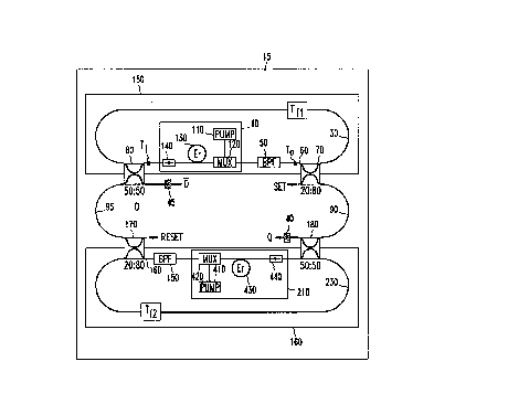
FIG. 2 shows a simplified schematic representation of an
illustrative arrangement of elements forming all-optical flip-flop 15,
including optical amplifiers 150 and 160, in accordance with the
principles of the invention. In optical amplifier 150, feedback path 30,
comprised of a doped or undoped optical fiber, couples the output of
erbium-doped fiber amplifier (EDFA) 10 to its input. It will be
appreciated by those skilled in the art that it may be desirable in some
applications, to use a rare-earth-doped fiber in feedback path 30 acting
as a saturable attenuator. The advantageous use of attenuators is
described in further detail below.
2135533
In the illustrative arrangement of FIG. 2, EDFA 10 is comprised of
pump 110, multiplexer 120, erbium-doped fiber 130, and optical isolator
140 arranged such that the light from pump 110 travels counter-
directionally with the signal. Each of these components and the
functions employed therein are well known in the art. In some
applications, it may be desirable to arrange the components in EDFA 10
in such a way that the light from pump 110 travels co-directionally, or
bi-directionally with the signal.
Optical bandpass filter 50 is positioned in forward path 60
between the output of EDFA 10 and output optical coupler 70. Forward
path 60 is comprised of an undoped optical fiber. Output optical coupler
70 couples a predetermined portion of the signal propagating in forward
path 60 to feedback path 30. Input optical coupler 80 couples a
predetermined portion of the signal propagating in feedback path 30 to
the input of EDFA 10. For purposes of this illustrative example, and not
as a limitation on the invention, output optical coupler 70 couples 20% of
the signal propagating in forward path 60 to feedback path 30 and 80%
of the signal to coupling fiber 90. Similarly, input optical coupler 80
couples 50% of the signal propagating in feedback path 30 to the input of
EDFA 10 and 50% of the signal to output port Q. In this example, both
output optical coupler 70 and input optical coupler 80 may be 7dB optical
couplers that are well known in the art.
In optical amplifier 160, feedback path 230, comprised of a doped
or undoped optical fiber, couples the output to the input of EDFA 210.
Feedback path 230 and EDFA 210 are identical to feedback path 30 and
EDFA 10, respectively, in optical amplifier 150 in structure and
operation. EDFA 210 is comprised of pump 410, multiplexer 420,
erbium-doped fiber 430, and optical isolator 440. These elements are
identical in structure and operation to those corresponding elements
comprising EDFA 10 as described above.
Optical bandpass filter 150 is positioned in forward path 160
between the output of EDFA 210 and output optical coupler 170. Optical
bandpass filter 150, forward path 160, and output coupler 170 are
identical to optical bandpass filter 50, forward path 60, and output
coupler 70, respectively, in optical amplifier 150 in structure and
operation. Output optical coupler 170 couples a predetermined portion of
the signal propagating in forward path 160 to feedback path 130. Input
21 3 55 3 3
optical coupler 180 couples a predetermined portion of the signal
propagating in feedback path 130 to the input of EDFA 210. Input
optical coupler 180 is identical to input optical coupler 80 in optical
amplifier 150 in structure and operation.
The output of optical amplifier 150 is coupled to the input of
optical amplifier 160 via output coupler 70, coupling fiber 90, and input
coupler 180. Similarly, the output of optical amplifier 160 is coupled to
the input of optical amplifier 150 via output coupler 170, coupling fiber
95, and input coupler 80. Coupling fibers 90 and 95 comprise undoped
optical fibers.
One end of coupling fiber 90 functions as the SET input port to
all-optical flip-flop and the other end of coupling fiber 90 functions as the
Q output port. One end of coupling fiber 95 functions as the RESET
input port to all-optical flip-flop 15 and the other end of coupling fiber 95
functions as the Q output port. Optical bandpass filter 40, tuned to pass
signal wavelengths substantially equal to lA, is positioned at the end of
coupling fiber 90 at the Q output port. Optical bandpass filter 45, tuned
to pass signal wavelengths substantially equal to 1B, is positioned at the
end of coupling fiber 95 at the Q output port.
In operation, when there is no optical pulse signal present at the
SET input, the amplified spontaneous emission (ASE) from EDFA 10 is
filtered at wavelength lA by optical bandpass filter 50 as it propagates
along forward path 60. ASE is generated by EDFA 10 from the
amplified light produced by the spontaneous emission of excited erbium
ions from erbium-doped fiber 130. As discussed above, 20% of the filtered
ASE is coupled from the output of EDFA 10 through output optical
coupler 70 to feedback loop 30. Input optical coupler 80 allows 50% of the
ASE to be re-injected as a feedback signal to the input of EDFA 10. This
feedback signal is sufficient to cause stimulated emission in EDFA 10
which results in self sustaining lasing output by optical amplifier 150 at
wavelength lA. The remaining 50% of the signal propagating in feedback
path 30 is coupled by input optical coupler 80 to the Q output port where
it is blocked by optical bandpass filter 45 since optical bandpass filter 45
is tuned to pass wavelengths at 1B and the signal has a wavelength of lA.
The following mathematical exposition should prove useful to one
skilled in the art in the understanding of the detailed operation of the
self sustaining laser operation discussed above. The input and output
21 355 3 3
6
photon fluxes to erbium-doped fiber 130 are related through coupled
implicit equations:
~a~; +g;
q~ut = q~ exp ~ (q~n - q'tut ) - a L i =1, 2, P ( 1)
a;
and
qin,out = ~ qin.out
a~
'
where ~,I is the wavelength of the input signal, ~,2 is the wavelength of
the output signal, ~,n is the wavelength of the pump light in EDFA 10, q
are the photon fluxes entering and exiting erbium-doped fiber 130, a and
g* are absorption and emission coefficients at the control and pump
wavelengths, respectively, z is a saturation parameter, and L is the
length of erbium-doped fiber 130.
Feedback path 30 fixes the relationship between input and output
of EDFA 10 at wavelength ~,z
rn =TT T.FF "wt=TFF "ut (3)
q~lz 'n out JI 'n nutq~z I 'n outq~z
where T,.n , and T"ut are the transmissivity of the optical components at the
input and output of EDFA 10, and TAI is the transmissivity of feedback
path 30, T, = T,nT,u'T~., and F,.n and F'~~, are the coupling ratios of input
optical coupler 80 and output optical coupler 70, respectively.
Equations ( 1) to (3) reduce to an explicit equation for the output
of EDFA 10 , valid above the lasing threshold, that depends linearly on
the pump and input signal powers:
out tut ~ 1 - F~ut ~ .n
Q>', = Qa_~I-H~ )+(1-F,n)T,nQ~n(1-H~, ) ~ , (a L-ln(TF F
1 - T FnFmt " ~ , a + ~'z I rn our
~z g~z
(4)
where the transfer function H~; is defined as:
a. +
Ha~ =a~l +g~, (a~~L-In(TF,nF'tuf)~-a~;L i=1, P (5)
A,
2135533
and Qa; are the photon fluxes entering and exiting EDFA 10. For
equations (4) and (5) to be valid, EDFA 10 must be operating as a laser
which requires that total gain through the combination of forward path
60 and feedback path 30 be equal or greater than unity. It will be
apparent to those skilled in the art that the gain through the
combination of forward path 60 and feedback path 30 may be readily
controlled by changing the fraction of light propagating in feedback path
30 by changing the coupling ratios of output coupler 70 and input
coupler 80. Alternatively, it may be desirable to include a controllable
attenuation element positioned in feedback path 30 to control the gain
through the combination of forward path 60 and feedback path 30.
FIG. 3 shows a graph of equation (4) where the calculated output
power of EDFA 10 in optical amplifier 150 is plotted as a function of
input signal power under the following illustrative conditions:
~, p = 980nm
~,, =1560nm
T~ =T~, =0.8
Tf = 0.5
F, =Fz =0.5
L=13m
~ = l.SxlO'Sm-'s-'
a = 0.38m-'
gi = 0.62m-'
IS
The slope (or "gain") of the transfer function Ha; is independent of
pump power and is determined by principally by the transmissivity
terms,T,n, T"u,, and T~,and coupling ratios F,~and F"u~. Indeed, where
y = ~.z, a~,~ = a~,z, and g~ = g~z , the gain transfer function reduces to:
dQ~~ _ ~I-Fn)(1-F~ur~ (6)
dQa~ T~ F,~F,N,
Thus, high transfer function gain is achieved with weak feedback
characterized by a small Tj.F,~F,~, term. This results because EDFA 10 is
clamped to high gain so that the input signal also experiences high gain
2135533
g
which readily saturates the output power of EDFA 10. It will be readily
appreciated to those skilled in the art that the TfF,.nF,,u, term may be
advantageously adjusted to alter the gain characteristics of all-optical
flip-flop 15 by changing, for example, transmissivity T~ of the feedback
path 30 by incorporating a controllable attenuation element into
feedback path 30. Alternatively, it may also be desirable to incorporate
other elements into feedback path 30 such as saturable or controllable
absorbers, and modulators.
Returning back to FIG. 2, output optical coupler 70 couples a
predetermined portion of the laser output of optical amplifier 150 to
coupling fiber 90. As stated above, for purposes of this example, output
optical coupler 70 couples 80% of the signal propagating in forward path
60 to coupling fiber 90. Input optical coupler 180 couples 50% of the
signal propagating in coupling fiber 90 to optical bandpass filter 40 as an
output at the Q output port. The remaining 50% of the signal is coupled
to the input of EDFA 210 in optical amplifier 160. This coupled laser
output from optical amplifier 150 saturates EDFA 210 so that the gain
through EDFA 210 is reduced below the threshold necessary for EDFA
210 to operate as a self sustaining laser in the manner described above.
Although EDFA 210 is saturated by the output of optical amplifier
150 to prevent lasing, the ASE generated in EDFA 210 propagates
through optical bandpass filter 150, where it is filtered at 1B. The ASE
then propagates along forward path 160 to output coupler 170. Output
coupler 170 couples 80% of this filtered signal to coupling fiber 95 and
optical bandpass filter 45 via input coupler 80 where it is output at the
Q output port. The remaining 20% of the signal from coupler 170 is
coupled to feedback path 230 and input coupler 180. Input coupler 180
couples 50% of the signal propagating in feedback path 230 to the Q
output port where it is blocked by optical bandpass filter 40 since optical
bandpass filter 40 is tuned to pass wavelengths at lA and the signal
propagating in feedback path 230 has a wavelength of 1B. The remaining
50% of the signal propagating in feedback path 230 is coupled by optical
coupler 180 as a feedback signal to the input of EDFA 210. This feedback
signal does not cause EDFA 210 in optical amplifier 160 to lase since
EDFA 210 is already saturated by the laser output of optical amplifier
150 as discussed above.
21 3553 3
9
Thus, in the first stable state of operation where optical amplifier
150 is lasing and optical amplifier 160 is saturated, all-optical flip-flop
15 generates a strong signal at the Q output port at wavelength lA, and a
weak signal at the Q output port at wavelength 1B. FIG. 4 is a graph of
the output power at the Q output port of all-optical flip-flop 15 when it is
operating in its first stable state of operation applying the illustrative
operating conditions described above when referring to FIG. 3, and
where lA=1544nm and 1B=1566nm. FIG. 4 shows the strong and narrow
peak that is characteristic of laser output.
FIG. 5 is a graph of the output power at the Q output port of all-
optical flip-flop 15 when it is operating in its first stable state of
operation. The power output here is sharply reduced as compared to the
Q output port because only ASE from EDFA 210 at wavelength 1B can
pass through optical bandpass filters 150 and 45. The extinction ratio
between Q and Q output ports has been shown to be typically about 40
dB under the illustrative operating conditions discussed when referring
to FIG. 3, and where lA=1544nm and 1B=1566nm. All-optical flip-flop 15
holds this first stable state of operation indefinitely, or until it is
switched to the second stable state of operation as discussed below.
All-optical flip-flop 15 is switched to its second stable state of
operation when an optical signal pulse, having a wavelength within the
gain bandwidth of EDFA 10, is received at the RESET port. Output
optical coupler 170 couples 80% of the optical signal pulse from the
RESET port to optical input coupler 80 via coupling fiber 95. Optical
input coupler 80 couples 50% of the pulse signal from coupling fiber 95
into the input of EFDA 10 in optical amplifier 150. If this pulse signal
coupled to the input of EFDA 10 is of sufficient power and duration, then
EDFA 10 becomes saturated which reduces the gain through EDFA 10
below the threshold necessary for optical amplifier 150 to operate as a
self sustaining laser in the manner described above. Under the
illustrative conditions described above when referring to FIG. 3 and
where lA=1544nm and 1B=1566nm, we have found that an optical signal
pulse with -8dBm input power with a minimum pulse duration of 100
msec is sufficient to saturate EDFA 10.
When EDFA 10 in optical amplifier 150 is saturated so that it
cannot lase, then its output to optical amplifier 160 via optical couplers
70 and 180 and coupling fiber 90 is no longer sufficient to saturate
l0 2135533
EFDA 210 in optical amplifier 160 below its lasing threshold. Optical
amplifier 160 is then free to lase in the ASE feedback manner described
above. Of course, optical amplifier 160 will lase at a wavelength 1B since
optical bandpass filter 150 is tuned to 1B.
The laser output of optical amplifier 160, at wavelength 1B, is
coupled to optical amplifier 150 via couplers 170 and 80 and coupling
fiber 95. This coupled laser output causes optical amplifier 150 to remain
saturated below is lasing threshold after the optical signal pulse at the
RESET port has elapsed.
Thus, in the second stable state of operation where optical
amplifier 160 is lasing and optical amplifier 150 is saturated, all-optical
flip-flop 15 generates a strong signal at the Q output port at wavelength
1B, and a weak signal at the Q output port at wavelength lA.
FIG. 6 is a graph of the output power at the Q output port of all
optical flip-flop 15 when it is operating in its second stable state of
operation applying the illustrative operating conditions described above
when referring to FIG. 3 and where lA=1544nm and 1B=1566nm. The
power output here is sharply reduced as compared to the Q output port
because only ASE from EDFA 10 at wavelength lA can pass through
optical bandpass filters 50 and 40.
FIG. 7 is a graph of the output power at the Q output port of all-
optical flip-flop 15 when it is operating in its second stable state of
operation. FIG. 6 shows the strong and narrow peak that is
characteristic of laser output. The extinction ratio between Q and Q
output ports has been shown to be typically about 40 dB under the
illustrative operating conditions discussed when referring to FIG. 3. All-
optical flip-flop 15 holds this second stable state of operation indefinitely,
or until it is switched to the first stable state of operation as discussed
below.
All-optical flip-flop 15 is switched to its first stable state of
operation when an optical signal pulse, having a wavelength within the
gain bandwidth of EDFA 210, is received at the SET port. Output optical
coupler 70 couples 80% of the optical signal pulse from the SET port to
optical input coupler 180 via coupling fiber 90. Optical input coupler
couples 50% of the pulse signal from coupling fiber 90 into the input of
EFDA 210 in optical amplifier 160. As before, when discussing the
switching from the first to second stable states, if this pulse signal
11 2135533
coupled to the input of EFDA 210 is of sufficient power and duration,
then EDFA 210 becomes saturated which reduces the gain through
EDFA 210 below the threshold necessary for optical amplifier 160 to
operate as a self sustaining laser. When optical amplifier 160 stops
lasing, then optical amplifier 150 is no longer saturated by the laser
output and becomes free to lase in the ASE feedback manner described
above. The laser output of optical amplifier 150, at wavelength lA, is
coupled to optical amplifier 160 via couplers 70 and 180 and coupling
fiber 90. This coupled laser output causes optical amplifier 150 to remain
saturated below is lasing threshold after the optical signal pulse at the
SET port has elapsed.
FIG. 8 is a graph of the transfer functions represented by equation
(5) for both optical amplifiers 150 and 160 showing the first and second
operating states for all-optical flip-flop 15 as points A and B. The
intersection of the transfer functions at point C represents an unstable
state of operation of all-optical flip-flop 15.
It will appreciated to those with skill in the art that all-optical
flip-flop 15 may be used to implement, in an all-optical manner, all of the
circuits presently implemented using electrical flip-flops. In addition,
when combined with the appropriate all-optical logic gates implemented
using all-optical inverters, as described in the co-pending U.S. patent
application Serial No. 168,291, all-optical flip-flip 15 can be used to
implement all-optical shift registers and bit-storage devices.
Those with skill in the art will also appreciate that all-optical flip
flop 15 may also be used to implement modulo-n (i.e., n-ary) optical logic
circuits by utilizing its mufti-wavelength operating characteristics. This
characteristic would enable modulo-n logic devices to be realized because
all-optical flip-flip 15 switches not only power at its outputs but also
wavelength.
The above-described arrangements are, of course, merely
illustrative of the application of the principles of the invention. Other
arrangements may be devised by those skilled in the art without
departing from the spirit or scope of the invention. For example, it will
be apparent to those skilled in the art that a semiconductor optical
amplifier may be advantageously employed in place of EDFA 10 and
EDFA 210 in FIG. 2 to allow substantially faster switching of all-optical
12 21 3 5 5 3 3
flip-flop 15. Such an all-optical flip-flop could thus be used in a photonic
integrated circuit chip.