Note: Descriptions are shown in the official language in which they were submitted.
~ 2l3s~g~
- WO 93/2~01~ PCT/U~93/04346
METHOD AND APPARATUS FOR SYNCHRONIZ~!JG
A SIMULCAST TRANSMISSION SYSTEM
Field of the Invention
This invention relates in general to simulcast transmissîon systems,
and more particularly to a method and apparatus for synchronizing
transmissions of a simulcast transmission system.
Background of the Invention
A number of methods have been proposed or are in use today for
- automatically synchronizing the message transmissions of transmitters
utilized in simulcast transmission systems. One such method includes a
15 master transmitter centrally located within a plurality of secondary
transmitters disposed in an annular fashion around the central
transmitter. The innermost arulular ring of transmitters was
synchronized to the master transmitter, while the remainder of the
system transmitters were disabled. The next adjacent annular band of
20 transmitters was then synchronized to the innerrnost annular band and
the process was repeated until every annular band in the system was
synchronized. Such a synchronizing arrangement guaranteed that
adja~ent annular bands were properly synchronized, however, such a
system cannot estimate the variations in delay which were introduced
25 because a common signal source for making the delay measurements
was not used.
Additionally~ current methods of synchronizing the plurality of
transmitters in a simulcast transmission system require a substantial
amount of time required to complete the propagation delay
3û measurement sequences. iFor a large simulcast transmission system,
such as one having forty transmitters, delay measurement times of forty
seconds and more were typical when each transmitter was sequentially
accessed for measuring the individual transmitter propagation delay.
- However, by splitting a simulcast system into the smaller transmission
35 regions, the delays could be simultaneously measured for regional
transmitters in alternate transmission regions thereby reducing the total
time required to synchronize transmissions within the system. This
213579~ ~' ~
Wo 93/25012 - PCI/US93/0434
method of measurement of the transmitter delaysJ although it speeded
up the delay measurement process, presented a new set of problems,
such as that of measuring the delays required to synchronize the
transmitters in adjacent transmission regions
Generally, to synchronize simulcast transmitters, the propagation
delay times must be measured for the plurality of transmitters in order to
account for propagation delay differences, however ,even when the
delays are measured, jitters received at each transmitter resulted in
indecisiveness in locating bit edges. That is, although the bit widths were
10 restored to their proper du~y cycle, the simulcast bit synchronization will
be less than the accuracy required because of ~mcertainty in locating the
bit edges at the transmitters.
To overcome the jitters at the plurality of base sites, synchronized
clocks were incorporated at the plurality of transmitters. The data to the
15 plurality of transmitters was sent faster than real time transmission on a
narrow band radio frequency (RF) channel and when the data was
received, it was stored in buffers at each of the plurality of transrnitters
until it was time for the simulcast transmission of the stored data. The
synchronized clocks at the plurality of transmitters are required to be
20 extremely accurate, and when all the synchronized clocks indicated a
predetermined time, the data was simultanec~usly transmitted by the
plurality of base sites. The problem of jitters was removed because the
data was locally genera~ed at the plurality of transmitters. However,
while there was no problem with jitters because the data is locally stored
25 and generated at the plurality of transmitters, a substantial amount of air
time was devoted to synchronize and resynchronize the plurality of
clocks located at each of the transmitters to ensure that the clocks are
accurately synchronized for the simulcast transmission of the data.
Thus, what is needed is a method and apparatus for synchronizing
30 and maintaining the synchronization of the plurality of transmitters in a
simulcast transmission system to avoid propagation delays and bit edge
jitters without sacrificing valuable air-time to obtain and maintain
synchronization.
.. . . -
f~`wo 93/25012 2 1 ~ ~ 7 9 ~ PCI /US93/04346
Summary of the Invention
A simulcast system has a transrx~itter controller capable of
measuring propagation delays to a plurality of base sites and calculating
propagation delay differences from the measured propagation delays for
each of a plurality of base sites. The transmi~ter controller also receives
and transmits data to each of the plurality of base sites. The plurality of
base sites have transmitters capable of transmitting data as radio
frequency transmission at substantially the same ~ime. The transmitter
controller comprises a transmitter which transmits the propagatis~n delay
differences, and a start command to the plurality of base sites for
initiating simulcast retransmission of the data. The plurality base sites
comprise receivers which receive the propagation delay differences, the
propagation delay differences being determined for delaying the
retransmission of data in each of the plurality of base sit~s. The base site
receivers receive data from the transmitter controller to be retransmitted
by the plurality of base sites. A memory at the base site stores the
received data and the base site receivers receive the start command. A
timer delays retransmission of the stored data from the receipt of the
2~ start coIrunand by the propagation delay difference calculated for each
base site to enable the retransrnission of the data at substantially the same
time by the plurality of base sites.
A method for synchronizing data transmissions in a simulcast
system, the simulcast system comprising a plurality of base sites coupled
to a transmitter controller capable of measuring propagation delays from
the transmitter controller to th~ plurality of base sites and calculating
propagation delay differences for each of the plurality of base sites, the
transmitter controller capable o receiving and transmitting data to eac}~
of the plurality of base sites, the plurality of base sites capable of
transmitting data as radio frequency transmission at substantially the
same time, the method comprising the steps of:
(a) transrnitting the propagation delay differences to the plurality
of base s*es;
(b) transmitting a start command to the plurality of base sites for
initiating simulcast transmission of the data;
WO 93/2s012 2 1 3 5 7 9 S PCr/US93/0434~
(c) receiving the transmitted data from the transmitter controller
- at each of the plurality of base sites;
(d) storing the received data at each of ~e plurality of base sites;
(e~ receiving the start command by the plurality of base sites for
5 ini~ating the simulcast retransmission of the stored data by the plurality
of base sites; and ~ ;
(f) delaying the retransmission of the store-d data by the plurality of
base sites from the receipt of the start command by the propagation delay
differences at the plurality of the base sites to enable retransmission of
the stored data at substantially the same time by the plurality of base sites.
Brief Description of the Drawings
FIG. 1 is an electrical block diagram of a data transmission system in
accordance wîth the preferred embodiment of the present invention.
FIG. 2 is an electrical block diagram of a terminal for processing and
transmitting message information in accordance with the preferred
embodiment of the present invention.
FIGS. 3-5 are timing diagrams illustrating the transmission format
of the signaling protocol utilized in accordance with the preferred
embodiment of the present invention.
FIGS. 6 and 7 are timing diagrams illustrating the synchronization
signals utilized in accordance with the preferred embodiment of the
present invention.
FIG. 8 is an electrical block diagram of a data communication
receiver in accordance with the preferred embodlment of the present
invention.
~IG. 9 is an electrical block diagram of a threshold level extraction
circuit utilized in the data communication receiver of FIG. 8.
FIG. 10 is an electrical block diagram of a 4-level decoder utilized in
the data communication receiver of FIG. 8.
FIG. 11 is an electrical block diagrarn of a symbol synchronizer '
utilized in the data communication receiver of FIG. 8. }
FIG. 12 is an electrical block diagram of a 4-level to binary converter ' `35 utilized in the data communication receiver of FIG. 8.
FIG. 13 is an electrical block diagram of a synchronization correlator
utilized in the data communication receiver of FIG. 8.
J
.
2135795 - .
` WO93/2~012 P~/US93/~4346
FIG. 14 is an electrical block diagram of a phase timing generator
utilized in the data communication receiver of FIG. 8.
FIG. 15 is a flow diagram illustrating the synchronization
correlation sequence in accordance with the preferred embodiment of the
5 present invention.
FIG. 16 is an electrical block diagram of a simulcast system for
processing and transmitting information in accordance with the
preferred embodiment of the present invention.
FIG. 17 is a flow diagram illustrating the synchronization sequence
10 for synchroniæing the plurality of base sites in accordance with the
preferred embodiment of the present invention.
Description of a Preferred Embodiment
FIG. 1 is an electrical block diagram of a data transmission system
100, such as a paging syster~, in accordance with the preferred
embodiment of the present invention. In such a data transmission
system 100, messages originating either from a phone, as in a system
providing numeric data transmission, or from a message entry device,
20 such as an alphanumeric data terminal, are routed through the public
switched telephone network (PSIN) to a pag~ng terminal 102 which
processes the numeric or alphanumeric message information for
transmission by one or more transmitters 104 provided within the
system. When multiple transmitters are utilized, the transmitters 104,
25 preferably in simulcast, transmit the message information to data
comrnunication receivers 106. Processing of the numeric and
alphanumeric informatic)n by the paging terminal 102 and the protocol
utilized for the transmission of the messages is described below.
~IG. 2 is an electrical block diagram of the paging terrninal 102
30 utilized for processing and controlling the transmission of the message
in~rmation in accordance with the preferred embodiment of the present
invention. Short messages, such as tone-only and numeric messages
which can be readily entered using a Touch-Tone telephone, are coupled
t-o the paging terminal 102 through a telephone interface 202 in a manner ,
35 well known in the art. Longer messages, such as alphanumeric messages
which require the use of a data entry device, are coupled to the paging
terminal 102 thrcugh a modem 206 using any of a number of well
2135795
WO 93/2~012 PCI/US93/~434~
known modem transmission protocols. When a call to place a message
is received, a controller 204 handles the processing of the message. The
controller 204 is preferably a microcomputer, such as an MC68000 or
equivalent, which is manufactured by Motorola Inc., and which runs
various pre-programmed routines for controlling such terminal
operations as voice prompts to direct the~aller to enter the message, or
the handshaking protocol to enable reception of messa~es from a data
entry device. When a call is received, the controller 204 references
information stored in the subscriber database 208 to determine how the
message being received is to be processed. The subscriber database 208
includes, but is not limited to, such information as addresses assigned to
the data communication receiver, message type associated with the
address, and information related to the status of the data communication
receiver, such as active or inactive for failure to pay the service charges.
A data entry terminal 240 is provided which couples to the controller
204, and which is used for such purposes as entry, updating and deleting
of information stored in the subscriber data base 208, for monitoring
system performance, and for obtaining such information as ser~rice
charge information.
The subscriber database 208 also indudes such information as to
what transmission frarne and to what trans~ission phase the data
communication receiver is assigned, as will be described in further detail
below. The received message is stored in an active page file 210 which
stores the messages in queues according to the transmission phase
assigned to the data communica~on receiver. In the preferred
embodiment of the present invention, four phase queues are provided
in the active page file 210. The active page file 210 is preferably a dual
port, first in first out random access memory, although it will be
appreciated that other Tandom access memory devices, such as hard disk
drives, can be utilized as well. Periodically, the message information
stored in each of the phase queues is recovered from the active page file
210 under control of controller 204 using timing information such as
provided by a real time dock 214, or other suitable timing source. The
recovered message information from each phase queue is sorted by
frame number and is then organized by address, message information,
and any other information required for transmission, and then batched
into frames based upon message size by frame batching controller 212.
213~79S
WO 93~25012 PCr/US93/û4346
The batched frame information for each phase queue is coupled to frame
message buffers 216 which temporarily store the batched frame
information until a time for further processing and transmission.
Frames are batched in numeric sequence, so that while a curren~ frame is
being transmitted, the next frarne to bè transmitted is in the frame
message buffer 21~, and the next frame thereafter is being retrieved and
batched. At the appropriate time, the batched frame information stored
in the frame message buffer 216 is transferred to the frame encoder 218,
again maintaining the phase queue relationship. The frame encoder 218
encodes the address and message information into address and message
code words required for transmission, as will be desaibed below. The
encoded address and message code words are ordered into blocks and
then coupled to a block interleaver 220 which interleaves preferably eight
code words at a time for transmission in a manner well known in the
art. The interleaved code words from each block interleaver 220 are then
serially transferred to a phase multiplexer 221, which multiplexes the
message information on a bit by bit basis into a serial data stream by
transmission phase. The controller 204 next enables a frame sync
generator ?'7~ which generates the synchror~ization code which is
transmitted at the start of each frame transmission. The synchronization
code is multiplexed with address and messa~e information under the
control of controller Z04 by serial data splicer 224, and generates
therefrom a message stream which is properly formatted for
transmission. The message stream is next coupled to a transmitter
controller 226, which under the control of controller 204 transmits the
message stream over a distribution channel 228. The distribution
channel 228 may be any of a number of well known distribution channel
types, such as wire line, an RF or microwave distribution channel, or a
satellite distribution~link. The distributed message stream is transferred
to one or more transmitter stations 104, depending upon the size of the
communication system. The message stream is first transferred into a
dual port buffer 230 which temporarily stores the message stream prior to
transmission. At an appropriate time determined by timing and control
circuit 232, the message stream is recovered from the dual port buffer 230
and coupled to the input of preferably a 4-level FSK modulator 234. The
modulated message stream is then coupled to the transmitter 236 for
transmission via antenna 238.
213~7`95
WO 93/25012 PCI/US93/0434
FIGS. 3, 4 and 5 are timing diagrams illustrating the transmission
format of the signaling protocol utilized in accordance with the preferred
embodiment of the present invention. As shown in FIG. 3, the signaling
protocol enables message transmission to dat~: communication receivers,
5 such as pagers, assigned to one or more of 128 frames which are labeled
frame 0 through frame 127. It then will b~ appreciated that the actual
number of frames provided within the ~i`gnaling protocol can be greater
or less than described above. The greater the number of frames utilized,
the greater the battery life that may be provided to the data
10 communication receivers operating within the system. The fewer the
number of frames utilized, the more often messages can be queued and
deliYered to the data communication receivers assigned to any particular
frame, thereby reducing the latency, or time required to deliver messages.
As shown in FIG. 4, the frames comprise a synchronization code
15 (sync) followed preferably~by eleven blocks of message informati 3n
which are labeled block 0 through block 1~. As shown in FIG. 5, each
block of message information comprises preferably eight address, control
or data code words which are labeled word 0 through word 7 for each
phase. Consequently, each phase in a frame aIlows the tTansmission of
20 up to eighty-eight address, control and data code words. The address,
control and data code words are preferably 3~,21 BCH code words with an
added thirty-second even parity bit which provides an extra bit of
distance to the code word set. It will be appreciated that other code
words, such as a 23,12 Golay code word, could be utilized as well. Unlike
25 the well known POCSAG signaling protocol which provides address and
data code words that utilize the first code word bit to define the code
word type as either address or data, no such distinction is provided for
the address and data code words in the signaling protocol utilized with
the preferred embodiment of the; present invention. Rather, address and
30 data code words are defined by their position within the mdividual
frames.
FIGS. 6 and 7 are timing diagrams illustrating the synchronization
code utilized in accordance with the preferred embodiment of the
present invention. In particular, as shown in FIG. 6, the synchronization
35 code comprises preferably three parts, a first synchronization code (sync
1), a frame information code word (frame info) and a second
synchronization code (sync 2). As shown in FIG. 7, the first
2135795 il ~
WO 93/25012 PCT~US93/04346
synchronization code comprises first and third portions, labeled bit sync 1
and BSl, which are alternating 1,0 bit patterns which provides bit
synchronization, and second and fourth portions, labeled "A" and its
complement "A bar", which provide frame synchronization. The second
5 and fourth portions are preferably single 32,21 BCH code words which are
predefined to provide high code word correlation reliability and which
are also used to indicate the data bit rate at which addresses and messages
are transmitted. The table below defines the data bit rates which are used
in conjunction with the signaling protocol.
Bit Rate "A" Value
1600bps Al and Al bar
3200 bps A2 and A2 bar
6400 bps A3 and A3 bar
Not defined A4 and A4 bar
As shown in the table above, three data bit rates are predefined for
address and message transmission, although it will be appreciated that
more or less data bit rates can be predefined as well, depending upon the
system requirements. A fourth "A" value is also predefined for future
use.
The frame information code word is preferably a single 32,21 BCH
code word which includes within the data portion a predeterrnined
number of bits reserved to identify the frame number, such as 7 bits
encoded to define frame number 0 to frame number 127.
The structure of the second synchronization code is preferably
similar to that of the first synchronization code described above.
However, unlike the first synchronization code which is preferably
transmitted at a fixed data!symbollrate~ such as 1600 bps Cbits per second~,
the second synchronization code is transmitted at the data syrnbol rate at
- which the address and messages are to be transmitted in any given
frame. Consequently, the second synchronization code allows the data
communication receiver to obtain "fine" bit and frame synchronization
at the frame transmission data bit rate.
In summary, the signaling protocol utilized with the preferred
embodiment of the present invention comprises 128 frames which
include a predetermined synchronization code followed by eleven data
213579~ ~
WO 93/25012 PCr/US~3/04346~'
blocks which comprise eight address, control or message code words per
phase. The synchronization code enables identification of the data
transmission rate, and insures synchronization by the data
communication receiver with the data code words transmitted at the
5 various transmission rates. i~
FIG. 8 is an electrical block diagram of the data communication
receiver 106 in accordance with the preferr~~embodiment of the present
invention. The heart of the data communication receiver 106 is a
controller 816, which is preferably implemented using an
MC68HC05HC11 microcomputer, such as manufactured by Motorola, Inc.
The microcomputer controller, hereinafter call the controller 816,
receives and processes inputs from a number of peripheral circuits, as
shown in FIG. 8, and controls the operation and interaction of the
peripheral circuits are achieved by using software subroutines. The use
of a microcomputer controller for processing and control functions is
well known to one of ordinary skill in the art.
The data communication receiver 106 is capable of receiving
address, control and message information, hereafter called "data" which
is modulated using preferably 2-level and ~level frequency modulation
techniques. The transmitted data is intercepted by an antenna 802 which
couples to the input of a receiver section 804. Receiver section 804
processes the received data in a manner well known in the art, providing
at the output an analog 4-level recovered data signal, hereafter called a
recovered data signal. The recovered data signal is coupled to one input
of a threshold level extraction circuit 808, and to an input of a 4-level
decoder 810. The threshold level extraction circuit 808 is best understood
by referring to ~IG. 9, and as shown, comprises two clocked level detector
circuits 902, 904 which have as inputs the récovered data signal. Level
detector 902 detects the peak signal arnplitude value and provides a high
peak threshold signal which is proportional to the detected peak signal
amplitude value, while level detector 904 detects the valley signal
amplitude value and provides a valley threshold signal which is
proportional to the detected valley signal amplitude value of the
recovered data signal. The level detector 902, 904 signal outputs are
coupled to terminals of resistors 906, 912, respectively. The opposite
resistor terminals 906, 912 provide the high threshold output signal (Hi),
and the low threshold output signal (Lo), respectively. The opposite
213~795
WO 93/25012 PcrtUS93/o43~6
11 !
resistor terminals 906, 912 are also coupled to terminals of resistors 908,
910, respectively. The opposite resistor 90B, 910 terminals are coupled
together to form a resistive divider which provides an average threshold
output signal (Avg) which is propor~onal to the average value of the
recovered data signal. Resistors 906, 912 have resistor values preferably
of lR, while resistors 908, 910 have resistoF values preferably of 2R,
realizing threshold output signal values of 17%, 50% and 83%, and
which are utilized to enable decoding the ~level data signals as will be
described ~elow.
When power is initially applied to the receiver portion, as when the
data communication receiver is first turned on, a clock rate selector 914 is
preset through a control input (center sample) to select a 128X clock, i.e. a
clock having a frequency equivalent to 128 times the slowest data bit rate,
which as described above is 1600 bps. The 128X clock is generated by 128X
clock gea~erator 844, as shown in FIG. 8, which is preferably a crystal
controlled oscillator operati~g at 204.8 ~CHz (kilohertz). The output of
the 128X clock generator 844 couples to an input of frequency divider 846
which divides the output frequency by two to generate a 64X clock at
102.4 KHz. Returning to FIG. 9, the 128X clock allows the level detectors
902, 904 to asynchronously detect in a very short period of time the peak
and valley signal amplitude values, and to th~refore generate the low
(Lo), average (Avg) and high (Hi) threshold output signal values
required for modulation decoding. ~fter symbol synchronization is
achieved with the synchronization signal, as will be described below, the
controller 816 generates a second control signal (Center Sample) to enable
selection of a 1>C symbol clock which is generated by symbol synchronizer
812 as shown in FIG. 8.
Returning to FIG. 8, the 4-level decoder 810 operation is best
understood by referring to FIG. 10. As shown, the 4-level-decoder 810
comprises three voltage comparators 1010, 1020, 1030 and a symbol
decoder 1040. The recovered data signal couples to an input of the three
comparators 1010, 1020, 1030. The high threshold output signal (Hi)
couples to the second input of comparator 1010, the average threshold `.
output signal (Avg) couples to the second input of comparator 1020, and L
the low threshold output signal (Lo) couples to the second input of
comparator 1030. The outputs of the three comparators 1010, 1020,1030
213S79S ~ --
WO 93/2~012 PCr/US~/04346
12
couple to inputs of symbol decoder 1040. The symbol decoder 1040
decodes the inputs according to the table provided below.
Threshold Output
Hi Avg Lo MS13 LSB
RCin ~ R~in ~ RCin ~ ' O O
RCin < RCin ~ RCin ;,
Rcin ~ Rcin > RCin >
RCin > RCin > RCin > 1 0
As shown in the table above, when the recovered data signal
(RCiI,) is less than all three threshold values, the symbol generated is 00
(MSB = 0, LSB = 0). Thereafter, as each of the three threshold vallles is
exceeded, a different symbol is generated, as shown in the table abo~7e.
The MSB output from the 4-level decoder 810 is coupled to an input
of the symbol synchronizer ~12 and provides a recovered data input
generated by detecting the zero crossings in the 4-level recovered data
signal. The positive level of the recovered data input represents the two
positive deviation excursions of the analog ~level recovered data signal
above the average threshold output signal, and the negative level
represents the two negative deviation excursi~ns of the analog 4-level
recovered data signal below the average threshold output signal.
The operation of the symbol synchronizer 812 is best understood by
referring to FIG. l1. The 64X clock at 102.4 KHz which is generated by
frequency divider 846, is coupled to an input of a 32X rate selector 1120.
The 32X rate selector 1120 is preferably a divider which provides selective
division by 1 or 2 to generate a sample clock which is thirty-two times the
symbol transmission rate. A control signal (1600/3200) is coupled to a
second input of the 32X~rate selector 1120, and is used to select the sample
clock rate for symbol transmission rates of 1600 and 3200 symbols per
second. The selected sample clock is coupled to an input of 32X data
oversampler 1110 which samples the recovered data signal (MSB) at
thirty-two samples per symbol. The syrnbol samples are coupled to an
input of a data edge detector 1130 which generates an output pulse when
a symbol edge is detected. The sample clock is also coupled to an input of
a divide-by-16/32 circuit 1140 which is utilized to generate lX and 2X
symbol clocks synchronized to the~recovered data signal. The divide-by-
~o 93/2s0~2 2 1 3 5 7 9 ~ Pcr/Us93/04346 ~
13
16/32 circuit 1140 is preferably an up/down counter. When the data edge
detector 1130 detects a symbol edge, a pulse is generated which is gated by
AND gate 1150 with the curren~ count of divide-by-16/32 circuit 1140.
Concurrently, a pulse is generated by the data edge detector 1130 which is
also coupled ~o an input of the divid~by-16/32 circuit 1140. When the
pulse coupled to the input of AND gate 1150 arrives before the
generation of a count of thirty-two by the divide-by-16/32 circuit 1140, the
output generated by AND gate 1150 causes the count of divide-by-16/32
circuit 1140 to be advanced by one count in response to the pulse which is
coupled to the input of divid~by-16/32 circuit 1140 from the data edge
detector 1130, and when the pulse coupled to the input of AND gate 1150
arrives after the generation of a count of thirty-two by the divide-by-
16/32 circuit 1140, the output generated by AND gate 1150 causes the
count of divid~by-16/32 circuit 1140 to be retarded by one count in
response to the pulse which.is coupled tv the input of divide-by-16/32
circuit 1140 fro~ the data eclge detector 1130, thereby enabling the
synchronization of the 1X and 2~C symbol clocks with the recovered data
signal. The symbol clock rates generated are best understood from the
table below.
Input Control Rate Rate " 2X lX
Clock Input SelectorSelector Symbol Symbol
Divide Output Clock Clock
(Reiative) (SPS) Ratio (BPS) (BPS)
-- _ _ _ _ _ _~ _ ~ _ _ _
64X 1600 by 2 32X 3200 1600
64X 3200 by 1 64X 6400 3200
As shown in the table above, the lX and Z~ symbol clocks are
gener~ted at 1600, 3200 and 6400 bits per second and are synchronized
with the recovered data signal.
The 4-level binary converter 814 is best understood by referring to
FIG. 12. The lX symbol clock is coupled to a first clock input of a dock
rate selector 1210. A 2X symbol clock also couples to a second clock input
of the clock rate selector 1210. The symbol output signals (MSB, LSB) are
coupled to inputs of an input data selector 1230. A selector signal (2L/4L)
is coupled to a selector input of the clock rate selector 1210 and the
WO 93/2~012 2 1 3 5 7 9 ~ Pcr/us93/û4346~
14
selector input of the input data selector 1230, and provides control of the
conversion of the symbol output signals as ei~er 2-level FSK data, or 4-
level FSK data. When the 2-level FSK data conversion (2L) is selected,
only the MSB output is selected which is coupled to ~e input of a
5 parallel to serial converter 1~20. The 1X clock Lnput is selected by clock
rate selector 1210 which results in a single bit binary data s~eam to be
generated at the output of the parallel to serial converter 1220. When the
4-level FSK data conversion (4L) is selected, both the LSB and MSB
outputs are selected which are coupled to the inputs of the parallel to
serial converter 1220. The 2X clock input is selected by clock rate selector
1210 which results in a serial two bit binary data stream to be generated at
2X the symbol rate, which is provided at the output of the parallel to
serial converter 1220.
Returning to FIG. 8, the serial binary data stream generated by the 4-
level to binary converter 814 is coupled to inputs of a synchronization
word correlator 818 and a demultiplexer 820. The synchronization word
correlator is best understood with reference to FIG. 13. Predetermined
"A" word synchronization patterns are recovered by the controller 816
from a code memory 822 and are coupled to an "A" word correlator 1310.
- 20 When the synchronization pattern received matches one of the
predetermined "A" word synchronization paRerns within an acceptable
margin of error, an "A" or "A bar" output is generated and is coupled to
controller 816. The particular "A" or "A-bar" word synchronization
pattern correlated provides frame synchroniza~on to the start of the
frame ID word, and also defines the data bit rate of the message to follow,
as was previously described.
The serial binary data stream is also coupled to an input of the
frame word decoder 13~0 which decodes the frame word and provides an
indication of .the frame number currently being received by the
controller 816. During sync acquisitîon, such as following initial receiver
turn-on, power is supplied to the receiver portion by battery saver circuit
848, shown in FlG. 8, which enabled the reception of the "A"
synchronization word, as described above, and which continues to be
supplied to enable processing of the remainder of the synchronization
code. The controller 816 compares the frame number currently being
received with a list of assigned frame numbers stored in code memory
822. Should the currently received frame number differ from an
213~79~ 1
~YO 93/250~2 P~/US93/04346
assigned frame number, the cont~oller 816 generates a battery saving
signal which is coupled to an input of battery saver circuit 848,
suspending the supply of power to the receiver portion. The supply of
power will be suspénded until the next frame assigned to the receiver, at
5 which time a battery saver signal is generated by the controller 816 which
is coupled to the battery- saving circuit 848 to enable the supply of power
to the receiver portion to enable reception of the assigned frame.
Returning to the operation of the synchronization correlator shown
in ~IG. 13, a predetermined "C" word synchronization pattern is
reco~7ered by the controller 816 from a code memory 822 and is coupled
to a "C" word correlator 1330. When the synchronization pattern
received matches the predetermined "C" word synchronization pattern
with an acceptable margin of error, a "C" or "C-bar" output is generated
which is coupled to controller 816. The particular "C" or "C-bar"
synchronization word correlated provides "fine" frame synchronization
to the start of the data portion of the frarne.
Returning to FIG. 8, the start of the achlal data portion is established
by the controller 816 generating a block start signal (Blk Start) which is
coupled to inputs of a word de-interleaver 824 and a data recovery timing
circuit 826. The data recovery timing circuit 826 is best understood by
referring to FIG. 14. A control signal (2L / 4Lris coupled to an input of
clock rate selector 1410 which selects either lX or 2~ symbol clock inputs.
The selected symbol clock is coupled to the input of a phase generator
1430 which is preferably a docked ring counter which is clocked to
generate four phase output signals (01-04). A block start signal (BLK
START) is also coupled to an input of ~e phase generator 1430, and is
used to hold the ring counter in a predetermined phase until the actual
decoding of the message information is to begin. When the block start
signal releases the phase generator 1430, the phase generator 1430 begins
generating clocked phase signals which are synchronized with the
incomin~ message symbols.
Referring back to FIG. 8, the clocked phase signal outputs are
coupled to inputs of a phase selector 828. During operation, the
controller 816 recovers from the code memory 822, the transmission
phase number to which the data communication receiver is assigned.
The phase number is transferred to the phase select output (0 Select) of
the controller 816 and is coupled to an input of phase selector 828. A
wO 93/250l2 2 1 3 5 7 9 5 16 PCrlUS931W346~f
phase clock, corresponding to the transmission phase assigned, is
provided at the output of the phase selector 828 and is coupled to clock
inputs of the demultiplexer 820, block de-;nterleaver 824, and address
and data decoders 830 and 832, respectively. The demultiplexer 820 is
5 used to select the binary bits associated with the assigned transmission
phase which are then coupled to the input of block d~interleaver 824,
and clocked into the de-interleaver array on each corresponding phase
clock. The d~interleaver array is an 8x3~ bit array which d~interleaves
eight interleaved address, control or message code words, corresponding
10 to one transmission block~ The d~interleaved address code words are
coupled to the input of address correlator 830. The controller 816
recovers the address patterns assigned to the data communication
receiver, and couples the patterns to a second input of the address
correlator. When any of the de-interleaved address code words matches
15 any of the address patterns assigned to the data communication receiver
within an acceptable margin of error, the message information associated
with the address is then decoded by the data decoder 832 and stored in a
message memory 850 in a manner well known to one of ordinary skill in
the art. Following the storage of the message information, a sensible
20 alert signal is generated by the controller 816. The sensible alert signal ispreferably an audible alert signal, although i~will be appreciated that
other sensible alert signals, such as tactile alert signals, and visual alert
signals can be generated as well. The audible alert signal is coupled by
the controller 816 to an alert driver 834 which is used to drive an audible
25 alerting device, such as a speaker or a transducer 836. The user can
override the alert signal generation through the use of user input
controls 838 in a manner well known in the art.
Following the detection of an address associated with the data
communication receiver, the message information is coupled to the
30 input of data decoder 832 which decodes the encoded message
information into preferably a BCD or ASCII format suitable for storage
and subsequent display. The stored message information can be recalled
by the user using the user input controls 838 whereupon the controller
816 recovers the message information from memory, and provides the
35 message information to a display driver 840 for presentation on a display
842, such as an LCD display.
21~579S
~ ~ WO 93~25012 Pcr/u~g3/~4346
17
FIG. 15 is a flow chart describing the operation of the data
communication receiver in accordance with the preferred embodiment
of the present invention. At step 1502, when the data communication
receiver is turned on, the controller operation is initialized, at step 1504.
5 Power is periodically applied to the receiver portion to enable receiving
information present on the assigned R~ channel. When data is not
detected on the channel in a predetermined time period, battery saver
operation is resumed, at step 1508. When data is detected on the
channel, at step 1506, the synchronization word corre}ator begins
10 searching for bit synchronization at step 1510. When bit synchronization
is obtained, at step 1510, the "A" word correlation begins at step 1512.
When the non-complemented "A" word is detected, at step 1514, the
message ~ansmission rate is identified as described above, at step 1516,
and because frame synchronization is obtained, the time (T1) to the start
15 of the frame identification code word is identified, at step 1518. When
the non-complemented "A"~word is not detected, at ~tep 1514, indicating
the non-complemented "A" word may have been corrupted by a burst
error during transmission, a determination is made whether the
complemented "A" bar" is detected, at step 1520. When the "A bar" word
20 is not detected at step 1512, indicating that the "A-bar" word may also
have been corrupted by a burst error during kansmission, battery saver
operation is again resumed, at step 1508. When the "A-bar" word is
detected, at step 1520, the message transmission rate is identified as
described above, at step 1522, and because frame synchronization is
obtained, the time (T2) to the start of the frarne identification code word
is identified, at step 1524. At the appropriate time, decoding of the frame
identification word occurs, at step 1526. When the frame ID detected is
not one assigned to the data communication receiver, at step 1528, battery
saving is resumed, at step 1508,~arld remainsso until the next assigned
30 frame is to be received. When the decoded frame ID corresponds to an
assigned frame ID, at step 1528, the message reception rate is set, at step
1530. An attempt to bit synchronize at the message transmission rate is
next made at step 1532. When bit synchronization is obtained, at step
1533, the "C" word correlation begins at step 1534. When the non-
35 complemented "C" word is detected, at step 1536, frame synchronizationis obtained, and the time (T3) to the start of the message information is
identified, at step 1538. ~~"
WO 93/25012 2 1 3 ~ 7 9 ~ PCr/US93/04346~
18
When the non-complemented "C" word is not detected, at step 1536, ; ~indicating the non-complemented "C" word may have been corrupted by -
a burst error during transmission, a determination is made whether the
complement "C bar" is detected, at step 1540. When the "C bar" word is
5 not detected at step 1540, indicating that the "C-bar" word may also have
been corrupted by a burst error during.transmission, battery saver
operation is again resumed, at step 1508. When the "C-bar" word is
detected, at step 1540, frame synchronization is obtained, and the time
(T4) to the start of the message infonnation is identified, at step 1542. At
10 the appropriate time, message decoding can begin at step 1544.
In summary, by providing multiple synchronization code words
which are spaced in time, the reliability of synchronizing with
synchronization information that is subject to burst error corruption is
greatly enhanced. The use of a predetermined synchronization code word
15 as the first synchronization code word, and a second predetermined
synchronization code wordi which is the complement of the first
predetermined synchronization code word, allow accurate frame
synchronization on either the first or the second predetermined
synchronization code word. By encoding the synchronization code words,
20 additional information, such as ~e transmission data rate, can be
provided, thereby enabling the transmission~f message information at ;
several data bit rates. By using a second coded synchronization word pair,
"fine" frame synchronization at the actual message transmission rate can
be achieved, and as above, due to spacing in time of the synchronization
code words, the reliability of synchronizing at a different data bit rate with
synchronization information which is subject to burst error corruption is
greatly enhanced, thereby improving the reliability of the data
conununication receiver to receive and present messages to the receiver
user. , ~ ~
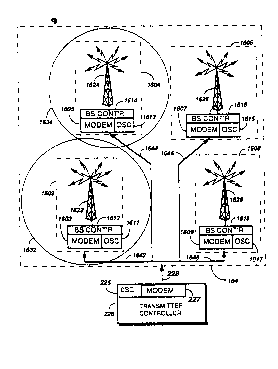
FIG. 16 is an electrical block diagram of a simulcast system for
processing and transmitting information in accordance with the
preferred embodiment of the present invention. In the simulcast
system, the transmitter stations 104, shown in PIG. 2, are coupled to a
transmitter controller 226. The transmitter controller 226 preferably
comprises a high speed modem 227 for transmitting data at a speed faster
than the speed of real-time transmission on a narrow band RF channel.
It will be appreciated by one of ordinary skill in the art that the high
~ 213~79~ .
`~ WO 93/2~012 ~ PCI/US93/04346
19
speed modem 227 time compresses the data before transmission to the
plurality of base sites 1602, 1604, 1606, 1608 to achieve this high speed
transmission. The transmitter controller 2~6 also includes an oscillator
225 for establishing a time stability or time reference of the transmitter
controller 226. A stability factor usually referred to as N parts-per-
million (PPM) or N parts-per-billion (PPB), where N refers to the
accuracy of the oscillator as the number of clock cycles. The transmitter
controller 2~6 is coupled by the distribution channel 228 to the plurality
of base sites 1602,1604,1606,1608 which are shown only as example. The
distribution channel 228 is shown divided into four distributor channels
1642-8 coupled to each of the base sites 1602, 1604, 1606, 1608, respectively.
The plurality of base sites 1602, 1604, 1606, 1608 comprise base site
controllers 1612, 1614, 1616, 1618 coupled to transmitters 1622-28 which
have predefined coverage areas, for example, coverage areas 1632, 1634.
The base site controllers 1612, 1614, 1616, 1618 also comprise modems
1603, 1605, 1607, 1609 for rèceiving the high speed data, and oscillators
1611, 1613, 1615, 1617 for establishing a time stability in the plurality of
base sites 1602, 1604, 1606, 1608. The base site controllers 1612, 1614, 1616,
1618 are preferably digital signal processors or microcomputers, such as
an MC68000 or equivalent, which are manufactured by Motorola Inc.,
and which run various pre-programmed ro~tines for controlling such
base station operations for transmitting and receiving data, or the
handshaking protocol to enable the retransmission of the data at a
predetermined time as will be discussed below.
FIG. 17 is a flow diagram illustrating the synchronization sequence
for synchronizing the plurality of base sites in accordance with the
preferred embodiment of the present invention. Operationally, the
transmitter controller measures each of the propagation delays for
transrnitting data to each of the plurality of base sites, step 1702.
Subsequent to measuring the propagation delays for transmitting data to
each of the plurality of base sites, the transmitter controller calculates
(computes) any propagation delay differences for each of the plurality of
base sites, step 1704. For example, the transmitter controller determines
the maximum measured propagation delay and subtracts all other
measured propagation delays to established the propagation delay
differences of each base site. This simple method would then include a
propagation delay difference of zero for the base site having the
wo 93l250l2 2 1 3 ~ 7 9 5 PCr~Uss3/04346~
maximum measured propagation delay. Each of the calculated
prop gation delay differences is transmitted to the corresponding base
site, step 1706. The transmitter controller is capable of sorting the
plurality of propagation delay differences to ensure that each base site
5 receives the propagation delay difference calculated between the
transmitter controller and that base site. The base sites receive and store
the propagation delay differences at eac~i of the respective base sites, step
1708. In step 1710, the transmitter controller receives data to be
transmitted to the plurality of base sites and transmits the received data
10 to the plurality of base sites, step 1712. The data is preferably transmittedby high speed rnodems at speeds faster than the speed of RF transmission
on a narrow band RF channel, a technique well known to one of
ordinary skill in the art. The data is time-compressed by well known
techniques before it is transmitted to the plurality of base sites. The
15 plurality of base sites receive the data, step 1714, and store the received
data in memory at each of the plurality of base sites, step 1716. Each of
the plurality of base sites has the capability of decompressing the time
compressed data received from the transmitter controller. Subsequent to
transmitting the data, the transmitter controller generates a start
20 command which is transmitted in simulcast to the plurality of base sites,
step 1718. The transmitter controller, before~transmitting the start
command, delays or waits a period of time to ensure that the plurality of
base sites receive, decompress and store the data. When the plurality of
base sites receive the start command, step 1720, each of the plurality of
25 base sites delays retransmission of the stored data by the propagation
delay difference calculated and stored in each base site, step 1722. The
propagation delay differences are calculated such that when all the base
sites receive the start command, all of the propagation delay differences
will expire simultaneously to ~nable simulcast retransmission of the
30 stored data from the plurality of base sites. When the difference
propagation delays expire at each of the plurality of base sites, each base
site retransmits the data stored in memory, step 1724. The data is
retransmitted via RF transmission by the plurality of base sites.
In summary, the simulcast system calculates propagation delay
35 differences from measured propagation delays for each of a plurality of
base sites. A terminal controller receives and transmits data to each of
the plurality of base sites. The terminal controller transmits the
f,.~ 2135795
~-- WO 93/2~012 PCr/US93/04346 :~
21
propagation delay differences and a start command to the plurality of
base sites for initiating simulcast retransmission of the data. The
plurality of base sites receive the propagation delay differences, the
propagation delay differences being determined for delaying the
5 retransmission of data in each of the plurality of base sites. The base site
stores the received data and delays retransmission of the stored data from
the receipt of the start command by ~e propagation delay difference
calculated for each base site to enable the retransmission of the data at
substantially the same time by the plurality of base sites.
Therefore, since the data is received and stored at the plurality of
base sites, jitters (i.e., bit edge uncertainty) is eliminated. This method
avoids resolving the difference in time the data is received at the
plurality of base sites by storing the received data and waiting a sufficient
length of time ~ ensure that all base sites have received the data to be
15 retransmitted. The data is also transmitted to the plurality of base sites
without regard to simulcast~reception or transmission of data. Also,
because the data is transmitted faster than the speed capable using an RF
transmission on a narrow band RF channei, by the time the data is
sirnulcast, the base site can start receiving additional data to be
20 retransmitted. In this way, the simulcast transmission system spends far
less time to synchronize the plurality of base~sites, thus saving valuable
air-time for transmitting and retransmitting the data instead of
synchronizing the system.
What is claimed is: