Note: Descriptions are shown in the official language in which they were submitted.
2136580
~ 1 -
Gallium Oxide Coatings for Optoelectronic Devices
Technical Field
This invention concerns electronic and optoelectronic devices provided
with a gallium oxide coating for improved performance.
5 Background of the Invention
Dielectric coatings play an important role in achieving desired
performance of III-V or II-VI semiconductor optoelectronic devices. Dense, closely
packed thin films are required to protect the surface, such as light emitting orreceiving facets, of optoelectronic devices from cont~min~tion and oxidation.
10 Antireflection coatings (AR) are required on light emitting or receiving facets to
increase the quantum efficiency of optoelectronic devices. Dielectric thin filmsproviding low midgap interface state density are required, in particular on light
emitting facets, to minimi7e nonradiative energy-dissipating processes such as
carrier recombination via interface states. Carrier recombination is known to trigger
15 a process at laser facets called thermal runaway causing device failure especially
when operated at high optical power. Inversion channel field effect devices require
dielectric films providing an unpinned Fermi level and low density of interface states
below midgap (p-channel device) or above midgap (n-channel device) at the
dielectric/semiconductor interface. Further, hysteresis-free capacitance-voltage20 characteristics with excellent reproducibility of flatband voltage, small flatband
voltage shift, and small frequency dispersion are required. Also, passivation ofstates on exposed surfaces of electronic III-V devices require low density of midgap
interface states.
A variety of materials has been proposed for such layers including
25 ZrO 2, Al 2 O 3, SiO x, SiN x, SiN x ~ y, Y 2 O 3 stabilized ZrO 2, borosilicate glass and
gallium oxide. The SiO 2 and SiN x layers are usually deposited by sputtering, which
can cause damage to the semiconductor surface. Electron-beam deposition of
coatings such as Al 2 O 3 or ZrO 2 requires addition of oxygen to get the properstoichiometry for a desired refractive index. This requirement makes it difficult to
30 form the layer reproducibly.
Al 2 O 3, SiO x, SiN x, SiN x O y, and borosilicate glass layers are
fabricated with dielectric properties, but exhibit a pinned Fermi level near midgap
with a midgap state density above 1013 cm- 2 eV- 1 when deposited on bare III-V
semiconductor layers. The midgap interface state density is in a range between
35 7xl0llcm-2eV-l and 10l3cm-2eV-l whendepositedonGaAs samples
previously treated by liquid or dry surface passivation techniques. The long term
2 1 36580
stability of liquid passivated semiconductor/dielectric interfaces under thermal stress has yet
not been investigated. Furthermore, large hysteresis (at least a few volts), nonreproducible
flatband voltage shifts (at least a few volts), large frequency dispersion of capacitance, and
5 high interface state densities closer to valence or conduction band edge, did not yet allow
fabrication of inversion channel field effect devices on III-V semiconductor devices. On the
other hand, gallium oxide thin films deposited in an oxygen radio frequency plasma in a
vacuum system, in conjunction with a GaAs surface previously treated by H2 and N2
plasma, gives dielectric/GaAs interfaces with midgap density of states well below
10 10l'cm~2eV~I. The realization of inversion channel field effect devices has been prevented in
this case by large hysteresis (2 2 V), nonreproducible flatband voltage shift (between 2 and
10 V) and leaky gallium oxide films.
It is therefore an object of the invention to provide a proper coating for protection
and optical antireflection providing low density of midgap interface states when deposited
15 on bare III-V semiconductor surfaces, in particular on light emitting facets for improved
device reliability. It is another object of the invention to provide a dielectric thin film in
field effect devices for inversion channel applications on III-V semiconducting substrates.
Summary of the Invention
The invention embodies an optoelectronic III-V or II-VI semiconductor device
20 comprising a thin film coating with proper optical characteristics providing low midgap
interface state density. The invention further embodies a field effect device for inversion
channel applications on III-V or II-VI semiconductors comprising a thin dielectric film
providing required interface characteristics. A part of the device structure is also applicable
to passivation of states on exposed surfaces of electronic III-V devices. The thin film
25 comprises a uniform, homogeneous, dense, stoichiometric gallium oxide (Ga2O3) dielectric
thin film, fabricated by electron beam evaporation of a single crystal, high purity Gd3Ga5OI2
complex compound on substrates kept at a temperature within a range of from 40~ to
370~C and at background pressures at or above lX10-1~ Torr.
In accordance with one aspect of the present invention there is provided a process
30 of fabricating an optoelectronic device comprising a semiconductor surface selected from
the group consisting of III-V and II-VI compound semiconductors and a coating of gallium
oxide on at least a region of said surface, in which said gallium oxide is a thin film of
stoichiometric Ga2O3 having low midgap interface state density, said Ga2O3 coating is
deposited on said semiconductor surface by electron beam evaporation using a high purity
-B
21 36580
single crystal Gd3Ga5O,2 source, said semiconductor surface being kept at temperatures
ranging from 40~ to 370~C. and at background pressures at or above lX10-1~ Torr.In accordance with another aspect of the present invention there is provided a
S process of fabrication of an electronic device comprising a semiconductor body selected
from the group consisting of III-V and II-VI semiconductors, a dielectric layer on the body
and electrodes to the body and the dielectric layer, wherein said dielectric layer is
stoichiometric Ga2O3 demonstrating a midgap interface density below lXl0'2cm~2eV~I, and
wherein said Ga2O3 layer is deposited by electron beam evaporation using a Gd3Ga5O,2
10 crystal on semiconductor substrates maintained above 125~C. with an ~2 partial pressure of
2X10~ Torr.
Brief Description of the Drawin~
Fig. 1 is a side schematic view of a III-V or II-VI semiconductor device in
accordance with an aspect of one embodiment of the invention;
Fig. 2 is a plot of an index of refraction versus substrate temperature during
deposition of Ga2O2 films;
,. ..
C421 3658n
-- 3 --
Fig. 3 is a plot of reflectivity as a function of wavelength of a 125 nm thick
Ga2O3 film on GaAs;
Fig. 4 is a plot of high-frequency capacitance vs. bias for Au/Ti/Ga2O3/n-type
GaAs (Curve 41) and Au/Ti/Ga2O3/n-type GaO5In05P (Curve 42)
5 metal/insulator/semiconductor structures measured at 300 K;
Fig. 5 is a plot of the optical output as a function of dc current for a ridge
waveguide InO 2GaO 8As/GaAs quantum well laser emitting at 0.98 ~lm before (Curve
51) and after (Curve 52) facet coating.
Fig. 6 is a schematic representation of a field effect device for inversion
10 channel applications;
Fig. 7 is a plot of interface state density vs. bandgap energy of the field-effect
device illustrated in Fig. 6, produced under one type of deposition parameters; and
Fig. 8 is a plot of interface state density vs. bandgap energy of the field-effect
device shown in Fig. 6, produced under different type of deposition parameters.
It will be appreciated that, for purposes of illustration, these figures are notnecessarily drawn to scale.
Detailed Description of the Invention
A semiconductor device embodying one aspect of the invention is
schematically represented in Fig. 1. The device, 10, can be any III-V or II-VI laser,
20 light-emitting diode or photodetector. This laser could be a GaAs-based distributed
feedback (DFB) laser, channeled-substrate buried heterostructure (CSBH) laser or a
ridge waveguide quantum well laser. Such structures are well known in the art and,
consequently, are not shown or discussed in detail.
In an exemplary embodiment, device 10 is a ridge waveguide quantum well
25 laser. Formed on one mirror facet of semiconductor laser body, 11, is a coating, 12,
which in this example is an anti-reflection (AR) coating having a thickness of about
~/4n or odd multiple thereof, where ~ is the wavelength of emitted light and n is the
index of refraction of the coating. In the case of a photodetector device, ~ would be
the wavelength of the received light. On the other facet is a highly reflective coating
30 (HR), 13, of a suitable material such as alternate layers of Si and Ga2O3. As a result
of these t~vo coatings, the laser is capable of emitting a higher power beam from the
AR-coated facet than would be the case of an uncoated facet. In a ridge waveguide
laser, a residual reflectivity of from 1 to 10 percent is desirable on the AR coated
facet. If the laser is of a DFB type, the AR coating will also
J ~ fl~
2l 36580
suppress the normal Fabry-Perot modes of the laser cavity so that a single longitudinal
mode emission is produced. In systems where the laser is optically pumped, both laser
facets could be coated with the AR layer so that a laser amplifier is produced. Ga2O3 layer
5 12 can also act as a coating which does not change the reflectivity if the thickness is
deposited as an even multiple of ~/2n. Such a coating is called a passivation coating. In
such cases, both facets are coated, and the layer serves to prevent degradation of the facets
which might occur due to operation at high optical powers or the application of higher than
normal current pulses.
In accordance with a main feature of the invention, the coating, whether used asan AR, HR or passivation layer, comprises stoichiometric Ga2O3 deposited by electron beam
evaporation. High quality, dielectric Ga2O3 thin films are deposited by a technique using
electron beam evaporation of a single crystal high purity Gd3GasOI2 source. The electron
beam deposition is generally conducted in accordance with known techniques. See for
example U.S. Patent 4,749,255. The source material is provided within a standard or noble
crucible contained in an evacuated evaporation chamber. Also included within theevaporation chamber are a source of electrons and a holder for supporting at least one
semiconductor body facets of which are to be coated. The beam of electrons is directed to
the source material to cause evaporation of the material and deposition on the to be coated
20 surfaces. Electron beam evaporation provides no significant damages to the semiconductor
surface and permits in-situ monitoring of the layer thickness.
In a particular example, a number of ridge waveguide lasers with a InGaAs/GaAs
structure, which comprise InGaAs active regions emitting light at 0.98~1m, were placed into
the vacuum chamber of the evaporating apparatus. The surfaces of the lasers, other than the
25 mirror facets to be coated with Ga2O3, where covered by a mask, such as stainless steel or
resist. The source for the layer to be evaporated was placed in a crucible adjacent to the
filament so that an electron beam emitted by the filament would impinge on the source.
The pressure in the chamber is typically at or above IX10~'~Torr.
Electron bombardment of the source material was initiated and continued until a
30 layer of a desired thickness was evaporated onto the laser facet (or facets). Depending
whether the facet coating was to be used as an AR, HR or passivating coating, the
evaporated thickness is adjusted in accordance with the desired purpose. Thickness was
monitored by a quartz crystal oscillator.
S ~ , 5 1~ n
- 5 -
The facet coatings were deposited at the opposite ends of body 11 by a process for
depositing gallium oxide film disclosed in the copending C~n~ n Application Serial No.
2,136,581 filed November 24, 1994, titled Gallium Oxide Thin Films. The facet coatings
were deposited by electron beam evaporation of Ga2O3 using a single crystal high purity
5 Gd3Ga5O,2 source. This source combines the relatively covalent oxide Ga2O3, which
volatilizes near 2000 K, and the pretransition oxide Gd2O3 which has a boiling point
(>4000 K) well above the forgoing temperature. The more complex compound Gd3GasOI2
(melting point ~2000 K) decrepitates during heating, slowly releasing high purity Ga2O3.
The background pressure in the evaporation chamber (no bleeding in of ~2) was
10 1-2x10⁻⁶ Torr. Background pressures as low as lx10-1~ or lx10-1~ are possible. The
deposition rate, which was maintained at 0.05 nm/s, and the film thickness were measured
during deposition by a crystal thickness monitor.
Using this method, the facets of ridge-waveguide In02Ga08As/GaAs quantum well
lasers were coated with high quality Ga2O3 films. The so-deposited laser facet coatings
15 exhibited low interface state densities. The deposited Ga2O3 films show an excellent
homogeneity. This was demonstrated by Auger depth profiling as described in the above-
identified copending U.S. application. The measurements also show, within the limits of
Auger spectroscopy, that the films are stoichiometric. No impurities could be detected by
Auger analysis (sensitivity 0.1%) including Gd, which is considered to be the dominant
20 impurity in our Ga2O3 films. The Gd content estimated by SIMS was of the order of
0.1%.
Optical and electrical properties of Ga2O3 films were determined before these films
were used for coating laser facets. For this purpose, homogeneous, high quality dielectric
Ga2O3 films with thicknesses between 4 and 400 nm were deposited a) on Si wavers25 covered by a 90 nm thick TiW layer, b) on n + GaAs substrates, and c) on fused silica in
order to determine electrical and optical properties of these films. Subsequently, laser
facets were coated at substrate temperatures Ts of below 50~C, such as 40~C with no
excess oxygen, and below 150~C, such as 125~C, with an oxygen partial pressure of
Pox = 2 x 10⁻⁴ Torr in the evaporation chamber. The index of refraction was determined
30 by reflection, transmission, and ellipsometry measurements. The transmission of Ga2O3
films on fused silica samples was measured by a tungsten halogen lamp in conjunction
with a monochronometer. Reflectivity measurements were made using an Anritsu optical
spectrum analyzer MS9001B1 and a tungsten halogen lamp. The wavelength was
~ A
Z136580
scanned between 0.6 and 1.2 ,um and the results of both trAnsmission and reflection
measurements were subsequently fitted to a theoretical model for an absorbing
dielectric film.
In a particular example, GaAs based ridge waveguide lasers structures
5 emitting at 980 nm were investigated. The exemplary ridge waveguide laser
comprises an 80 A thick In o 2 GaO 8As quantum well active region, O.1 ~m thick
undoped GaAs optical confinement layers, and 1.2 ,um thick GaO 5 InO 5P claddinglayers. The calculated reflectivity, R, of an abrupt transition of two media with
refractive index n 1 (air) and n 3 (III-V semiconducting material), respectively,
10 separated by an anti-reflection coating with refractive index n2 and a thickness of
~/4n2, or odd multiple thereof, is given by
R = nln3 - n2
nln3 + n2
According to foregoing equation, anti-reflection coatings (zero reflectivity) are
provided by a facet coating with n 2=l .88, 1.80, and 1.89 on GaAs, GaO 5 InO 5 P, and
5 InO 2 GaO 8As, respectively, at 980 nm wavelength.
Fig. 2 is a plot of refractive index vs. substrate temperature during
deposition for Ga2 03 films deposited at a background pressure of 1-2xlO-6 Torr
with no excess oxygen (Curve 21) and with 2xlO-4 Torr oxygen present (Curve 22)
in the evaporation chamber. The refractive indices of Ga2 0 3 films deposited with
20 2xlO-4 Torr oxygen present in the evaporation chamber are 1.78, 1.80, 1.87, and
1.87 for substrate temperatures during deposition, Ts, of 40, 125, 250, and 370~C,
respectively. Ga2 0 3 films deposited at a background pressure of 1-2x 10- 6 Torr
with no excess oxygen show a refractive index of 1.91 when deposited at a substrate
temperature of 40~C and the refractive index is complex (2.06 + iO.l) when
25 deposited at 125~C substrate temperature. Thus, over a wide range of deposition
conditions, Ga2 0 3 coatings deposited by said method of fabrication, provide
required refractive indices. Tm~gin~ry part of the reflective index is represented by
the measurement point, 23, in Fig. 2.
By way of an example only, the reflectivity of a 1250 A thick Ga2 ~ 3
30 layer, deposited on a GaAs substrate maintained during deposition at 125~C with ~2
partial pressure of 2xlO-4 Torr in the evaporation chamber, was also investigated.
Fig. 3 shows the corresponding plot of reflectivity vs. wavelength. Since ridge
waveguide lasers require low reflectivity coatings, the thickness of the Ga2 ~ 3
2136S80
coating was designed to yield a reflectivity of 0.5% at 980nm wavelength. The
minimum reflectivity is 0.05% at 907 nm wavelength with a refractive index of 1.80
of the Ga203 coating. ~/linimum reflectivities of 0.03% were measured on other
samples.
Fig. 4 shows a plot of high-frequency capacitance vs. bias for Au/Ti/-
Ga2 O 3/n-type GaAs (Curve 41) and for Au/Ti/Ga2 O 3/n-type GaO 5 In 0 5P
(Curve 42) metal/insulator/semiconductor structures measured at 300 K. The
Ga2 O3 films were deposited on bare substrates at substrate temperatures of 350~C
(Curve 41) and 125~C (Curve 42) and with 2x10⁻⁴ Torr oxygen present in the
10 evaporation chamber. The capacitance characteristics measured at a frequency of
1 MHz at 300 K, reveal an unpinned Fermi level and a midgap interface state density
of about 10l2cm-2eV-l andbelow 10llcm-2eV-l atGaAs/Ga2O3 and
GaO 5 InO sP/Ga2O3 semiconductor/dielectric interfaces, respectively. Since the
interface recombination velocity is directly proportional to the midgap interface state
15 density, energy dissipating processes such as recombination via interface states are
reduced by one to two orders of magnitude compared to other coatings deposited on
bare samples.
Further, an indirect measure of interface recombination velocity are
measurements of photoluminescence intensity. The Ga2 O3 coatings on bare GaAs
20 and bare GaO 5 InO 5P substrates deposited at substrate temperatures of 350~C and
125~C, respectively, and with 2x10⁻⁴ Torr oxygen present in the evaporation
chamber, lead to an increase in photoluminescence intensity by a factor of 1.4 to 1.7
compared to identical uncoated samples. Other coatings such as Al 2 O 3, SiO x,
SiN x, ZrO 2 and Y 2 O 3 stabilized ZrO 2, deposited on bare GaAs samples, do not
25 cause an increase in photoluminescence intensity compared to uncoated GaAs
samples.
Figure 5 shows a plot of the optical output as a function of dc current for
a ridge-waveguide In o 2 GaO 8As/GaAs quantum well laser emitting at 0.98 ~lm
before (Curve 51) and after (Curve 52) facet coating. The ridge of this laser is 5 ,um
30 wide and 500 ~lm long. The facets of the laser were coated with Ga2 0 3 filmsdeposited at substrate temperatures of 125~C with an oxygen partial presure of
2x10⁻⁴ Torr in the evaporation chamber. Prior to film deposition, the laser facets
were cleaned by ethyl alcohol. The thickness of the front facet coating was 125 nm,
which gives a measured and calculated reflectivity of 0.5% and 0.75%, respectively.
35 A thin protective layer, 35 nm thick, (thickness <<~(4n2) with a measured
reflectivity of 29% was deposited on the back facet. The intensity ratio (Curve 53)
21;~6580
- 8 -
characterizes the relation between the external optical intensities at the front facet after and
before coating. The differential quantum efficiency increases by 51% after facet coating.
It will be appreciated that although the specific examples above describe coating
of laser facets, the invention is also useful for coating surfaces of the light-emitting devices
such as light-emitting diodes and photodetectors. Although the device structures were
formed in GaAs substrates with multi-layer of InP, InGaAs and GaAs, the invention
should be generally applicable to III-V semiconductor materials, whether binary, ternary or
quaternary, and could be applied to structures including II-VI semiconductors.
This invention further concerns III-V and II-VI semiconductor electronic devices,
especially field-effect devices for inversion channel applications and passivation of states
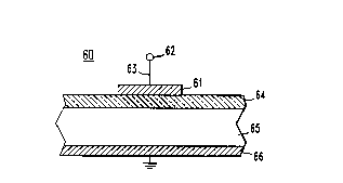
on exposed surfaces of electronic devices. Fig. 6 is a schematic representation of a field
effect device, 60, for inversion channel applications comprising means to apply a control
voltage or bias to a metal field plate 61 including electrical terminal 62 and conductor 63.
A dielectric thin film 64 comprises a uniform, homogeneous, dense, dielectric Ga2O3 layer
deposited ex situ or in situ by electron-beam evaporation of a single crystal, high purity
Gd3Ga5O,2 complex compound. The term in situ (in contrast to ex situ) characterizes the
deposition of said dielectric Ga2O3 thin film on a MBE grown semiconducting layer
without leaving the UHV environment. The method for depositing said dielectric Ga2O3
thin film is as described above and is as disclosed in the copending Canadian Application
Serial No. 2,136,581 filed November 24, 1994, titled Gallium Oxide Thin Films. The III-
V semiconductor 65 is of weak n-type or of weak p-type for p-inversion channel and n-
inversion channel applications, respectively. An Ohmic contact 66 completes the circuit.
The operation principles of such devices are well known from Si-MOSFET technology and
consequently, are not discussed in detail (see, for example, S.M. Sze, "Physics of
semiconductor devices", John Wiley & Sons, page 366, New York 1981).
In a particular example, the Ga2O3 thin films were ex situ deposited on bare n-type
GaAs substrates by said the above-described method of fabrication. The GaAs substrates
were maintained during deposition at 350~C with ~2 partial pressure of 2 x 10⁻⁴ Torr
in the evaporation chamber. The device was completed by fabricating Au/Ti dots 61 of
different diameters (50, 100, 200, 500 ~m) on top of Ga2O3 thin films 64 by evaporation
through a shadow mask and by providing an
..
2136580
g
Ohmic backside contact 66. High-frequency (1 MHz) capacitance voltage
~easurements revealed an unpinned Fermi level, excellent reproducibility of
flatband voltage and no detectable flatband voltage shift. Hysteresis was very small,
typically a few tens of millivolts or less. Fig. 7 is a plot of corresponding interface
5 state density vs. bandgap energy with substrate doping concentration of
1~6xl0l6cm-3 (Curve 71), and 8.6xl016cm-3 (Curve 72). Interface states Dit were
not detectable below midgap by high frequency measurements using Terman's
method
s
Dit (~I/so) = q2 dVs d~rs
_.EN
where C i is the capacitance of the dielectric layer per unit area, q is the unit charge,
V and V are the measured and calculated bias points, respectively, at the same
semiconductor surface potential ~s = ~IrsO7 i.e. at identical high frequency
capacitances (T.M. Terman, "An investigation of surface states at a silicon/silicon
15 o~ide interface employing metal-oxide-silicon diodes", Solid-State Elect., vol. 5,
page 285 (1962)). The resolution limit of this method is about 10l l cm-2 eV- l .
The midgap interface state density determined from Fig. 7 is below 10 12 cm- 2 eV~ l .
In another example, the Ga 2 0 3 thin films were ex situ deposited on
bare n-type GaO 5 In 0 5 P substrates by the above described method of fabrication.
20 The GaAs substrates were maintained during deposition at 125~C with ~2 partial
pressure of 2x10⁻⁴ Torr in the evaporation chamber. Specific resistivity, dielectric
constant and dc breakdown field of said Ga2O3 thin film are 4X10l2 Q cm, 10.2,
and 1.91 MV/cm. Frequency dispersion of capacitance was less than 5% below
midgap within the measurement range between 500 Hz and 1 MHz. Again, high-
25 frequency (1 MHz) capacitance voltage measurements revealed an unpinned Fermilevel, excellent reproducibility of flatband voltage and no detectable flatband voltage
shift. Hysteresis was very small, typically a few tens of millivolts or less. Fig. 8 is a
plot of corresponding interface state density vs. bandgap energy with substrate
doping concentration of 3xl0l6cm-3 (Curve 81), and 3xl0l7cm-3 (Curve 82). The
30 midgap interface state density is well below 101 l cm-2 eV- 1 and the interface state
density increases toward the valence band edge to values typically found at the
excellent Si/SiO2 interface.
~ ~121 36580
- 10 -
As demonstrated in both examples, the disclosed field effect device meets all
requirements such as unpinned Fermi level, very low density of interface states below
midgap (p-inversion channel), excellent reproducibility of flat band voltage, no detectable
flatband voltage shift, small hysteresis (typically a few tens of millivolts or less), and small
5 frequency dispersion of capacitance between 500 Hz and 1 MHz (less than 5%) for
inversion channel applications.
Further, Ga203 thin films deposited by said fabrication method are useful for
passivation of states on exposed surfaces of any kind of electronic III-V devices. The
interface recombination velocity is directly proportional to the midgap interface state
density. Since the demonstrated midgap interface state density is below 10~2cm~2eV~1 and
well below lO"cm~2eV~' at GaAs/Ga203 and GaO5InO5P/Ga203 interfaces, respectively, the
device performance and reliability are improved by small interface recombinationvelocities.
Various additional modifications will become appale-ll to those skilled in the art.
15 All such variations which basically rely on the teachings through which the invention has
advanced the art are properly considered within the scope of the invention.