Note: Descriptions are shown in the official language in which they were submitted.
2i371~
TITLE OF THE lNv~Nl~lON
High-voltage installation
BACKGROUND OF THE lNv~Nl~ION
Field of the Invention
The invention proceeds from a high-voltage
installation in accordance with the preamble of
claim 1.
Discussion of Background
High-voltage installations are known which have
a grounded metallic enclosure which is filled with an
insulating gas, for example SF6, and whose internal
surface situated opposite the high-voltage-carrying
active parts is provided with a protective coating.
This protective coating is to render this surface
smooth, inter alia so that it can be cleaned without
fibers or other residues of cleaning agents being
retained by surface roughnesses of the internal
surface, as a result of which the dielectric strength
of the insulating-gas gap would be reduced. The surface
of the active parts in such installations is often
provided with a similar protective layer.
The publication DE 41 20 309 A1 discloses a
high-voltage installation which has a metallic
enclosure which is filled with insulating gas and
surrounds the voltage-carrying active parts. Provided
on the internal surface of the enclosure as well as on
the external surface of the active parts is a
protective coating. In the case of this high-voltage
installation, a reduction in the dielectric strength of
the insulating-gas gap as a result of freely moving or
fixed particles can occur only to a limited extent
since the protective coatings are specially formed and
are at least partly coated with a second protective
coating. In such a high-voltage installation,
electrically conductive particles do not as a ,rule
move. Furthermore, the intensity of partial discharges
caused by particles is markedly reduced in comparison
with uncoated surfaces as a result of said coating.
2137 1 ~4
Free electrons, however, are not as a rule reliably
rendered harmless in this type of high-voltage
installation. The dielectric strength of the
insulating-gas gap could, however, be improved if
electrons which are produced in the vicinity of
surfaces as a result of partial discharges at peaks or
particles were captured. In addition, the application
of a second protective coating is comparatively
expensive.
SUMMARY OF THE lNv~N~l~loN
Accordingly, one object of the invention as
characterized in the independent claims is to provide a
high-voltage installation in which free electrons are
also reliably removed from the insulation gaps and in
which partial discharges generated by free particles
are reduced to noncritical values of intensity.
The advantages achieved by the invention are
essentially to be seen in the fact that free electrons,
which may, for example, be produced by switching
processes or by discharge processes, are absorbed by
the fullerene before they are able to initiate a
flashover.
The high-voltage installation has a metallic
enclosure which is filled with insulating gas and
surrounds voltage-carrying active parts. It has in
addition at least one partial coating either on the
internal surface of the enclosure or on the external
surface of the active parts, or at least one at least
partial protective coating both on thè internal surface
of the enclosure and on the external surface of the
active parts. The at least one protective coating is
doped with at least one fllllerene.
The protective coating can be formed as a layer
which is vapor-deposited directly on the appropriate
surface and composed of at least one fullerene.
However, the protective coating may also be applied to
the appropriate surface as a lacquer doped with at
least one fullerene, an epoxy lacquer or a lacquer
based on polyethylene being provided as lacquer.
21371~Q
-- 3 --
A particularly good action is produced if the
at least one fullerene is concentrated at the surface
of the lacquer or of the protective coating.
Preferably, C60 is used as the at least one
fullerene. Fullerenes having larger molecules may,
however, also be used.
The dependent claims relate to further
developments of the invention.
BRIEF DESCRIPTION OF THE DRAWINGS
A ~nore complete appreciation of the invention
and its further development and many of the attendant
advantages thereof will be readily obtained as the same
becomes better understood by reference to the following
detailed description when considered in connection with
the accompanying drawing, which shows only one method
of implementation, wherein:
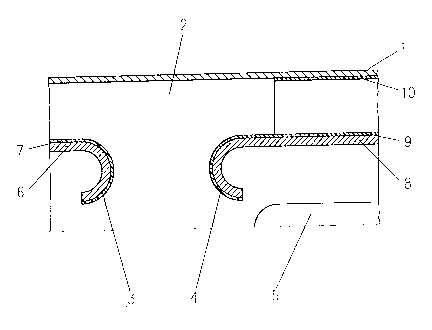
The sole figure shows a partial section through
a high-voltage installation according to the invention.
DESCRIPTION OF THE ~K~KKED EMBODIMENTS
Referring now to the drawing, the figure shows
a partial section through a high-voltage installation
according to the invention. An essentially
cylindrically constructed, pressure-proof metallic
enclosure 1 encloses an interior space 2 filled with
insulating gas, for example SF6. Disposed in the
centre of the enclosure 1 are active parts, of which,
however, only one switching point is shown in very
simplified form. On the one side of the switching
point only a screen 3 which concentrically surrounds a
fixed contact, which is not shown, is shown. Also not
shown are the contacts for the rated-current transfer,
which are situated inside the screen 3. Shown on the
other side of the switching point is a screen 4 which
concentrically surrounds a moving contact 5, which is
shown in the switched-off position. Here, again, the
contacts necessary for the rated-current transfer,
which are situated inside the screen 4, are not shown.
The switching point shown may be part of a circuit-
breaker or of an isolator or of a load interrupter
2137~ 04
-- 4 --
switch or of a grounding switch or a grounding
isolator .
The screen 3 is made of a metal sheet 6 which
is coated with a protective coating 7 on the side
facing the enclosure 1 and on the side facing the
oppositely situated screen 4. The screen 4 is made of
a metal sheet 8 which is coated with a protective
coating 9 on the side facing the enclosure 1 and on the
side facing the oppositely situated screen 3. The
internal surface of the enclosure 1 is also entirely or
partially coated with a protective coating 10. The
protective coatings 7, 9 and 10 comprise, as base
material, for example an epoxy lacquer into which
fullerenes, in this case C60 in particular, are
introduced. Lacquer based on polyethylene as base
material can also be used. The production of such
fullerenes is described in patent specification
US 5,227,038. In addition to such fullerenes,
conductive or semiconducting dopants, for example TiO2
components or conductively coated A123 or,
alternatively, a mixture of various substances, which
dopants are st~n~rd for such protective coatings, may
also be introduced. Still other electrically
conductive substances are also conceivable for
introduction into said coating. In each case, the
conductive protective coating renders the surface of
the part coated therewith similar to a surface which
acts as dielectrically smooth. Any fine peaks which
project slightly out of the surface no longer now have
a dielectrically harmful effect since they are situated
inside the electrically conductive or dielectrically
active protective coating.
It is possible to provide the internal surface
of the enclosure 1 and the external surface of the
active parts entirely with such protective coatings.
It may, however, also be expedient to provide said
protective coating in only one area or in a plurality
of areas of the high-voltage installation, and, to be
specific, particularly at those points where switching
21371~
gases-or other switching residues may occur. However,
for some applications it is also sufficient to provide
only the active parts with a protective coating, and,
to be specific, this may be done in one or more regions
of the high-voltage installation.
If the fullerene is concentrated at the surface
of the lacquer, thiæ results in a particularly high
efficiency of the fullerene. The fullerene C60 is
particularly suitable for use in high-voltage
installations because of its good receptivity for free
electrons. In addition, it can be produced
comparatively simply and is therefore particularly well
suited for a technical application. Fullerenes having
a number of carbon atoms higher than C60 can also be
used in this connection.
Fullerene layers which are vapor-deposited
directly on the appropriate surface and composed of at
least one fullerene may also be used as protective
coating 7, 9, 10. In this case, an adhesive based on
epoxy resin is often applied to the surface as
additional adhesive layer prior to the vapor deposition
of the fullerene. In this way, a particularly firm
joint is achieved between the fullerene molecules and
the appropriate surface. If a single-component
adhesive is used as adhesive, this results in a
particularly simple processing. The single-component
adhesive Araldite AV 119 of the CIBA-GEIGY company
(Araldite is a Registered Trade Mark of the CIBA-GEIGY
company) can be processed particularly simply since it
is thixotropic. Since the vapor deposition is carried
out at comparatively high temperatures, the single-
component adhesive Araldite AV 119 cures substantially
during this process. Should, however, the degree of
curing still be insufficient an additional curing must
be carried out in an oven.
In the production of said protective coating 7,
9, 10, the metallic surfaces are, as a rule, first
sand-blasted immediately before the application of the
single-component adhesive Araldite AV 119 as additional
21371~
-- 6 --
layer in order to achieve a good bonding of the
adhesive layer to the surface concerned. After sand-
blasting, the roughened surfaces are degreased
chemically with a grease solver such as acetone or
trichloroethylene. Thereafter, the single-component
adhesive Araldite AV 119 is then applied uniformly to
the degreased surface. The single-component adhesive
Araldite AV 119 is a formulated epoxy-resin adhesive
based on bisphenol A which can be processed easily and
without dripping.
It is possible that peaks which may be
conductive and which result in field distortions may be
present at the surface at the junction between the
surface and the adhesive layer. To smooth out such
field distortions, it may be expedient to dope the
single-component adhesive with a conductive or
semiconducting powder in order, in this way, to make
the adhesive layer into an equipotential surface with
whose aid a field distortion is avoided in this region.
In this way, it is possible to avoid with certainty
that partial discharges occur in this region.
To explain the mode of action, the sole figure
may now be considered somewhat more closely. If the
high-voltage installation is carrying voltage and if
the switching point is in the switched-off position, as
is shown diagrammatically in the figure, free electrons
are always generated by ionizing radiation and by
partial discharges initiated by freely moving or fixed
particles. Free electrons produced in this way may
generate further free electrons in avalanche fashion,
and, under unfavorable circumstances, if, for example,
the insulation has already been somewhat weakened as a
consequence of a previous overload, this may result in
a flashover between the active parts and the grounded
enclosure 1. Such flashovers are avoided with
considerable certainty if the free electrons are
already absorbed by the fullerenes present in the
protective coating 7, 9 and consequently rendered
harmless immediately after their production.
21371~
-- 7 --
If a conventional high-voltage installation is
systematically provided with these fullerene-contA;ning
protective coatings 7, 9, 10, the operational safety of
said high-voltage installation is thereby appreciably
increased.
However, if the previous safety margins are
considered as adequate, the dimensions of the high-
voltage installation provided with fullerene-contAining
protective coatings 7, 9, 10 can be markedly reduced
i0 with respect to the dimensions of an equivalent
conventional high-voltage installation, and this
entails appreciable economic advantages.
The fullerene-containing protective coatings 7,
9, 10 have an advantageous effect even if they are in
contact with gas clouds produced during switching
processes and contAining free electrons. They, or the
fullerenes, absorb said free electrons and thereby
accelerate, for example, the increase in the insulation
resistance between the screens 3 and 4 and,
consequently, also between the contacts of the
switching point. This accelerated dielectric recovery
of the switching point has the consequence that the
breaking capacity of said switching point is raised
somewhat, or its safety is increased.
Obviously, numerous modifications and
variations of the present invention are possible in
light of the above teachings. It is therefore to be
understood that within the scope of the appended
claims, the invention may be practiced otherwise than
as specifically described herein.
21371~4
-
-- 8 --
LIST OF DESIGNATIONS
1 Enclosure
2 Interior Space
3, 4 Screen
Contact
6 Metal sheet
7 Protective coating
8 Metal sheet
9, 10 Protective coating