Note: Descriptions are shown in the official language in which they were submitted.
WO 93/24316 ~ 1 3 7 2 8 8 PCI`/US93/05269
: ` "
DURABLE S_FACE COATINGS AND COATING PROCES S
Field of the Invention
The present invention pertains to thin, durable
surface coatings and processes for providing such coatin~s on
the surfaces of machine tools and the like.
Backqround of the Invention
Machine tools are required to perform a variety of
forming and material removal processes. For e~ample, such
tools are commonly used to repetitively perform cutting,
punching, chipping, milling, reaming, drilling, and other
functions. Dies are used commonly in forming and punching
operations. ~`
Tools wear constantly upon use and must be repaired
or replaced often depending upon the severity and frequency
of usage. In order to improve hardness, wear resistance, and
toughness properties, these tools may be surface coated with
a hard TiC, A1203, TiN, etc. layer. Coating methods vary
from Chemical Vapor Deposition (CVD) methods to arc plasma
spraying to various Physical Vapor Deposition Methods tPVD)
including sputtering and electron beam evaporation.
I Recently~TiN coatings on high speed steel tooling
have proven effective in improving tool hardness and wear
properties. TiN coatings are now commonly used on the
surfaces of gear cutters, gear-shaper cutters, drills,
SUBSTITUTE SHEET
~li3 i ~JV
W093/24316 PCT/US93/ ~ 9
reamers, taps, chasers, spade-drill blades, broaches, saw
blades and for other tools. These coatings are provided by
evaporative and sputtering methods in which atoms, ions
and~or neutral or charged clusters from a titanium source
(i.e., target) in a vacuum chamber are ejected onto ~he tools
that are positioned in the chamber proximate an anode. Inert `
gas such as argon is admitted to the evacuated chamber and,
upon creation of an electrical field in the chamber, serves
as a source of excited plasma ions which bombard the target
to dislodge the target (i.e., coating) material. Nitrogen is
also admitted into the evacuated chamber and serves as a
reactive gas which, along with the Ti materials ejected from
the target, forms the desired TiN coating on the tool. -
Typica~Ily, the process is a line-of-sight type operation in `
.
which the ejected Ti particles traverse the chamber in a ` ;
straight line, requiring rotation of the tools in the chamber ;
:
to provide a uniform coating thereover.
Although TiN surface coatings have provided ~ ;
significant improvement in machine tool life, there remains a
need to provide machine tool surface coatings which -
outperform TiN coatings in wear resistance and in heat -~
resistance. `~
Of further importance is the need to provide
improved coatings in a process in which the formation of
undesirable impurities such as carbon particles, sodium,
potassium and calcium, in the coating is inhibited. `~
,
, ~
SUBSTITUTE SHEET
W093~24316 2 1 3 7 2 8 8 PCT/US93/0~269
Additionally, there is a need to provide a
simplified coating process in which the need to rotate the -~
substrates during the process to attain coating uniformity is
eliminated.
Summary of the Invention
In accordance with the invention, hard, durable
titanium containing coatings are provided on the desired
substrate by a cathodic sputter coating process that is
operated under controlled process parameters. Briefly, the
desired substrates, such as tools, airfoîls, turbine blades,
etc. are loaded onto a stationary jig that is placed within
the sputter chamber.
Three electrode cathodic sputtering is conducted in
the chamber with a biasing electrode provided as the third ~;;
elec~rode. A titanium alloy target, as explained in more
detail hereinafter, is positioned in the chamber and serves
as the cathode. The target substantially surrounds the
substrates in the chamber. In accordance with conventional
cathodic sputtering techniques, the stationary jig and
associated substrates are charged as the anode, with a
potential difference of from about 500-lOOOV e~isting between
target cathode and anodic substrate. The chamber is
evacuated to vacuum pressure of between about 10~l Torr. to
10-3 Torr.
SUBSTITUTE SHEET
WO93/24316 ~ 3 ~ ~ 8 PCT/US93/~6
- 4 -
An inert gas, pre~erably argon or ~enon, is backfilled into
the evacuated chamber to serve as a source for formation of
e~cited plasma ions upon creation of an electrical field in
the chamber. These ions, in accord with conventional
sputtering techniques, strike the target to dislodge atomic
or molecular coating species therefrom.
In an especially unique aspect of the invention,
both nitrogen and oxygen are admitted into the chamber -
substantially concurrently to serve as reactive gases for
formation of the desired coating on the anodic substrates,
this being done in a non-magnatron DC sputter system. In -
contrast, conventional coating processes use only one or the `;
other of these elements to form a coating on the desired -~
substrate ~ref. U.S. Pat. Nos. 4,714,660; 4,871,434 and ;~
4,973,338).
ImproYed sputtering also results from a biasing
electrode whose potential is maintained at from -22 to -23V
relative to the anodic substrates. Although applicant is not
to be bound to any particular theory of operation, it is
thought that the electrical field between the anode and less
positively charged biasing electrode provides for a-second or
"mini" sputtering in the assembly in which impurities, such
as c'arbon particles, sodium, potassium and calcium which
would otherwise incorporate into the coating, will eject from
the anode and migrate to the bias electrode.
. ~ .
~.~
SUBSTITUTE SHEET `~
'.
W093/24316 ~ 1 3 7 X ~ 8 PCT/US93/~5269
;~......
- 5 -
The invention will be further described in
conjunction with the appended drawings and detailed
description.
Description of the ~rawinqs
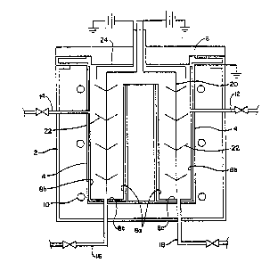
Fig. l is a schematic sectional diagram of a
three-electrode sputtering chamber used in accordance with
the invention;
Fig. 2 is a schematic depiction of the anode and
biasing electrode of the sputtering chamber; and
Fig. 3 is a cross-sectional view of a substrate ~ ;
coated in accordance with the invention.
Detailed DescriPtion of the Preferred Embodiment
Turning now to the drawings and specifically to Fig. -
l thereof, there is shown a sputter ion plating assembly 2.
Assembly 2 is preferably Model GLO-TINE 24X36 Abar-Ibsen,
from Abar-Ibsen Company but could also be any other
commercially available ionic sputter chamber assembly
provided it is capable of achieving or can be modified to
attain the sputter coating process parameters that are
detailed herein. Assembly 2 comprises a vacuum vessel 4 and
lid 6 which together provide a sealed environment within for
provision of viacuum conditions necessary for the sputtering
operation. A Cathodic target 8a, 8b, 8c is provided in the
assembly and, as shown, is shaped to substantially surround ~,`;
SUBSTITUTE SHEET
W093/24316 ~1 3 7 2 8 8 PCT/US93/U~9
- 6 - ~
substrates 22 that are disposed on stationary mount 20 fitted
through lid 6 of the assembly. The cathodic target comprises
relati~ely spaced apart inner and outer cylindrical wafl
liners 8a and 8b, respectively, and a circular bottom wall
liner 8c, all formed from titanium alloy, as described ;~
below. The inner cylinder 8a is placed on the bottom wall ~;-
liner 8c in the center of the outer cylinder liner 8b which
is closely surrounded by the vacuum vessel 4. The spacing of
the cylinders from each other is dependent on the size of the
substrate to be deposited and is arranged to form a circular
opposing cathode and to maintain the substrate in the middle
of the negative glow region of the glow discharge and not in ~-
the cathode-fall region.
Heating elements 10 are provided for heating the ~`~
gaseous environment, thereby suppressing homogeneous
nucleation of particles of the material in the gaseous
environment. Homogeneous nucleation occurs readily at hiqh
concentrations of vapor species within an ambient gaseous ~`
environment and is to be avoided, as disclosed in U.S. Pat.
No. 4,236,994. Its occurrence gives the deposited material a ~'t'~
porous, friable and columnar structure characteristic. Y;`
Cooling fans (not shown) or other equivalent means are used
to cool the vessel. Biasing electrode 24 is positioned`above
mount 20.
Vacuum connection 12 communicates with the interior
of assembly 2 to provide the vacuum conditions required for
SUBSTITUTE SHEET ~;`
.,
W093/24316 PCT/US93/0i269
`i `~'~37~8~ :~
- 7 -
the coating operation. Gas lines 16 and 18 provide a source
for entry of the desired inert gas, preferably argon, that is
necessary to form the e~cited ion plasma cloud necessary for
sputter coating. Gas lines 16 and 18 also serve as entry
ports for the reactive gases, oxygen and nitrogen,
respectively. Alternatively, a common entry port for all
three gases could readily be provided.
The assembly is operated as a three-electrode
sputter coating apparatus in which the target 2 serves as the
cathode, with the mount 20 and associated substrate 22
charged with a positive D.C. current of from about +500 -
+lOOOV to serve as the anod~. I have found that maintenance
of biasing electrode 24 at from -22 to -23V less than the
voltage of anode mount 20 provides enhanced coating in that
impurities which may otherwise coat onto the substrate are
not normally formed thereon. A potential difference of
-22.6V is most preferred. Further, use of the biasing
electrode tends to provide increased toughness micronodular `
coating structures compared to unbiased coatings. The target
8 is preferably maintained at ground but a negative voltage -
potential could also be imparted thereto. -
In accordance with the invention, target 8 is
composed of either Ti-6 Al-4V alloy or Ti-8 Al-l Mo-lV
alloy. The former alloy is presently preferred based on
preliminary testing. Both of these alloys can be purchased
SUBSTITU~E SHEEl
2 1 3 7 2 8 8 ` P~T~US93/~-~69 ~
from a variety of sources, including Titanium Alloys,
Pittsburgh, PA. The target materials are rolled and machined
into the desired shape for use as targets 8 in the assembly. -~
Workpieces or substrates 22 are preferably cleaned
prior to operation of the sputtering coating process. In ~-
this regard, any one or more conventional cleaning processes, ~-`
includinq alkaline cleaning, electrolytic cleaning, emulsion
cleaning, solvent cleaning, acid cleaning, pickling, abrasive
blast cleaning and salt bath descaling can be employed.
! " ~ ` .
The cleaned substrates 22 are then loaded onto the `-
stationary mount 20 that serves as an anode in the process.
One surprising aspect of the invention is that adequate throw
or carry of the coating material is provided such that the
coating will substantially uniformly coat over the substrate
" ,~:
without requirement of rotating the substrates 22.
A vacuum of from about 10~1 to 10-3 Torr. is
provided in the enclosure. Preferably, a vacuum of 10-
~
Torr. is provided. This low pressure or ~soft" vacuum is ~`~
thought primarily responsible for the aforementioned
e~cellent ~throwU or carry of the sputtered coating ` -~
particles. The envelopment of the substrates by the target
also aids in this phenomenon.
`I During sputtering, argon is fed to the assembly
within a range of from 300-460 SCCM, with 425 SCCM being a '
preferred feed rate. Initially, nitrogen is fed to the
', .
.
: '
SUBSTlTUTE SHEET
. WO93/24316 ~ 3 7 2 8 8 PCT/US93/05269
.
enclosure with oxygen feed commencing within about 1/2 hour
and continuing concurrently with the nitrogen feed~ The
nitrogen is fed to the enclosure within a range of about 12.5
to 13.5 SCCM with o~ygen feed rates being maintained at from
about 10 to 14 SCCM. The molar ratio of ogygen:nitrogen fed
into the enclosure may range from about 1:1 to about 1.25:~. -
Preferably, the two reactive gases are both fed at 13.1 SCCM
resulting in a slight molar excess of o~ygen relative to
nitrogen. The sputtering process proceeds for about 5-8
hours. ~.
The sputtered coatings of the invention show
significant improvement over prior art TiN coatings in regard
to.heat and wear r.esistance of cutting tools coated thereby.
Accordingly, at present, the processes and coatings.of the
invention are used to coat toolings and other parts in which :~
heat, abrasion and shear resistance are important. The
substrates 22 can be composed of a plurality of different
metals ranging from a wide variety of steels, stainless
steelsj titaniums, carbides and inconel-type alloys and
ceramics such as A12O3, SiN and SiO2. Although the
substrates are preferably to be used ultimately as machine ~
tooling products, including dies and gears, other substrates
thatlmay be beneficially coated in accordance with the
invention include turbine blades, airfoils, etc.
SUBSTITUTE SHEET
`~ :
WQ93~24316 PCT/US93/~P--~69 ::
~137288
1o - : :~
The preferred Ti-6 Al-4V alloy target has the ~:~
following composition. ~:
N .012 (percentages given by weight)
C ~ O 1
O ~ 12E3 ~ s
Fe .18
Ti 90.06 "~
Al 5.9
V 3.7 .~:
H 80 ppm ~.`
Y less than 50 ppm `~:
As to the Ti-8 Al-l Mo-lV target material~ this has ~.
the following composition:
N .015
C . 01 - ' ~,
O .125 :
H .125
Ti 89.175
Al 8.0
V 1.25
Mo 1.25
When the above target materials are sputtered in .
conjunction with the conjoint use of both N2 and 2 as
reactive gases, thin, durable coatings on the order of 2.0 x
10-5 to 8.0 x 10⁻⁵ inches in thickness are formed. In fact,
::.
pxeliminary results in connection with one test run indicate i.
that the coating thickness was 6.5 x 10⁻⁵. .
Coatings resulting from sputter coating with the .j
above targets and reactive gases may be described as
including the elements Ti, Al, V, Y, O and N, with Mo also :
being present when the Ti-8 Al-l Mo-lV target material is `:
used. ;~
'.'.:'
' ::
SUBSTITUTE SHFET ;
WO93/24316 ~,1 3 7 2 8 8 PCT/US93/0~269 ~
- 1 1 - , ;
When the preferred Ti-6 Al-4V target is used, Ti,
Al, and V are present in o~ide or nitride form. The formula
Ti v AlO2N is used for simplification. Similarly, when the
Ti-8 Al-l Mo-lV target is used, Ti, Al, and Mo are present in
o~ide or nitride form. The formula Ti V Mo AlO2N is used for
simplification.
Turning now to Fi~. 2, there is schematically shown
substrate 22 and ~ias electrode 24 during sputtering. Since
the bias electrode 24 is maintained at from -22 to -23V
lesser potential than the substrate ~e.g., anode) 22, a -
Umini'' or second sputtering causes the e~cited Ar plasma to
impinge upon substrate 22, dislodging impurities, such as C,
Na, K, and Ca therefrom and provides a dense equia~ nodular
microstructure.
Fig. 3 illustrates substrate 22, here shown as a
drill bit, coated on its surface, with a uniform thin, layer
of coating 26 thereover. Coating 26 has a thickness of from
2.0 x 10⁻⁵ to 8.0 x 10⁻⁵ inches.
The following table is illustrative of the increased
longevity of tools coated with the above-described Ti V AlO2N
material over identical tools coated with a conventional TiN
material.
TOOL I WORK MATERIAL PIECES MACHINED
OR OPE~ATIONS PERFORMED
BEEORE RESHARPENING
TiN Ti V AlO2N
CO~T _ COAT
INSERT CAST IRON 134 402 ~`
(TNMG-432)
~UBS~ITU~E 8HEE~
W093/24316 ~1 37 2 8 8 PCT/US93/0~69
- 12 -
INSERT 4140 105 1029
(TNMG-432A)
MILL CAST IRON 35 156
CUTTER
SHAPER CAST IRON 39 1~1
CUTTER ~
END MILLS 4140 100 175 `.
~3/16")
INSERT CAST IRON 150 1817 `~
(VNMP-33lA) ` ~ ~ ;
INSERT STAINLESS STEEL 150 240
(ROUND) ` `
HOBB 8620 3Q 120 `~
DRILL ` 86`20 175 800: .
~TAP : ~ 1018 Rod 1500 10, 870
20 OSG)~
While~tbis~invention has been described with respect
`to pa ~i~cul:a~r;embodiments thereof, it is apparent that .~
numerous~othe~r~forms and modifications of the invention will '.'`'`
bè obvious to those skilled in the art. The appended claims !~
~and~ this invention~gener~all:y~should be construed to cover all
,such~obvio:us~`forms~ and~modifications which are within the ,`~,`,'
8pir~i,t and;~scope~o:~the~invent~ion. ~ ~ : -'`.,;
'1'`,`' .
~ ~ . .... ~,.
" ..,
SUBSTITUTE SHEET i ^`
. - . .