Note: Descriptions are shown in the official language in which they were submitted.
94/00807 ~ ~ 3 7 ~ 6 3 Pcr~ys~3~047~7
MO~
FIELD~2E~VENTION
-i The present invention relates generally to the field of con~olling
5 induction motors, and more particularly to ~n apparatus for conserving energy in
opera~ing induction motors.
~ .
The use of A(: induction motors has become commonplace. Many
ordinary appliances and much of the equipment used in residen~ial as well as in
10 industrial and commercial settings utilize such motors. The motors ar~ ordinarily
connected to power lines provided by local utility companies, which can vary
substanaally in voltage between locales and over time. lnduction motors typically
operate at relath~ely constant speeds, the speed being independent of the applied
AC voltage to the motor over a ran~e of opera~ing vol~ages.
Unfortunately, induction motors udlize`significant power when
operating without a load. Specifically, dle current drawn by the motor is generally
constant, and depends on the voltage applied to the motor. Therefore, it would be
desirable to decrease the voltage to dle motor when d~e motor is not loaded,
thereby decreasing energy used by the motor. However, most motors are operated
20 by line vol~es that are not adjust~ble by ~e user. Even where volta~e may be
;: adjusted, it is difficult ~o make the necessary adjustments to quickly respond to
chan~es in load.
The energy consumption of an induction motor is determined from
the inte~ral over a predetermined period of the product of the instant~neous AC
25! voltage applied across the motor terminals and the instantaneous AC current
throu~h ~e motor. Typical AC line volta~es are sinusoidal. It is known that
applyin~ a sinusoidal input to an induction motor will result in both the AC volta~e
and AC current havin~ the same sine wave shape but off~et in time. The time
offset between volta~e and current is called a phase shift or phase difference and is
30 typically expressed as an an~le. For a constant volta~e and. hence, relatively
constant culTent, the power consumed by an induction motor may be expressed as
Vlcos~, where V is the avera~e value of the applied AC volta~e across the motor, I
w094/00807 ~ 3'1365 PCr/~S93/M797 ~ ~
is the average value of ~he A(: current through the motor and ~ is the phase
difference between the voltage and the current. Cos ~ is sometimes refelTed to as
the "power factor". Thus, power consumphon i related to the phase difference
between ~e AC voltage applied to the motor and the A5~ current dlrough the
5 motor. It is well known that ~e phase difference between the voltage and cuIrent
in an induction motor and, therefore, power consumption changes with changes in
ehe load applied to ~e motor. However, when the motor is unloaded the power
factor remains large enough to result in substantial wasted energy due to the
relatively lar~e cu~ent which flows through the motor. While it may, in theory, be
10 possi~le to maximize the efficiency of an induction motor which is subject to a
constani load, many, if not most, applications for such motors involve loads which
vary over time.
One method for reducing the energy consumption of an induction
motor utilized in the prior art will be referred ~o as Power Factor Control or PFC.
-~ . ~
`~ 15 By measuring chan~es in the phase difference between the volta~e and current,
chan~es in power consump~ion and, thus, in applied load may be detected. This
prior art method of PFC involves measuring the phase difference` between the
volta~e and current and u~ing this measured information to interrupt the application
of line voltage to the motor for a por~ion of each AC cycle. By varying the
20 duration of the interruptions of the AC voltage in response to chan~es in the phase
difference between the current and the voltage it is possible to adjust the rms (root
- mean square) value of the ~pplied volta~e. Thus, when the motor is lightly loaded,
i.e., ~ is large, the nns voltage is reduced. On the other hand, when the motor is
~ully loaded, i.e., q~ is small, the rms voltage is increased, i.e., the interrup~ions of
25 the line voltage applied to the motor are minimized or eliminated.
An exarnple of an apparatus utilizing this PFC approach is disclosed
by Nola in U.S. Patent No. 4,052,648. Nola teaches measurin~ the phase
difference between current and volta~e and using the measured information to
control the duration of the voltage to an induction motor by means of a triac. A30 triac is a well known device controlled by a gate whîch can act tO interrupt voltage
applied to the motor. Nola measures the voltage applied across the motor by
means of a center tap transformer whose primary coil is connected in parallel with
WO 94/00807 ~ 1 3 7 3 6 ~ PCI/U~93/~47~7
the motor. The center tap transformer produces two oppositely phased voltage
signals from the tenninals of its secondary. These two volta~es signals are thenpassed through a square wave shaper, which is at a uniform high value when AC
voltage is positive and is uniformly low when AC voltage is nega~ive. This
S shaping removes all amplitude information while maintaining polarity informa~ion.
Simul~neously, the current is detected by a second ~ransformer, the
outpu~ of which is also passed dlrough a square wave shaper. The square wave
ou~ut is then differentiated, creating a series of spikes which indicate momentswhen the current switches direc~ion and is therefore at zero. These points are
10 referred to as zero point crossings. These spikes are fed into a one-shot ci~cuit,
which generates a square wave output. Next, the volta~e square wave and the
current square wave are multiplied. The resulting ~ctangular wave consists of
pulses wi~ a width related to the phase difference between the cunent and vol~age
~ squarewaves. l his signal is then integrated, and the ou~ut is monitored. If the
- 15 load decreases, the phase angle between the current and voltage changes, and the
pulse width then changes. Such changes cause the gate control circuit to disengage
the tnac for a longer portion of each AC cycle, decreasing the rms voltage applied
to ~e motor and energy consumption.
It is believed ~hat the apparatus described has not performed well in
20 pracdce and has not been commercially successful. The probable explanation for
these problems is the complexity of the apparatus. While numerous attempts have
- been made to diminish this c~mplexity, no prior art Power Fac~or Control system
' known to the inventor has overcome these problems.
An example of an attempt to overeome the complexity of the
~5 1 apparatus described in the '648 palent is set forth by Nola in U.S. Patent No.
4,266,177. In this second patent, Nola teaches a system which also relies on
monitorin~ the phase difference between the voltage and current using different
circuitry. Nola's second approach includes generating first and second square wave
signals from the AC operating voltage across the motor leads and from the current
30 passing through the motor, respectively. These square wave signals are then
summed and integrated to ~enerate a si~nal which is transmitted to the non-
inver~in~ inpu~ of an operational amplifier. The edges of these signals are also
W O 94/00807 t~3136~ P(~r/US93/04797
detected and are used to ~ime a ramp generator. The output of the ramp ~eneratoris transmitted to the inverting input of that same operational amplifier. The output
of the operational ampli~ler is the difference between the average value of the
sumrned signal and the value from the ramp generator. The phase difference
S be~ween current and voltage is measured by the widtk of the surmned signal.
Wider pulses yield larger integrated outputs, which are then transmitted to the
operational amplifier. Therefore, an increase in the phase difference will result in a
larger differenee signal from the operational arnplifier. This difference signal is
used to con~rol a tria~ which con~ols AC voltage to ~he motor.
This apparatus continues to rely upon removing magnitude
infom~ation from the detected voltage and current signals, and requires complex
circuitry to accomplish control of the applied motor voltage. Again, it is believed
that the apparatus described in the '177 patent has not enjoyed commercial success.
Most inducdon motors are designed to operate adequately at
I5 predetermined line voltages. Normally, the motor designer must assume that the
motor will be operated at the lowest line voltage no~nally encountered. Such a
voltage may be far lower that the normal line voltage available at most locations
and at most times. For example, a motor used in a refrigerator must be capable of
ddivering adequate power under full load during a "brown-out" condition, i.e.,
20 when a udli~y reduces line volta~e over its entire gnd (or portion thereof) in
response to unusually hi~h elec~rical energy demand. Chan~es in line voltage
affect both motor performance and energy consumption. Wide variations in line
volta~e are undesirable. Unfortunately, such variations are beyond the control of
- most motor designers and users. It is noted that ordinary line voltage fluctuations
25 will not result in chan~es in the phase between the current and the voltage.
Therefore, prior art PFC systems will not respond to fluctuations in line voltage.
Thcrefore, there is a need for a energy savin~s system for controllin~
the voltage applied to an induction motor which is simple, which is responsive to
chan~es in line voltage to adjust for such changes, and which is responsive to
30 changes in motor loading to adjust for such changes.
According!y, it is an object of the present invention to provide an
improved induction motor control system for energy savin~s.
WO 94/00807 ~v 1 3 7 3 ~ 5 PCr/lJS93/04797
Another object of the invention is to provide an energy savings
system for use wi~h induction motors which are simpler in design than ~he prior
. ~
These and other o~ects of the inven~on will become apparent to
, S those skilled in ~he art from the following descnption and accompanying claims
and drawings.
The present invention comprises an apparatus and method for
~ con~olling the voltage applied to an induction motor. The method includes
10 receiving an AC line voltage. An operating AC voltage is generated from the AC
line voltage and this operating AC voltage is applied across the motor. A first
signal, which is a func~ion of the magni~ude of the operatmg AC voltage, is
gener,ated and a second signaL which is,representative of the magnitude of the AC
culTent ~rough dle motor~ is also generated. A compositç signal representative of
15 a combinadon of ~he f~t and the s~ond signals is then generated. The composite
, ~ ,'~ ` signal is then averaged to generate an average signal representative of the average
.. ~ , -
value of dle composite signa~. The operating AC voltage is continually readjusted
- in response ~ changes in d e average signal.
, ~ An apparatus implementing dle method of the present inven~ion is
,~ 20 also taught. The apparatus încludes ~erminal means for receivin~ an AC line
voltagej means for generating an operating AC volta~e from the AC line voltage,
connector means for applying the opera~ng AC ~olta~e across the motor, voltage
, ~ ~, detection means for ~eneratin~ a first signal which is a function of the magnitude
-~ ~ ~ of said operating AC voltage, and current sensin~ means fQr generating a second
~, , , 2S signal rep,resen~ati~e of the magnit;ude of the AC current throu~h the rnotor. ~Si~nal
combinin~ means are provided for generating a composite si~nal representative of a
combination of the first and the second signals, as well as signal averagin~ means
~ .; ~ . .
for generatin~ an average signal representative of the avera~e value of the
~- composite signal. Finally, the apparatus includes AC voltage modulation means for
~- ~ 30 adjusting the operating AC volta~e in response to the average si~nal.
~, In the preferred embodiment of the apparatus of the present
invention, the AC volta~e modulation means comprises volta~e reduetion means for
W094/oo8o7 ~ 36a PCr/U593/04797
switching off the line voltage for a por~ion of each cycle, the length of the por~ion
being determined by the average value of the composite signal. The voltage
modula~ion means may comprise a phase control integrated circuil device f~r
controlling a triac. The phase control integrated circuit device is responsive to the
S average signal to generate a control signal operative to control a ~iac to switch off
~ansmission of the line voltage to the motor for ~he portion of each cycle.
BRlEF DESCRlPl`lON OF THE DRAWINGS
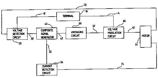
FIG. 1 is a block diagram showing the major funcional components
comprising the present invention.
FIG. 2 illustrates an AC volta~e modulation means 60 of FIG. 1.
PIG. 3 illus~ates an preferred implementa~ion of voll:age detection
circuit 20 of FIG. 1.
FIG. 4 illus~tes a preferred implementation of culTe,nt sensing
circuit 30 of FIG. 1.
FIG. S illustrates a prefe~ed implementation of composite si~nal
~enerator 40 and of averagin$ circuit 50 of ~IG. 1.
DETAlLED DESCRlPTION OF THE II~ENTION
While it is well-known that adjusting the voltage applied to an
induction motor depending on the load rnay be used to save energy, in order to be
20 practical for most applications, volta~e adjustment means must be able to quickly
respond to chan~es in the motor load. Available technologies for sensin~ such
changes have not proved practical for widespread application. In this regard, there
is a need for a relatively simple, inexpensive, "foolproof" yet reliable energy saving
device.
; ~ ~ 25 The present invention employs novel means for sensin~ chan~es in
the loading of an ac induction motor and thereby allowing adjustr,nent of the
volt~e to the motor to save energy. Previous ~,fforts at sensin~ variations in the
loading of an AC induc~ion motor have focused upon measurement of the phase
difference between the motor voltage and motor current. Measuring this phase
30 dif~erence required complex circuitry. The task was fur~her complicated by the fact
that the voltage (and culTent) to the motor were bein~ interrupted during a portion
of each cycle. The apparatus of the present invention does not rely on
..... ... , .. ...... .,.. . ,.;~ .. .... . . . . .
A~O 94/00807 2 1 3 7 3 5 S
measurement of phase difference. lnstead, load sensing is accomplished by
monitonng the current through the motor, and measuring changes in a composite
signal denved from this culTent and the voltage applied acr~ss the moeor. This
approarh is somewhat contrary to the conventional ~,visdom in that, for a given
voltage, the magnitude of the current through an induction motor is believed not to
vary and that only the phase difference changes. Hence the conventional approachteaches ~at voltage and current rna~nitude information are unimportant and that
only phase tirning information is useful in detennining the load status of ~e motor.
By contrast, the present invention utilizes this magnitude information which is
10 disregarded in the prior art to determine changes in the load status of the motor.
In another aspect of the present invention, the ma~nitude of the
-volta~e applied to the motor, called the "opera~in~ voltage", is held constant (for a
given load) notwithstanding fluctuations in the line voltage.
, ~ ~
A motor controller circuit according to the present invention contains
15 t he subcircuits illustrated in block diagram form in ~IG. 1. The overall circuit
combînes two f~edback loops~ ln the~first loop the operating AC volta~e across amotor 70 is detected by voltage detection circuit 20, which generates a first voltage
signal representatîve of the înstantaneous ma~nitude of the voltage applîed to the
motor. In the second feedback loop, thc current passin~ through motor 70 is
20 detected by current detection cîrcuit 30, which ~enerates a second voltage si`gnal
representative of the instantaneous magnitude of the cDnt through motor 70. The
first and second instantaneoùs voltage signals are then combined in composite
signal gen~rator 40 to generate a composite instantaneous signal, which is time
averaged in averaging cîrcuit 50 to generate an volta~e si~nal representing the
i25 value of the composite si~nal over at least onè complete cycle. This avera~e si~nal
controls a voltage modulation circuit 60, which intelTupts application of the ACline volta~e to motor 70, thus controllin~ the ma~nitude of the operating AC
volta~e applied to the motor. Volta~e feedback to volta~e modulation circuit 60
~, responds both to changes in load and to changes in the operating and line volta~es.
More speci~lcally, a tenninal 10 is provided for directly receivin~ an
AC line volta~e from an AC power supply system (not shown), for example, an
ordinary AC outlet. Volta~e modulation circuit 60 receives the AC line volta~e
wOs4~0o~o7 ~ PCI/US93/04797
from tem~inal lO via AC voltage connector 14. Vvltage modulation circuit 60
modulates ~e AC line voltage to ~enerate the operating AC voltage applied to themotor. llle AC line voltage is modulated so that the power transmitted to motor
70 via modula~ed AC voltage connector 62 varies in response to a control signal
S received by voltage modulation circuit 60 from average signal connector ~2. The
medlod by which the "average" signal is generated is discussed in detail below. It
is important to note that the circuit according to the present invçntion is utilized in
connection with an induction motor 70 which is part of a separate device apart
from the motor controller. It is included in the Figures and discussion herein to
10 clarify the relationship between the motor controller circuit and motor 70 to be
controlled.
The average signal, which con~ols voltage modulatlon circuit 60, is
~enerated by combining two si~nals. The ~st signal is generated from the voltageapplied across motor 70 by transmitting the operating AC volta~e across applied
15 AC vol~e connector 72 to voltage detection circuit 20 Voltage detection circuit
20 generates dle first signal, which is a function of the magnitude of the operating
AC voltage. In the preferred embodiment of the present invention, this
representation is a difference signal between the AC line voltage and the operating
AC voltage. Hence a difference signal between the AC line voltage received over
¦- 20 AC line voltage connector 12 and the operating voltage received over operatin~ AC
volta~e connector 72 is generated and rectified. Those skilled in the art will
recognize that a variety of a~terinative output signals may be generated which are
also functions of the operatin~ AC voltage.
J The second signal, representative of the ma~nitude of the cuIrent
~, f 25 throu~h ~e motor, is generated as follows. The current passin~ throu~h motor 70
is measured from current signal connector 74 by current sensin~ circuit 30.
Current sensin~ circuit 30 ~enerates a second volta~e si~nal by sensin~ the current
passin~ through the motor and ~eneratin~ a volta~e si~nal representative of the
ma~nitude of the current passin~ throu~h the motor. ln the preferred embodiment
3Q of the present invention, the motor current sensed by current sensin~ means is
rectified by current sensin~ circuit 30. It will be obvious to those skilled in the art
~VO94/00807 ~ 6S Pcr/us93/04797
~at a variety of output si~nals may be ~enesated which are ulso representa~ve ofthe culTent passing throu~h motor 70.
- The composite signal is generated by composite signal generator 40
from the f~st sig,n~, which is obtained via ~Irst signal connector 22, and from the
S second signaL which is obtained via second signal eonnector 32. The resulting
eomposite signal is then transmitted Yia composite signal connector 42 to averaging
circuit 50. Averaging eircuit 50 averages the instantaneous value of the composite
signal over at least one cycle, to generate a voltage representative of the timeaverage of that AC voltage.
In the preferred embodiment of the present invention, the composite
signal is obtained by combining the two voltage si~nals by means of a resistive
volta~e divider circuit located within composite si~nal ~enerator 40. The preferred
~: embodiment also includes an integrator cir~uit located within averaging circuit 50
to obtain the average si~nal from the eomposite signal. The avera~e signal thus
15 generated is a si~nal representative of the rms value of the sum of the first and
second signals. which themselves are related to the magnitudes of the volta~e
`~ across the motor and the ~urrent through the motor, respectively.
:~
: :
One prefe~ed embodiment of an AC vol~e modulation circuit 60
20 of FIG. 1 according to the present invention is illustrated in FIG. 2. Elemènts
- ~ ~ illustrated in FIG. 1 present in FIG. 2 - ~ are labelled consistently throu~hout. In
: :
-~ ~ this subcircuit a phase control chip 110 responds to the si~nal from average si~nal
-~ ~ ~ connector 52 to control pilot triac 112 and thereby main triac 114. Main triac 114
acts to interrupt application of the AC line volta~e to motor 70 and thereby
25 ~enerate the operating AC voltage.
The AC line voltage is received at AC volta~e modulation circuit 60
via unmodulated AC volta~e connector lines 14, includin~ an AC line volta~e line("AC hot") and an AC neutral line.
, Modulation of the AC operatin~ volta~e of the preferr~d
¦ 30 embodiment of the present invention is accomplished usin~ pilot triac 112 and
main triac 114. A triac is a well known device whereby small culTent si~nals
applied to its ~ate can control much lar~er current flows at much hi~her volta~es.
... . .. .... .. - . . . .; . -. . ~ -
W094/00807 ?,~,~V136~ PCI/I~S93/04797
A triac is triggered into conduction by pulses at its ~ate. In ~e present circuit a
signal applied at the gate of pilot triac 112 from phase con~ol chip 110 permits a
cu~ent to flow through triac pilot 112, which is applied tO the gate of main triac
114. While it might be possible for a single stage triac to be utilized, a two sta~e
triac arrangement allows for control of the relatively lar~e current to a high power
motor by a phase control chip which has only a limited capacity to deliver a gate
con~ol current. Therefore, this sta~ed triac arrangement permits the output of
phase con~ol chip 110 to con~ol the applied AC voltage to motor 70 over
modulated AC voltage connector 62.
The voltage applied to the motor is controlled by the control signal
pulses received at the ~ate of pilot triac 112 from phase control chip 110. In one
embodiment of the present invention, a TDA 2088 phase controller chip from
Plessey Semiconductors is utilized as phase control chip 110. The TDA 2088 chip
is designed for use with tnacs for use in current feedback applications, and is
15 ~requently used~ for speed con~ol of small universal mo~ors.
Phase control chip llO requires an a~plied Yolta~e at voltage input
pin 132 of -12 V and a 0 V reference voltage at 0 V reference pin 142. These
voltages are used to power the chip and to generate a -5 V reference voltae at -5
V reference pin 124. This voltage is obtained from the AC line volta~e by a
20 power supply subcircuit, which opera~es as follows. Resistor 164 and capacitor
162 are connected in series to the AC line voltae on AC line hot line 14 to
provide a filte^red voltage to diodes 160 and 1~8, which pe~nit only the negative
half cycle of the AC line voltage to pass. Capacitor 178 is provided to smooth the
resulting volta~e at volta~e input pin 132, and zener diode 180 latches the volta~e
2~ at that pin to a value of -12 V.
Phase control chip 110 supplies control si~nal pulses at triac gate
output pin 134. Phase control chip 110 has an internal ramp generator whose value
', is compared to the voltage applied at pro~ram input pin 122. When these two
values are equal an output pulse is triggered. The ramp generator has two input
30 connections. First, pulse ~iming resistor input pin 126 is connected to a -5 V
reference by pulse timin~ resistor 152. Secondly, pulse timin~ capacitor input pin
144 is connected to ~round by pulse timin~ capacilor 148. The values of pulse
~VO 94~0807 ~ 1 3 7 3 6 ~ Pcr/vsg3/o47g7
11
timin~ resistor 152 and pulse tirning capacitor 148 are chosen to define the slope of
the ramp si~nal.
In addi~ion to the support cir~uitry for phase control chip 110
described above, AC voltage modulation circuit 60 is provided with a therrnal
S switch 150. Thermal swi~ch 150 is connected between ground and avera~e signal
connector 529 which applies the ~verage si~nal frorn avera~ing circuit 50 to
program input pin 1'~2 of phase con~ol chip 110. Thermal switch 150 acts to
ground out program input pin 122 if ~he system overheats. This is a safety feature
which acts to shut off the motor in the event of cir~uit overheating.
-- Also, resistor 174 and capacitor 176 are provided to act as a
"snubber" network, which enhances the ability of main triac 114 to operate with
inductive loads. In the absence ~f such a snubber network9 false firin~s of the triac
rnight occur with rapidly v3rying applied voltages. The snubber network acts to
delay ~e voltage rise to main triac 114 to ensure smooth and correct changes in
15 ~iac conduc~son.
FIG. 3 illustrates a preferred implementation of volta~e detection
circuit 20 of FlG. 1. In this implemen~ation a difference signal is ~enerated bysubtracting operating AC voltage across motor 70 from the AC line voltage. The
difference signal is then filSered by phase shift capacitor 220 and rectified by20 voltage signal recti~ler 250 to yield the first signal, which is a represent~tive of the
operatin~ AC volta~e and of the AC line volta~e.
ln particular, ~he AC line voltage is received at AC line volta~e
connector line 12 and transmitted throu~h ~.~sistor 202 to the non-invertin~ input of
operational amplifier 210. Similarly, the operatin~ AC volta~e is received at
; '~ applied AC volta~e connector line 72 and is transmitted through resistor 204 to the
inverting input of opera~ional amplifier 210. Resistor 206 is connected to -5 V and
resistor 208 is connected to the output of operational amplifier 210. Operational
ampli~ler 210 is confi~ured as a differential amplifier. Hence resistor 202 and
resistor 204 are chosen to be of identical resistance, and resistor 206 and resistor
30 208 are also chosen to be of identical resistance.
A phase shift capacitor 220 is disposed between the output of
operational amplifier 210 and volta~e si~nal rectifier 25(). This capacitor
w094/00807 ,~,~36~ PCI/~JS93/04797 ~
12
modulates ~e output signal of opera~onal amplifi~er 210 to provide a more
homogenous nns-like AC value entering the voltage signal rectifier 250.
Voltage signal rectifier 250 includes an inverting operational
amplifier 230, which is set to have a unita~y ~ain by utilizing a resistor 224 and a
5 resistor 222 of equal resistance. For the negàtive portion of the AC si~nal
transmit~ed from phase shift capacitor 220, the signal is applied at the in~erting :;
~erminal of inverting operational ampli~ler 230. The output of inverting operational
ampli~ler is therefore an inverted version of the phase-shifted AC signal from
operational amplifier X10. Feedback is provided by resistor 224. lllis inverted
10 signal passes ~rough diode 228 and resistor ?32 and enters the inverting input of
opera~ional amplifier 240. For the positive portion of the AC si~nal transmittedfrom phase shift capacitor 220, diode 228 blocks ~ansmission of the output signal
from inver~ng opera~ional amplifier 230, and the positive portion is transmitteddirectly through resistor 234. There~ore, the si~nal applied to the inverting
:- ~ 15 terminal o~ operational amplifier 240 is a rectified version of the signal input from
phase shift capacitor 220. Operational arnplifier 240 amplifies this rectified signal
- to a gain set by the ratio of the ~alues of resistor 242 to resister 232. The
amplified rectified signal is then transmitted to first signal connector 22.
FIG. 4 illustrates a preferred implementation of current sensing
~: 20 circuit 30 of FIG. 1. The current flowing throu~h motor 70 may be detected by
: use of current sensin~ resistor 310, which produces an instantaneous volta~e si~nal
co~respondin~ to the instantaneous ma~nitude of the current. The resulting volta~e
signal is then rectif~ed by current si~nal recti~ler 350 to yield the second si~nal,
which is therefore representative of the current throu~h motor 70.
Culsent sensin~ resistor 310 has a first input terminal 302 connected
to current si~nal connector 74 and a second input terminal 304 connected to AC
neutral. Current sensin~ resistor 310 has a first output terminal 306 connected
throùgh resistor 312 to the non-inverting input terminal of differential operational
arnplifier 320. and a second output te~ninal 308 connected through resistor 314 to
the invertin~ input of differential operational amplifier 320. ln addition, resistor
316 and resistor 318 are provided connected to the non-inverting input and
invertin~ input of differential operational amplifier 320, respectively. Resistors
'WO 94/00807 ~ 1 3- ~ 3 ~` 5 PCI/~lS93/04797
13
312, 314, 316 and 318 are chosen to be of equial resistance to divide the sensedcurrent equally. Feedback resistor 324 is chosen such that the ra~io of the
resistance of resistor 324 to that of resistor 314 produces the desired gain.
- The OUtpUt of differential operational amplifier 320 is connected
5 through resistor 334 to the inverting input terminal of integra~ing operational
ampli~ler 330. Integrating operational unplifier is configured as an integrator by
use of capacitor 326 in its feedback loop. The non-inverting input terminal of
integrating operational ampli~ler 330 is connected to -5 V. The output of
inte~rating operational amplifier 330 is connected to the non-inverting input of10 differential operational amplifier 320. The output of integrating operationalamplifier 330 is provided to compensate for common mode DC shif~ing of the
input sijgnal applied across the inputs of differential operadonal amplifier 320.
Such shifting is problematic as the AC component of the input signal is very small,
and thus fluctuations in the DC component would be amplified by differential
15 operational amplifier 320. The output of integrating operational ampli~ler 330
provides compensation for such fluctuadons, thereby p,reventing these fluctuations
from being amplified.
The output of differential operational ampli~ler 320is also connected
to resistor 336. Resisto~ 336 connects the output of differential operational
20 amplifier 320 to ground to curb crossover noise resultin~ from transitions in signal
polarity. Crossover noise is common in certain operational amplifier devices, and
is often compensated for by- p}acing a load such as resistor 336 on ~hie output of the
5j ~
`,, ', ~`' ~ ~, ~ operational amplifier.
~ ; Current signal rectifier 350 includes an inverting operational
:
' 25 ~ ampli~ler 340,~ which iis set to have a unita~ ain by selecting resistori 338 and
- ~ resistor 348 to be of equal resistance. For the ne~ative poraon of the AC si~nal
~ansmitted from differential amplifier 320, the si~nal is applied at the inverting
terminal of inverting operational arnplifier 340. The output of invertin~ operational
- amplifier is therefore an inverted, and ~erefore positive~ version of the ne~ative
30 portion of ~e signal from differential arnplifier 320. Feedback is provided by
resistor 354. This inverted si~nal passes throu~h diode 334 and resistor 346 and` enters the invertin~ input of invertin~ operational amplifier 360.
~,
PCI~/US93/047~7
14
For the positive portion of the AC signal tsansmitted from ~:differential amplifier 320, diode 344 blocks transmission of the output si~nal from
inver~ing operalional amplifier 360, and the posi~ive portion is transmitted directly
through resistor 354. There~ore, the signal applied to the inverting terminal of5 inverting asnplifier 360 is a rectified version of the si~nal from differential
ampli~ler 320.
The resul~ing signal is attenuated by choosing one of resistors 372,
374~ 376 and 378 from switch 370. These resistors have different resistances, and
s~itch 370 is psovided to allow the user to select ~e resistance value most
10 appropriate for the motor power characteristics of the particular motor 70 utilized,
with larger resistors being appropriate for lower horsepower motors. lf the
resistance is set too high, then the motor controll~r will overreact to chan~es in
- motor loadin~. Also, if the resistance is set too low, then the motor controller will
n~t reac~ rapidly to changes in motor loading and hence will not provide optimal15 energy savings. Alternately~ the apparatus of the present invention may be
¦ configured widl a set resistance to operate with an induc~ion motor within a
predetennined ~ e of horsepowers.
As mentioned above, the inverting input of inverting operational
amplifier 360 receives the rectified signal from differendal amplifier 320. The
20 non-inverting input of inverting operational ampli~ler 360 is connected to the -5 V
reference volta~e. Inverting operational amplifier 360 amplifies the recti~led si~nal
! to a ~ain set by the ratio of the values of resistor 376 to resister 346. The
~¦ ampli~led rectified signal is then transmitted through diode 374 and resistor 378 to
second si~nal connector 32. Diode 382 is provided to clamp the second signal
25 within a desired operating range. This is necessary to prevent large volta~es from
flowin~ through second signal connector 32 and composite si~nal generator 40 into
avera~ing circuit 50, as lar~e voltaes would overcharge the interator capacitor of
the embodiment of averaging circuit 50 discussed below. Such lare volta~es may
occur durin~ the activation of ~e load controlled by the circuit.
FIG. S illustrates a preferred embodiment of a composite si~nal
~enerator 40 and a preferred embodiment of an averaging circuit 50 of FIG. 1.
Composite si~nal ~enerator 40 comprises a resistive volta~e divider network
W O ~4~00807 2 1 '~ 7 3 6 5 P~r~U S93/04797
consisting of resistors 410, 420 and 43V and combining node 432. Co m posi~e
si~nal generator 40 receives the first signal via first signal connector 22 and the
se~ond via second signal connector 32. First si~nal connector 22 is connected toconnbining node 432 by resistor 410, and second signal connector 32 is connectedS to combining node 432 by resistor 420. The value of the resulting composite
signal at co m bining node 432 is determined by ~e values of resistor 410 and
resistor 420 and the values of the first and second si~nals. By selec~ing resistor
410 and resistor 420 to have the same resistance, the cornposite signal at adding
node 432 becomes the instantaneous average of the first signal and the second
10 signal, which is half of their sum. The use of other resistance values for resistor
410 and resistor 420 permit chan~ing the relative weights of the first and second
signals in generatin~ the composite signal. Set point resistor 430 is provided to
affect the average value of the composite signal to match the desired operating
range of averaging circuit 50.
~; 15 The resulting composite signal is then ~ansmitted via composite
: ~
- ~ ~ signal connector 42 to averaging circuit 50. As stated above, averaging circuit 50
provides a dme average of the composite signal. The composite si~nal is an
s~ ~ instantaneous AC voltage signaL and the average si~nal is a voltage representative
- ~ I
of the time avera~e of the composite si~nal over a period corresponding to the
~ ~ 20 period of the AC si~nal. Hence the avera~e si~nal varies more slowly than the
- ; ~ ~ composite signal, changing only as the load or the rms value of the AC line
voltage changes.
The average signal is generated as follows. Composite signal
~ ~ ,,
connector 42 is connected to the invertin~ input terminal 444 of integratin~
25 operadonal amplifier 440. The non-inverting input terminal 442 of inte~ratingoperational amplifièr 440 is connected to the -5 V reference volta&e. The feedback
network for integratin~ operational amplifier 440 includes a capacitor 448 in
parallel with the series pair of resistor 460 and capacitor 452 disposed betweeninverting input terminal 444 and output terminal 446 of inte~rating operational
30. arnplifier 440. The specific values of the capacitors 448 and 452 and resistor 460
arc chosen to provide the correct ampli~lcation of the composite si~nal and a time
constant appropriate to the anticipated loop dynan~ics of the load. This time
,
,;
W094~00Xo7 ~6~ 16 PC~/I)S93/04797
constant determines the responsiveness of the motor controller circuit to changes in
~he load, and is there~ore chosen tO allow rapid response to load changes while
providing a smoo~h average of the AC of the composite signal.
Several additional elements are included in averaging circuit 50 to
S improve its performance and to match. ~è input requirements of phase control chip
110 of FIG. 2. Kesistor 472 and dle perfect diode combina~ion of diode 480 and
operational arnplifier 482 ensure that the resulting average signal from output
te~nal 446 of integrating operational amplifier 440 ~all within the desired voltage
range. The per~ect diode GirCUit comprising operational amplifier 380 and diode
10 382 clamps the signal to average signal connector ~2 at a minimum of -5 V, and is
preferred in driving the high impedance output of integrating operational arnplifier
440. Resistor 474 and capacitor 484 act to filter the average signal prior ~o
placement on average signal connector 52.
- The operadon OI the motor controller circuit according to the present
:~ ~ 15 invention may be understood in light of the preceding description. In the absence
of a load on motor 70, a motor of a given horsepower is expected to draw current~` ~ ~ with a predetermined rela~onship to applied voltage. Switch 370 in cu~ent signal
recti~ler is ~ere~ore set to chose an appropriate resistance for the specific motor 70
..
~ ~ ~ being utilized. The various other resistances, capacitors and reference signal
i *~ ~ ~
- ~ ~ 20 voltages are chosen to ensure that the unloaded system will stabilize at an applied
;~; voltage to motor 70 of approximately 60 V.
; ~ Upon loading of motor 70, applied voltage to the motor remains at
the unloaded value. Thus, the voltage detected by volta~e detection circuit 20 will
remain unchanged, resulting in an unchanged first signal on first signal connector
; ! 25 22. The çu~ent drawn by motor 70 does change, however. As a result, current
sensing circuit 30 will change ~he generated-second signal on second signal
connecter 32 accordingly. These signals are then combined by composite signal
generator 40 and averaged by averaging circuit 50. The average is obtained by
integrating the sum of the first and second signals. The value of this average
-- 30 signal increases as the load increases. This average signal is the input to the phase
con¢ol chip 110 through program input pin 122. The si~nal on program input pin
122 controls the output of phase control chip 110 on triac gate output pin 134.
~ '~O 94/00807 ') 1 3 7 3 6 5 PCI/U593/04797
17
Increases in load result in earlier flrin~ of ~iac ~ate output pin 134 and hence of
pilot triac 112. Pilot triac 112 con~ols main triac 114~ which deterrr~ines the
voltage applied across m otor 70. As the t~acs firc earlier, ~he vc)ltage applied
across motor 70 inc~eases. As the applied voltage across motor 70 is increased, the
average value of the composite signal stabilizes and the motor con¢oller circuitstabilizes at a ne-v equilibrium state which provides for efficient opera~ion of motor
70.
By con~ast, changes in AC line voltage lead to proportionate
changes in ~he output si~nal from voltage detection ci~uit 20. These changes lead
10 to proportionate changes in the composite signal generated by composite signal
generator 40 and thus the average si~nal from averagin~ circuit 50. The responseof voltage modulation circuit 60 to these changes in average si~nal a~e clearly
identical rega~dless of whether caused by changes in the voltage difference and
thcreby the first signal or by changes in current and hence the second signal.
15 Therefore ~e remainin~ discussion of the previous paragraph applies to responses
to changes in line voltage.
- While specific prefe~ed embodiments of tlie elements of the present
invention have been illustrated above. various modifications of the invention inaddition to those shown and described herein will become apparent to those skilled
2Q
in the a~t from the foregoin~ description and accompanying drawings. Such
modi~lcations are intended to fall within the scope of the appended claims. For
example, o~er available phase control chips may be used instead of the Plessey
chip described herein. For example, the Plessey TDA 2086 chip may be used.
2~ I Likewise, a "custom" integrated circuit chip may be described comprisin~ most of
the overall circui~y disclosed herein. In addition, althou~h use of the present
invention with inductive motors has been described herein, other applications todifferent types of loads, such as resistive loads, will become obvious to those
skilled in the art. Accordin~ly, the present invention is to be limited solely by the
30 scope of the followin~ claims.