Note: Descriptions are shown in the official language in which they were submitted.
2137388
~F~ ;;llR.STl~T~ F~R ~;FI~ Nnllt'TnR nFVl~F
Rl~ Rt llNn t F THF INVFI~lTlnN
Fl~l n nF THF I~VF~ITION
The invention relates to a sul~:7lrate composed of ceramic, on
which a high speed LSI element is to be mounted and which has an
internal resistor~
r3F~lPTlf)N ~lF THF PRI~R ~I
o These days, with a requirement of the down-sizing,
li~htening, multi-functioning and highly-densifying of a computer and
a communication device, it is also required to highly integrate a
semiconductor chip and down-size electronic parts. In particular, it is
required to improve a packaging technique for electrically connecting
the chip or parts with each other. For instance, a resistor has
conventionally been mounted on a substrate, but a new method has
recently been developed in which a resistor is formed in a substrate
for mounting a larger number of parts such as resistors and electrical
conductors in a smaller area.
One of such rnethods includes the steps of forming an
electrically conductive layer composed of Ag or AgPd on a green sheet
by means of a screen-printing process, and depositing the thus
fabricated green sheets, and then firing the deposited green sheets at
the temperature in the range of 800 to 900 degrees centigrade.
However, Ag atoms have a tendency to easily diffuse. Thus,
Ag atoms in electrical conductors diffuse in a resistor at the
temperature in the range of 800 to 900 degrees centigrade, and
accordingly there is posed a problem that a resistance value presented
2137388
by a resistor remains quite unstable. To solve this problem, for
instance, ~apanese Unexamined Patent Public Disclosure No. 59-75603
has suggested a resistor being shaped to be concave at a longitudinally
middle portion to thereby increase a resistance at the longitudinally
middle portion which is not affected by a diffusion of Ag atoms.
Japanese Unexamined Patent Public Disclosure No. 60-253t 07 has
suggested forming an intermediate layer composed of an alloy
including Pd, Ru, Ni, ~u and Co, for preventing a diffusion of Ag atoms.
Japanese Unexamined Patent Public Disclosure No. 1-136302 has
0 st~gested a resistive layer disposed between an Ag electrode and an
Ru02 resistor and having n~ Ag atoms which have a resistivity one-
tenth smaller than that of the Ru02 resistor. According to the
Disclosure, the resistive layer can stop a diffusion of Ag atoms.
However, the Disclosure does n4t specify a material of which the
resistive layer is to be made. Japanese Unexamined Patent Public
Disclosure No~ 4-342 101 has suggested to mix non-electrically
conductive glass and organic vehicle in an electrically conductive
material such as Ru02 to thereby reduce a diffusion of Ag atoms into a
resistor.
If a content of Pd in an electrical con~uctor is increased for
reducing a diffusion of Ag atoms, a resistance of the electrical
conductor is increased. This is not preferable for achieving a high
speed performance of a semiconductor device. In addition, the cost for
applying a paste is increased.
2s Japanese Unexamined Utility Model Public Disclosure No. 1-
158136 has suggested ~orming a layer cornposed of AgPd or AgPt
between an Au electrode and an Ag electrode for preventing a diffusion
of Ag atoms. Though this Disclosure seems to have a similar structure
2137388
to the later mentioned invention, the Disclosure aims at preventing a
diffusion of Ag atoms between metal and metal. It is impossible to
prevent a diffusion of Ag atoms by merely forming such an alloy layer.
The invention intends to prevent a diffusion of Ag atoms between
5 metal and metallic oxide by utilizing an alloy having the tendency that
an alloy is difficult to be oxidized. Thus, the above mentioned
DiscloslJre is quite different from the later mentioned invention.
The above mentioned prior art has problems as mentioned
below, and hence problems which are posed when an Ag conductor and
0 an oxide resistor are used are remain not yet resolv~d.
Japanese Unexamined Patent Public Disclosure l~lo. 59-75603
attempts to stabilize a resistance value only by controlling a width of
a resistor, but cannot prevent a diffusion of Ag atoms at all. Thus,
there remains unresolved a problem that as times go by, a resistance
s value varies by gradual diffusion of Ag atoms. The intermediate layer
suggested in Japanese Unexamined Patent Public Disclosure No~ 60-
253107 tends to increase a resistance of a conductor too much, and
hence it is difficult to achiever a high speed performance of a
semiconductor device~ lapanese Unexamined Patent Public Disclosure
20 No, 4-342101 mixes a resistor with a glass and so on, and hence it is
quite difficult to control a resistance value.
~SI IMI~ RcY QF THF INVF~Tlf)N
It is an object of the present invention ~o provide a substrate
2s which reduces the instability of a resistor generated due to a diffusion
of Ag atoms, and thereby increases the reliability of the resistor.
The invention provides a ceramic s~l~strate ~or use with a
semiconductor device, the suL.s~r~te including an electrical conductor
2137388
composed of Ag, a resistor composed of oxide, and a barrier layer
located between the electrical conductor and the resistor and
composed of a rnaterial selected from a group consisting of AgPd and
AgPt.
The invention also provides a ceramic substr;dte for use with
a semiconductor device, the substra~e including an electrical
conductor composed of a material selected from a group consisting of
AgPd and AgPt, a resistor composed of oxide, and a barrier layer
located between the electrical conductor and the resistor and
o composed of a material selected from a group consisting of AgPd and
AgPt. The barrier layer includes Ag in lower weight percent than that
of the electrical conductor.
In a preferred embodiment, the electrical conductor includes
Pd or Pt in the range of 5% or less by weight on the basis of the weight
of the electrical conductor composed of AgPd or AgPt~
In another preferred embodiment, the ~xide is selected from a
group consisting of Ru02, irO2 and RhO2.
In still another preferred embodiment, the barrier layer is
formed by sintering a paste layer including particles of AgPd or AgPt
being coated with SiO2 film.
In yet another preferred embodiment~ the SiO2 film is ul~ra-
thin.
In still yet another preferred embodiment, the barrier layer is
formed by screen-printing a paste of AgPd or AgPt on the electrical
conductor.
In further preferred embodiment, the barrier layer includes
Ag in the range of 60% to 90% by weight on the basis of the weight of
the barrier layer~
21 37388
In further preferred embodiment, the ceramic substrate has a
multi-layer structure.
The in~ention also provides a ceramic substrate for use with
a semiconductor device, including a repe~ted structure. ~he repeated
5 structure includes: an electrical conductor composed of Ag and
disposed on a later mentioned second barrier layer; a first barrier
layer composed of a material selected from a group consisting of AgPd
and ~gPt, and disposed on the electrical conductor; ~ resistive layer
composed of oxide and disposed on the first barrier layer; and a second
0 barrier layer composed of a material selected from ~ group consisting
of AgPd and AgPt, and disposed on the resistive layer.
As an alternative to ~he above mentioned structure, the
repeated structure may include an electrical conductor composed of a
mat~rial selected from a group consisting of AgPd and AgPt, and
5 disposed on a later mentioned second barrier layer; a first barrier
layer composed of a material selected from a group consisting of AgPd
and AgPt, and disposed on the electrical conductor, the first barrier
layer including Ag in lower weight percent than that of the electrical
conductor; a resistive layer composed of ~xide and disposed on the
20 first barrier layer; ~nd a second barrier layer composed of a material
selected from a group consisting of AgPd and AgPt, and disposed on the
resistive layer.
The invention is characterized by a barrier layer for
preventing a diffusion of Ag atoms, located between an electrical
25 conductor having a high content of Ag which tends to di~fuse, and a
resistor. The barrier layer is composed of AgPd or AgPt. It should be
noted that the content of Ag in the barrier layer is required to be lower
than the content of Ag in the electrical conductor. This is because, if
~ ! 373~
the barrier layer has a higher content of Ag than the electrical conduc-
tor, Ag atoms present in the barrier layer diffuse into the resistor,
and accordingly the barrier layer provides no advantages.
In the barrier layer composed of AgPd or AgPt, AgPd or AgPt
particles become an alloy while the ceramic substrate is being
sintered. Thus, a diffusion of Ag atoms is advantageously prevented
relative to a structure wherein an Ag eleetrode is directly connected
to a resistor. This is be~ause Ag atoms are quite difficult to be
oxidized if they become an alloy.
0 Furthermore, the barrier layers may be formed by sintering a
paste layer including particles of AgPd or AgPt which are c~ated with
ultra-thin SiOz film. SiO2 included in the SiO2 film extremely
decreases a diffusion speed of Ag atoms while maintaining electrical
conductivity of the barrier layer composed of AgPd or AgPt. Since a
resistance of the b~rrier layer is lower than that of RuO2, it does not
deleterious~y affect a hi~h speed performance of the ceramic
substrate.
It should be noted that the barrier layer may be formed of
AgPd or AgPt for each of electricai conductors composed of AgPd and
AgPt.
The advantage obtained by the aforementioned present
invention is as fc)ilows. The invention provides a stable internal
resistance in a glass ceramic multi-layer substrate includin~ a
resistor therein, by forming -a layer for preventing a diffusion of Ag
atoms between the electrical conductor and the resistor.
The al~ove and other objec~s and advantageous features of the
present invention will be made apparent from the following
description made with reference to the accompanying drawings, in
.
,
21 37388
-
which like reference characters desi~nate the same or similar parts
throughout the drawings.
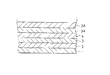
RRIFF nF~s~RlpTl~3N ~F THF nRAWlN~.~
s Fig. 1 is a schematic view illustrating a structure ~f a
ceramic substrate in accordance with the invention.
nF~S~RlPTlnN ~F ~HF PRFFFRRFn FMR~IMFNT~
Preferred embodiments in accordance with the present
0 invention wi~l be explained hereinbelow with reference to a drawing.
EM~ODIMENT 1
A multl-layer substrate in accordance with a first
embodirnent is formed by means of a green sheet manufacturing
process. First, alurninum oxide ~alumina) powder is screened to obtain
particles having the size ran~ing fr~m 0.8 to 1.2 micrometers, and
similarly borosilicate glass powdcr is screened to obtain p~rticles
having the size rangin~ from 1 to 3 microrneters. Then, the particles
of aluminum oxide and borosilicate ~lass are mixed with each other so
that each of them occupy 50% by weight of the mixture. Then, the
mixture is further mixed with or~anic vehicle into a slurry phase.
Then, a green sheet 1 having a desired thickness is manufactured by a
slip-casting process, and subsequently through holes are formed, the
holes are filled with a paste, and a pattern of electrical conductor 2 is
2s printed on the ~reen sheet 1.
A paste with which the electrical conductor 2 pattern is
printed on the green sheet 1 is composed of Ag, AgPd or AgPt. A
specific resistance of a sintered conductor is required to be less than
~''A 7
2137388
1 o ~n cm, because if the specific resistance is larger than 10
,uQ ~ cm, there can be obtained no merit of alumina multi-layer
substrate including electrical conductors ~ osed of tungsten (W)
having a specific resistance in the range of approximatelylO to ~0
5 ~Q ~ cm. Accordingly, when an electrical conductor is to be composed
of AgPd or AgPt, the electrical conductor is required to include Pd or
Pt in the range of 5% or less by weight on the basis of the weight of
the electrical conductor~
After a pattern of the electrical conductor 2 has been formed,
o a paste of AgPd or AgPt is screen-printed on the electrical conductor 2
to thereby form a barrier layer 3. As mentioned earlier, the weight
percent of Ag in the barrier layer 3 has to be lower than that of the
electrical conductor 2. The lower the weight percent of Ag in the
barrier layer is7 the more effectively a diffusion of Ag- atoms is
15 prevented. However, if the content of Pd or Pt is raised, the cost
would be increased and also a resistance of the barrier layer 3 could
not be disregarded. Hence, the weight percent of A~ in the barrier
layer 3 is preferably in the range of 60 to 90%.
Then, a resistive paste is applied on the barrier layer 3 to
20 thereby fornl a resistive layer 4. Further, on the resistive layer 4 is
dep~sited a second barrier layer 3A, and a second electrical conductor
pattern 2A is formed on the second barrier layer 3A so that a barrier
layer is located between a resistive layer and an electrical conductor.
After repeating this step tO thereby a laminated structure, the
25 resultant structure is sintered at the temperature in the range of 800
to 900 degrees centigrade.
The thus manufactured multi-layer substrate is cut by 100
mm x 100mm. Then, seven internal resistors are formed in the 100
2137388
mm x 100mm su~slrate. An experiment, in which actual resistance
values of the seven internal resistors were measured, was conducted
to confirm the advantageous effects of the invention. The results are
shown in Table 1 in which T-1 to T-7 indicates each of the seven
5 resistors~ Each of the resistors has a square cross-section of 50mm x
SOmm so that all of the resistors have 50 n of a resistance. It should
be noted that a resistor which can be practically used is one having 50
i Z0 Q of a resistance.
2137388
T A B L E
UNIT: RESISTOR Q
CONDUCTOR wt%
BARRIER LAYER wt%
NO. CONDUCTOR BARRIER RESISTOR
LAYER T-l T-2 T-3 T-4 T-5 T-6 T-7
1 Ag(100) NOTHING RuO2 115 61 35 42 190 21 84
2 Ag(100) AgPd(90/10) RuO2 62 53 48 38 66 38 55
3 Ag(100) AgPd(80/20) Ru02 68 49 32 32 60 44 61
4 Ag(100) AgPd(60/40) Ru02' 53 49 46 51 51 48 52
Ag(100) NOTHING IrO2 183 99 84 65 173 41 21
6 Ag(100) AgPd(90/10) IrO2 61 70 56 45 65 49 48
7 Ag(100) NOTHING RhO2 143 74 94 35 91 38 94
8 Ag(100) AgPd(90/10) RhO2 65 70 51 48 62 49 46
9 AgPd(95/5) NOTHING RuO2 162 94 95 21 32 26 105
AgPd(95/5) AgPd(92/8) Ru02 142 105 33 101 83 51 22
11 AgPd(95/5) AgPt(90/10) RuO2 62 53 48 50 49 36 52
12 AgPd(95/5) AgPt(70/30) RuO2 50 48 49 50 53 48 47
2137388
The followings can be confirmed from Table 1.
1. If the barrier layer would be formed, a dispersion of a
.resistance is larger than :~ 20 n.
2.. If the content of Ag in the electrical conductor is larger than
5 the content of Ag in the barrier layer, a dispersion of a resistance is
lars3er than ~ 20 n.
EMBODIMENT 2
In a second em~odiment, when a paste of ~gPd or ~gPt is
10 manufactu~ed, organic silicate is additionally mixed with particles of
AgPd or AgPt and organic vehicle, and then the mixture is mixed by
means of three rolls. The ~rganic silicate is oxidized while the
su~S~rate is being sintered, and thereby forms a ultra-thin SiO2 oxide
laye~ a~ound the particles of AgPd ~r AgPt. Then, the same experiment
15 as the first embodiment was conducted. The results are shown in
Table 2.
11
2137388
T A B L E 2
UNIT: RESISTOR Q
CONDUCTOR wt%
BARRIER LAYER wtX
NO. CONDUCTOR BARRIER RESISTOR
LAYER T-l T-2 T-3 T-4 T-5 T-6 T-7
1 Ag(100) AgPd(90/10) RuO2 51 49 47 46 53 48 55
2 Ag(100) AgPd(80/20) Ru02 46 50 51 49 50 48 52
3 Ag(100) AgPd(60/40) RuO2 51 49 47 52 50 49 51
4 Ag(100) AgPd(90/10) IrO2 52 50 46 51 48 49 50
Ag(100) AgPd(90/10) RhO2 46 51 51 49 47 49 53
6 AgPd(95/5) AgPt(90/10) RuO2 49 53 47 50 51 46 52
7 AgPd(95/5) AgPt(70/30) RuO2 46 49 47 54 51 48 49
2137388
It was confirrned from Table 2 that a diffusion of Ag atoms is
further prevented than the first embodiment, and that a dispersion of a
resistance of the seven resistors can be decreased less than ~ 10 Q by
coating AgPd or AgPt particles present in the barrier layer with sio2.
While the present invention has been described in connection
with certain preferred embodiments, it is to be understood that ~he
subject matter encompassed by way of the present invention is not to
be limited to those specific embodiments. On the contrary, it is
intended for the subject matter of the invention to include all
alternatives, modifications and equivalents as can be included within
the spirit and scope of the following claims.