Language selection

Search

Patent 2137413 Summary

Third-party information liability

Some of the information on this Web page has been provided by external sources. The Government of Canada is not responsible for the accuracy, reliability or currency of the information supplied by external sources. Users wishing to rely upon this information should consult directly with the source of the information. Content provided by external sources is not subject to official languages, privacy and accessibility requirements.

Claims and Abstract availability

Any discrepancies in the text and image of the Claims and Abstract are due to differing posting times. Text of the Claims and Abstract are posted:

  • At the time the application is open to public inspection;
  • At the time of issue of the patent (grant).
(12) Patent: (11) CA 2137413
(54) English Title: METHOD OF MANUFACTURING A GROUNDING CONNECTOR AND IMPROVED GROUNDING CONNECTOR
(54) French Title: METHODE POUR LA FABRICATION D'UN CONNECTEUR DE MISE A LA TERRE ET CONNECTEUR DE MISE A LA TERRE AMELIOREE
Status: Expired and beyond the Period of Reversal
Bibliographic Data
(51) International Patent Classification (IPC):
  • H01R 04/66 (2006.01)
  • H01R 04/28 (2006.01)
  • H01R 04/30 (2006.01)
  • H01R 04/50 (2006.01)
  • H01R 04/52 (2006.01)
  • H01R 43/00 (2006.01)
  • H02B 01/16 (2006.01)
(72) Inventors :
  • ROOSDORP, JOANNES WILLEM MARIA (Brazil)
  • YAMADA, WILSON MITSUDI (Brazil)
  • SORIANO, ALEXANDRE MARTINEZ (Brazil)
(73) Owners :
  • THE WHITAKER CORPORATION
(71) Applicants :
  • THE WHITAKER CORPORATION (United States of America)
(74) Agent: SMART & BIGGAR LP
(74) Associate agent:
(45) Issued: 2000-10-17
(22) Filed Date: 1994-12-06
(41) Open to Public Inspection: 1995-07-18
Examination requested: 1996-11-22
Availability of licence: N/A
Dedicated to the Public: N/A
(25) Language of filing: English

Patent Cooperation Treaty (PCT): No

(30) Application Priority Data:
Application No. Country/Territory Date
PI 9400114-6 (Brazil) 1994-01-17

Abstracts

English Abstract


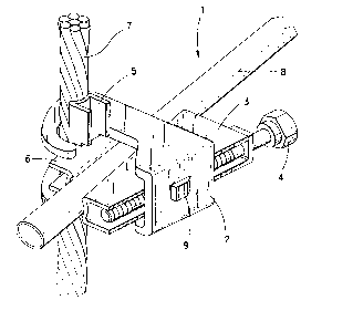
A method of manufacturing grounding connectors
(1) based on a stamping process on progressive
tooling which can produce a grounding connector (1)
which is lighter, of a reduced size, and is of low
manufacturing cost. The wedge type grounding
connector (1) comprises a hollow body (2), a wedge
(3), a shear-head bolt (4), two nests (5, 6) for
grounding cables (7) and rods (8), and a solid
fixture block (9). With the exception of the
fixture block (9), all components of the grounding
connector (1) are light, and of a reduced size since
these components of the grounding connector (1) are
manufactured by a stamping process.


Claims

Note: Claims are shown in the official language in which they were submitted.


6
CLAIMS:
1. In a method of manufacturing grounding connectors
comprising a wedge member; at least one nest member; and a body
having a generally hollow inner portion and a window for
receiving a fixture block; the improvement comprising:
sequentially forming said wedge member, said nest
member; and said body member from the same metal strip using a
metal stamping process on a progressive tooling machine.
2. An electrical connector for use with a grounding
circuit, comprising:
a wedge member;
at least one nest member; and a
body member having a generally hollow inner portion
and a window for receiving a fixture block.
3. The electrical connector of claim 1, wherein the
fixture block is disposed in said window for engaging a
tightening bolt.
4. The electrical connector of claim 3, wherein a portion
of the fixture block is disposed in said wedge member.
5. The electrical connector of claim 4, wherein the at
least one nest member is arranged to receive a conductor
thereagainst.
6. The electrical connector of any of claims 2 to 4, in
which there are two nest members, one of which is arranged to

7
receive a conductor thereagainst and the other of which is
arranged to receive a grounding rod thereagainst.

Description

Note: Descriptions are shown in the official language in which they were submitted.


213413
"METHOD OF MANUFACTURING A GROUNDING
CONNECTOR AND IMPROVED GROUNDING CONNECTOR"
The present application relates to a method of
manufacturing grounding connectors, and to an
improved grounding connector manufactured according
to the method. More specifically, the present
invention relates to a process of manufacturing
grounding connectors which produces a grounding
connector that is lighter, is of a reduced size, and
is of a low manufacturing cost, since the components
of the grounding connector are manufactured by a
stamping process.
The sophistication and sensitivity of
electronic systems and equipment used in telephone
companies and in industry, in general, has created a
demand for the development of consistent and
reliable grounding systems to protect the circuits
from electrical surges due to power variations and
other causes. Grounding systems provide a path for
the transfer of electrical energy, either for
intentional or accidental reasons, to the earth
thereby protecting electrical equipment.
Therefore, grounding connectors of the wedge-
type were developed. The grounding connectors are
reliable and require no special installation
equipment other than a common socket, ratchet, or
impact wrench. The simplicity of the installation
eliminates the requirement of special skills, which
in turn minimizes application time. Additionally,
the grounding connectors of the prior art present
the advantage of being applied in virtually all
weather conditions and situations.
However, the above-described grounding
15843 CA

w 2 2137413
Connectors present the disadvantage of being heavy and non-
compact since the grounding connectors are comprised of a
strong, solid body of copper alloy which is manufactured by a
die-casting process.
Consequently, it is desirable to develop a method of
manufacturing grounding connectors, which reduces raw material
usage and thus reduces the manufacturing cost of the grounding
connectors, thereby permitting the manufacturing of improved
grounding connectors, but which are more practical and of a
lighter weight.
The present invention discloses a stamping
manufacturing process for wedge-type grounding connectors, and
further discloses an improved grounding connector.
The manufacturing process proposed for the
manufacturing of grounding connectors of the present invention
is based on a stamping process utilizing progressive tooling,
i.e., it is based on the entering of raw material, for example a
metallic strip, in the tooling wherein all conformation steps of
the grounding connectors are performed in a sequential way,
inside the progressive tooling. At the end of the process, the
grounding connectors come out from the tool entirely finished
and ready to be used.
In summary, the method provides in a method of
manufacturing grounding connectors comprising a wedge member; at
least one nest member; and a body having a generally hollow
inner portion and a window for receiving a fixture block; the
improvement comprising: sequentially forming said wedge member,
said nest member; and said body member from the same metal strip
using a metal stamping process on a progressive tooling machine.
Thus, there is obtained a grounding connector
employing less raw material and in a quicker way than the
manufacturing process for manufacturing grounding connectors
employed in the prior art which uses a die-casting process.
A;

32137413
Further, the present invention provides an electrical
connector for use with a grounding circuit, comprising: a wedge
member; at least one nest member; and a body member having a
generally hollow inner portion and a window for receiving a
fixture block.
The components are lighter, of a reduced size and of a
low manufacturing cost since the components of the grounding
connector are manufactured by the stamping process described
above.
Additional features of the invention will become
apparent and a fuller understanding will be obtained by reading
the following detailed description made in connection with the
accompanying drawings, wherein:
Figure 1 is an exploded view showing the components of
a grounding connector of the present invention;
Figures 2A and 2B are sectional views showing the
assembled grounding connector of Figure 1;
Figure 3 is a schematic view showing the assembled
grounding connector of the present invention.
The improved grounding connector 1 of the present
invention, manufactured by a progressive tooling stamping
process, is basically comprised of a hollow body 2, a wedge 3, a
shear-head bolt 4, two nests 5, 6 for grounding cables 7 and
rods 8 and a fixture block 9.
The hollow body 2 of the grounding connector 1 has a
general double "J" shape, the two portions in the "J" shape
being joined together by one of the ends of the body 2 where a
window 10 is found, the window 10 being of a rectangular shape
and is designed to receive the fixture block 9.
The wedge 3 has a general trapezoidal shape and
la

213~~13
- 4 -
is also hollow and has a through hole 11 to receive
the shear-head bolt 4. The shear-head bolt 4 used
on the present invention is of the same type used on
the existent grounding connectors. Nests 5, 6 have
general rectangular "U shaped" cutouts 12 in side
walls 14, which are designed to accommodate specific
wires or a rod size combination.
The fixture block 9 of the present invention is
of such a size as to be fit into the rectangular
window 10 of the hollow body 2, and, further, a
through hole 13 is formed therein to receive the
shear-head bolt 4. The function of fixture block 9
is to support the shear-head bolt 4 and to move
wedge 3 towards the grounding rod 8 so that it can
be pressed against the body 2, nests 5,6 and the
cable 7. The wedge 3 of the grounding connector 1
is pre-assembled on the body 2, by the bolt fixture
block 9 and the shear-head bolt 4 before starting
the conductor assembly.
2o For application of conductors in the grounding
connector 1, it is necessary to manually back out
the shear-head bolt 4 until placing wedge 3 against
the rod 8; next, cable 7 is pulled into the J-
portion of the body 2 of the grounding connector 1
as shown in Figure 3. Then nests 5, 6 are placed
between the two conductors, using the suitable nest
sides which are designed to accommodate cable 7 of
grounding rod 8. Each nest is designed to
accommodate a specific wire or rod size combination.
Further, the wedge 3 is pushed into connector 1
and the shear-head bolt is manually pre-tightened.
Then, the fixture block 9 of the shear-head bolt 4
will be fixed in the hollow body 2 by the action of
15843 CA

213'~~13
- 5 -
opposite reaction forces on the side boarders of the
fixture block 9 when the shear-head bolt 4 is
tightened, thereby pushing the wedge into the hollow
body 2 as shown in figures 2A and 2B.
Finally, using a socket wrench or its
equivalent, shear-head bolt 4 is tightened until a
specific torque is reached, thus indicating the
conclusion of the connection by means of shearing
off the bolt head. The taper of wedge 3 forces the
body to spring open thereby resulting in a spring
action of the body 2 on the grounding rod 8 and
cable 7.
Although the invention has been shown and
described with respect to a best mode embodiment
thereof, it should be understood by those skilled in
the art that the foregoing and various other
changes, omissions, and additions in the form and
detail thereof may be made therein without departing
from the spirit and scope of the invention as
claimed in the appended claims.
15843 CA

Representative Drawing
A single figure which represents the drawing illustrating the invention.
Administrative Status

2024-08-01:As part of the Next Generation Patents (NGP) transition, the Canadian Patents Database (CPD) now contains a more detailed Event History, which replicates the Event Log of our new back-office solution.

Please note that "Inactive:" events refers to events no longer in use in our new back-office solution.

For a clearer understanding of the status of the application/patent presented on this page, the site Disclaimer , as well as the definitions for Patent , Event History , Maintenance Fee  and Payment History  should be consulted.

Event History

Description Date
Inactive: Inventor deleted 2021-11-23
Time Limit for Reversal Expired 2011-12-06
Letter Sent 2010-12-06
Inactive: IPC from MCD 2006-03-11
Grant by Issuance 2000-10-17
Inactive: Cover page published 2000-10-16
Inactive: Final fee received 2000-07-17
Pre-grant 2000-07-17
Letter Sent 2000-01-24
Notice of Allowance is Issued 2000-01-24
Inactive: Application prosecuted on TS as of Log entry date 2000-01-20
Inactive: Status info is complete as of Log entry date 2000-01-20
Inactive: Approved for allowance (AFA) 2000-01-12
Inactive: Delete abandonment 1999-09-17
Inactive: Adhoc Request Documented 1999-09-17
Inactive: Abandoned - No reply to s.30(2) Rules requisition 1999-07-21
Inactive: S.30(2) Rules - Examiner requisition 1999-01-21
Request for Examination Requirements Determined Compliant 1996-11-22
All Requirements for Examination Determined Compliant 1996-11-22
Application Published (Open to Public Inspection) 1995-07-18

Abandonment History

There is no abandonment history.

Maintenance Fee

The last payment was received on 2000-09-22

Note : If the full payment has not been received on or before the date indicated, a further fee may be required which may be one of the following

  • the reinstatement fee;
  • the late payment fee; or
  • additional fee to reverse deemed expiry.

Patent fees are adjusted on the 1st of January every year. The amounts above are the current amounts if received by December 31 of the current year.
Please refer to the CIPO Patent Fees web page to see all current fee amounts.

Fee History

Fee Type Anniversary Year Due Date Paid Date
MF (application, 3rd anniv.) - standard 03 1997-12-08 1997-09-19
MF (application, 4th anniv.) - standard 04 1998-12-07 1998-09-24
MF (application, 5th anniv.) - standard 05 1999-12-06 1999-09-21
Final fee - standard 2000-07-17
MF (application, 6th anniv.) - standard 06 2000-12-06 2000-09-22
MF (patent, 7th anniv.) - standard 2001-12-06 2001-11-02
MF (patent, 8th anniv.) - standard 2002-12-06 2002-11-04
MF (patent, 9th anniv.) - standard 2003-12-08 2003-11-05
MF (patent, 10th anniv.) - standard 2004-12-06 2004-11-04
MF (patent, 11th anniv.) - standard 2005-12-06 2005-11-22
MF (patent, 12th anniv.) - standard 2006-12-06 2006-11-17
MF (patent, 13th anniv.) - standard 2007-12-06 2007-11-20
MF (patent, 14th anniv.) - standard 2008-12-08 2008-11-17
MF (patent, 15th anniv.) - standard 2009-12-07 2009-11-18
Owners on Record

Note: Records showing the ownership history in alphabetical order.

Current Owners on Record
THE WHITAKER CORPORATION
Past Owners on Record
ALEXANDRE MARTINEZ SORIANO
JOANNES WILLEM MARIA ROOSDORP
WILSON MITSUDI YAMADA
Past Owners that do not appear in the "Owners on Record" listing will appear in other documentation within the application.
Documents

To view selected files, please enter reCAPTCHA code :


To view images, click a link in the Document Description column. To download the documents, select one or more checkboxes in the first column and then click the "Download Selected in PDF format (Zip Archive)" or the "Download Selected as Single PDF" button.

List of published and non-published patent-specific documents on the CPD .

If you have any difficulty accessing content, you can call the Client Service Centre at 1-866-997-1936 or send them an e-mail at CIPO Client Service Centre.


Document
Description 
Date
(yyyy-mm-dd) 
Number of pages   Size of Image (KB) 
Drawings 1995-07-17 3 75
Representative drawing 2000-09-19 1 14
Description 1995-07-17 5 198
Claims 1995-07-17 1 30
Abstract 1995-07-17 1 19
Description 2000-01-11 5 211
Claims 2000-01-11 2 38
Representative drawing 1999-12-01 1 24
Commissioner's Notice - Application Found Allowable 2000-01-23 1 166
Maintenance Fee Notice 2011-01-16 1 171
Correspondence 2000-07-16 1 39
Fees 1996-11-25 1 76
Fees 1996-08-27 1 62
Prosecution correspondence 1994-12-05 4 149
Prosecution correspondence 1996-11-21 1 44
Examiner Requisition 1999-01-20 2 56
Courtesy - Office Letter 1997-01-06 1 61
Prosecution correspondence 1999-07-20 2 66