Note: Descriptions are shown in the official language in which they were submitted.
- ~ 137568
1--
The present invention is directed to a semiconductor
electromagnetic detector and a method of detecting
electromagnetic radiation, and is directed particularly
to a semiconductor infrared detector having doped quantum
wells separated by finite-period superlattices. -
Detection of electromagnetic radiation in the mediumwavelength infrared (MWIR) band (wavelengths from 3-5
micrometers (~m)) can be accomplished with several
materials, e.g., indium antimonide InSb). On the other
hand, there is only one common detector for the long
wavelength infrared (LWIR) band (wavelengths from 8-12
~m): the narrow-band-gap semiconductor mercury cadmium
telluride (HgCdTe).
Many problems with respect to the uniformity of
optical and electrical properties and mechanical
stability are associated with HgCdTe. As a result,
routine fabrication of large HgCdTe detector arrays is
not possible. In addition, detectors that are sensitive
to more than one band of wavelengths at the same time
(sometimes called "two-color" detectors) are not readily
available.
Recently, semiconductor structures that have
dimensions small enough to make quantum mechanical
effects important have been described in the literature,
e.g., M. Sundaram et al., "New Quantum Structures",
Science vol. 254, pp. 1326-1335 (Nov. 29, 1991).
Conventional quantum well infrared photodetectors (QWIPs)
respond to thermal radiation with an increase in
electrical conductivity that results from internal
photoemission of charged carriers from energy states
confined in
VLS:jj
~;
~i3756'8
wo 94/00884 Pcr/uss3/o6l93 _-
~' 2
yu~lulll wells. Typical m~t~ri~lc used for cc~ cr,l;nn~l QWIPs are m-v C(;,ll~und
semiconductors such as ~ m arsenide and ~lllminnm g~ lm ~rsmi~P A typical
QWIP is a stack of layers in which the layers' m~t~n~lc and widths are carefully~l~P~t~ to achieve a desired distnbution of energy states for the device's elecLIul~s.
See, e.g., B. Levine et al., "New 10 ~Lm Infrared Det~ctor Using In~ulJb~
Absorption in R~snn~nt Tnnnrling GaAlAs Su~ l~ll;rrs", Appl. Phys. Le~t. vol. 50,
pp. 1092-1094 (Apr. 20, 1987).
An e~ pl& of the energy states in a convenhnn~l, unhi~d QWIP
such as that decrnbed in the Levine et al. paper is ill~-st~t~ in Fig. 1(a). Such a
10 convention~l QWIP is de~ be~ in. (~ene~l aspects of s~ , ;rPs, which typically
are structures of thin ~ g layers of two m~tPri~lc having different clccl,onic
pro~Lies, are described in G. Dohler, "Solid-S~ate Superl~ic~s", Sci~Pnt;fir
~mPrir~n vol. 249, pp. 144-151 (Nov. 1983). It will be l~ndprstood that
superl~ttir~s as well as the other structures d~pc~rihed in this applir~tinn~ can be
15 fabricated by a wide ~~ariety of m~thods~ e.g., vapor depocitinn m~.thn-ic such as
molecular-bearn epita~y and clech~ h~ ..ir~l depQcitinn m~tho~1c See, e.g., J.
Switzer et al., ~Elec~ d r~mic SU~ l;~ll;r~s", .~ci~nrr vol. 247, pp. 444-
445 (Jan. 26, 1990).
Three of the QWIP's quanlu", wells QW are seen in Fig. l(a), and the
20 wells have widths and energy depths that are chosen to provide two confined states,
the ground state and the e~cited state. The energy sep~dL.on between the ground
state and the e~cited state is set equal to the energy of the photon to be det~t~d by
the QW~, and generally increases as the width of the layers co~ ~n~ing to the
quantum wells QW decreases. The well layers are doped with electron donor
~5 impurities, e.g., silicon, thereby partially filling the lowest energy state with electrons
(as intlir~ted in the figure by the dashed lines). Barriers having thi~ sc~5 of
typically one hundred Angstroms (100 A) sep~r~t~ the quantum wells QW. Ln a
QWIP concicting of a stack of GaAs wells and Al"Gal ,~As barriers, the depth of the
wells can be varied over a ~ange of about 500 milli-electron-volts (meV). As noted in
~ 94/00884 ~13 7 5 6 8 pcr/us93/o6193
-- 3 --
the above-cited Sun~ram et al. paper, the we~depth is ylup~luonal to the dir~,clce
between the h~n~g~rs of the barrier and well layers, and varies almost linearly for
o.o < s < 0.45.
When a bias is applied to the QWIP as ~ ctrat~d in Fig. l(b), the
5 shape of the distribution of energy states ch~nges. Ele~trons can jump into the
escited states upon absorption of F~h~nc having the proper energy, and can tunnel
through the barriers se~lAI;ng the wells; the e electrons are co11~t~ as a current.
Conven*on~1 QWIPs operate at biases coll~ayonding to int~ l electric fields of
1~30 kV/cm, which are l~ui~d for effi~ nt extraction of the yhologe~P ,~tyl
10 carriers before recom~ ion. Due to the cl~L,o~s' tlmn~1ing from t~he ground state
through the thin ~ rs, howeva, the current that flows in the ~hs~nre of photons
(the "dark currentn) is ~In~ ptably large in the conventional QWIP.
Another type of QWIP is described in B. Levine et al., "High-
Detectivity D- = l.Ox10'~ cm ~Hz/W GaAs/AlGaAs Multi~luar"u,1l Well A = 8.3 ~Lm
Infrared De~c~ur~, Appl. Phys. Lett. vol. 53, pp. 29~298 (July 25, 1988). An
~s~mplt' of the energy states in such an l-nhi~d QWIP is ill~ ed in Fig. 2(a). In
this QWIP, the vidths of the ~lu~lul1l wells QW are chosen so that only the ground
state is bound in each well and the e~ccited state is slightly above the barrier in the
continm3m In such a QWIP, the barriers between the quantum wells are fairly thick,
20 e.g., ~loAill~ately 500 A, thereby yielding lower dark current when a bias is applied
as illustrated in Fig. 2(b). The carriers can still be collected because photon
absorption raises the electrons into the C4r~ ulll where they can be swept to the
QWIP's contacts by the applied electric field before recombination occurs.
Although the QWIP i~ ctr~ted in Figs. 2(a)-2(b) has lower dark current
~5 than the QWIP illustrated in Figs. l(a)-l(b), it has only one bound state in each
quantum well. Also, the energies of the first (virtual) excited states must be close to
the tops of the barriers because the photon absorption strength (i.e., the probability of
photoexcited transitions between states) decreases rapidly as the excited states move
further above the barrier. For a given operating wavelength, these requirements can
wo 94/00884 2 3 7 5 6 X ~ pcr/uss3/o6193
be ~ticfipd by only one combination of well width and barrier height, e~ h~l;n~ any
pOSci~ility of c~l~tin~ ~et~tor ~,Ç~i"ance by choosing different well widths and
.
barner colllyc)s.l.~nc
In ~A~itinn, the carriers' effective mass must be low if only one bound
5 state is allowed, thereby 1;...;L;j-~ such a QWIP to n-type dopants; this is
disadvantageous because p-type dopants can lead to devic~s having lower darLc
CUll~ i. Furthermore, the conventirJn~l QWIP's spectral bandwidth can be changedover only a very small range due to filnr~ nLal ylupe~Lies of optical e~rit~tinn of
confin~d carriers to coh~;n~J~ states. As a result of these plu~ies, ch~n~in~ the
10 s~t-~l bandwidth l~uil~ s pushing the e~cited states deeper into the COr~ uu~~~, but
as described above this ~l".",~;r~lly reduces the photon absorption strength, oruanlu~ effirirnry.
A QWIP theoretically analyzed in D. Coon et al., "Narrow Band
Infrared Det~tio~ in Multiquantum Well Structuresn, Appl. Phys. Lett. vol. 47,
pp. 289-291 (Aug. 1, 1985) has a single quanlul" well and a barrier concicting of a
supf l~ll;re Aspects of the Coon et al. paper are descrihed below, but it is il~l~l~nt
to note the paper admits that p~rtir~l ml~ltirle-quan~ulll-well de~lo.~ are beyond the
scope of the model it decrr1bes The ~u~ l~l;re barrier thichl~ocoes and co",pGsiLions
described in the Coon et al. paper (~u~ I~I;r~ periods, i.e., the ~ict~nrS~s hetween
~0 same-m~trri~l layers, r~nging from 114-94 A) provide a very narrow minib~nA Of
states (widths ranging from ~18 meV, l~ ely). In ~ ision, the paper describes
thi~knecc~5 and colllpos;l;o~nc that position the first excited state of the quantum well
in the lowest energy minib~nrl of the ~"~ l;r~ in order to obtain a narrow
bandwidth inf~ared det~tor that would have low dark current.
'5 The Coon et al. paper suggests that electron transport norrnal to the
plane of the quantum well should occur fairly easily. Nevertheiess as described
above, a bias is n~e~c~. y to transport the photoel~cited carriers for collection before
recombination occurs. Applying even the lowest typical bias to a detector such as
~ 94/00884 ~13 75 ~ 8 pcr/us93/o6193
that described in the Coon et al. paper would nender ert~rtinn of the photogenerated
carriers e AL~ cly riiffir?-1t and inPffiri~t
As de~ihed in E. ~ende7 et al., "Stark ~ oc~1i7~tinn in GaAs-GaAlAs
Su~r1~ttir~c under an F1~ic Field", Phys. Rev. Lett. vol. 60, pp. 2426-2429
aune 6, 1988) and R. I~avitt et al., "Stark Ladders in Strongly Coupled Super1~ttir~s
and Their Tntf. ~r!;nn~ with r~ d~d Quarllul~l Wells~, Phys. Rev. B vol. 41,
pp. 5174-5177 (Mar. lS, l990), for c~mp1e, minih~n~ states become strongly
lor~li7~d when the ~ drop across one S~ ;rc period is ct~ h1r to the
width of the minih~nd. The c~ntlitinn for 1n~1i7~ti-1~ of the ...;nih~nd states to a
10 single superl~ttir~ well is the ~Lcr,tial drop across one period should be equal to one-
half of the .llinih~nd width. Even tbe lowest bias typically n~c~ to l. .ntpo~L
carners out of a QWIP before recomhin~tinn would completely lor~li7~ the minih~n~
stat~s of the supe~1~ttir~s in the det~ r ~ecrrihed in the Coon et al. paper.
As a result of such loc~li7~tinn h~ns~l~ of phot~ cit~ c~ri~rs in the
15 det~tor decrrihe~ in the Coon et al. paper could occur only by tlmnplin~ ~elw~n tbe
localized minib~n~ and qua~lLulll well states. It will be ~ c~d that a tl~nnpling
transport process cannot be char~cte-i7~d as easy. Moreover, although the paper
suggests that l~ ..A.~hly high ~ effiriDnri~s might be achieved, in fact a
detector such as that dec~ihed in tbe paper would 1 ave a very low quantum effiripncy
20 because the probability of tbe carriers' tl~ lough the d~Pt~tor by t~mln~1ing is
cignifir~nsly less than tbe probability of tbeir recomhin~tinn
In ~ition, the Coon et al. paper describes a theoretical tre~tmPnt that
is valid only for miniband widths that are much smaller than the depths of the
superl~ r,e potential wells. Thus, much of the latter portion of the paper and even its
25 title are directed to considerations arising out of the narrowband limi~tion. Such a
narrow minib~nd would result in a d~PtP~tor having an advantageously low dark
current, but would intro~uce other problems. The minih~n~s described in the paper
are so narrow that, as the paper acknowledges, it would be a rh~11Pnge even to
position the quantum wells' excited states in lcsonance with the minih~nds.
2137568
Wo 94/00884 pcr/us93/o6193
The paper's applc,~ e snlnti~nc of Schroe~lingP~'s equation are
s--it~h1~P for ~ having minib~n~ic that are narrow to reduce dark current, but do
not permit ~r~ll~tP ~ e pr~ic inn, i.e., S~l~ ctinn of prçdetPnninP~
plope,hes, of biased MBT ~ lu,~ having wide minih~ntlc In fact, the paper
in~r~11~t~1y sugg~ that the QW~s absorption ~ye~hunl would have the same width
as the minih~nd and that the absorption strength would be almost c~nC~nt ~ g~outthis width. Thus, it is not surprising that the paper is silent on selectively positioning
the e~cited states within the minih~n~c and the consequent adv~nt~ous effects on the
absorption :~CC1.1UIII.
SUMMARY
One object of Applicant's invention is to provide an improved
semiconductor device for ~etP~tin~ cleehu...~gn~Ptir~ es~i~11y infrared, r7~ tinn
It is also an obiect of Applicant's invention to provide a minih~nA
transpon quantum well ~et~t~r that is most sensitive to a plcde~,lllined wavelength
15 and that is sensitive to a yl~dety ;~cd spect~al bandwidth.
It is another object of Applicant's invention to provide a minih~n~
transport QWIP having a spect-~1 response that is nearly constant over a broad range
of wavelengths such as the ~tmosph~rir tr~ncmiccinn windows of 3-5 ~m and
8-12 fLm.
It is a further object of Applicant's invention to provide a minih~n~
transport QWIP that is sensitive to r~ tion in one or more than one wavelength
band.
It is another object of Applicant's invention to provide a miniband
transport quantum well detector having predeterrnined electro-optical IJropelLies, e.g.,
dark-current depen~enc~ on applied bia voltage and response and detectivity
dependence on incident wavelength. Such properties are deterrnined by the density,
~1 37S~8
-
- 7 -
location, and type of the detector's dopants and by the thickness and composition of the
detector's layers.
It is another object of Applicant's invention to provide a minib~n~l transport
5 quantum well detector in which the wells' excited states are selectively positioned within
the miniband to i~ rove the detector's spectral response characteristics.
These and other objects are met by a minih~n-l transport quantum well
detector colllplising a substrate, a multilayer structure disposed on the substrate, and first
and second contact layers disposed on the top and bottom surfaces of the multilayer
10 structure. The multilayer structure colllpli~es a plurality of layers of first quantum wells
and a plurality of layers of second quantum wells wherein the number of first ~
well layers in the detector is differelll from the number of second quantum well layers.
The quantum well layers are interleaved with a plurality of superlattice barrier layers.
Each superlattice barrier layer colllplises a plurality of thin first layers having a relatively
15 low b~n-le~p interleaved with a plurality of thin second layers having a relatively high
bandgap, and has a miniband of energy states having a center and width determined by
the thicknesses and compositions of the thin first and second layers.
The thicknesses and compositions of the quantum well layers and of the thin
first and second layers of the miniband transport quantum well detector are such that
2 o each quantum well has a ground state and an excited state and the energy of the excited
state is subst~ntially equal to energies of selected states within the minibands of the
adjacent superlattice barrier layers. In this way, an electrically colllilluous channel
through the multilayer structure is provided, and the detector's optical characteristics,
such as the peak-response wavelength and the spectral bandwidth, are determined by an
25 interaction of the energy states of the quantum well layers and the minibands of the
superlattice barrier layers.
In accordance with one aspect of Applicant's invention, the energies of the
quantum well layers' excited states may be subst~ntially equal to the energies of a
predetermined pattern of states in the minih~nds, thereby obtaining an MBT detector
30 having predetermined optical characteristics.
in: j j
,;
Wo 94/00884 21~75 6 8 pcr/us93/o619~
-- 8 --
The objects of Applicant's inverrtion are also met by a two-color
minih~n~i transport ~U&l~UIll well de-t~tQr comprising a svbst~t~, a first multilayer
~uuc~ i~os~ on the s,-l,s~ , first and second contact layers Ai~ros~d on the topand bottom s~rf~r~s of the first multilayer structure, a second multilayer ~ c~un,
disposed on the first contact layer, and a thIrd contact layer ~ os~ on the second
multilaya structure distal from the first multilayer sLIuaul~. The fir t multilayer
structure compricPs a plurality of 4uanlull, well layers interleaved with a plurality of
su~,l~l;ce barrier layer, the ~ayers having thi~np-c~s and Co~ ?oc;l;9~c such that
the de~P~tor resprnds to a first wavelength band. The second multilayer structure
comrricPs a plu~lity of quanlul~ well layers intPrl~ved with a plurality of
s~ l;ce barrier layers, the layers having thirlrnPs~s and compo-citinnc such that
the detector recpon~c to a second wavelength band.
An MBT dt~ dl in acujldance with Applicant's invention comrricps a
plu~ality of quantum wells that e~ch have two bound energy states so that a widerange of m~tPri~1~ and carrier types may be used to obtain a pre~det~ P~
peak-response wave1~ng~h. In one e~hc~ p~t the MBT d~t~o~ inrllJAes
7~-A-wide GaAs yu~ulll well layers and GaAs/Al03GaO7As su~ l~ll;re barrier
layers to obtain a peak-recponc~ wavelength of about lO ~Lm. In another embodiment,
the MBT dete~t~r could include 87-A-wide GaAs quarllu", well layers and
GaAs/Al04GaO6As supPr1~ttir~ barrier layers to obtain subst~nti~11y the same
peak-response wave1en~th. In yet another ernho~imPnt, the MBT detP~tor inrllldes4~A-wide InO l5GaO t5As quanlu,ll well layers and Al0 3GaO 7As/Al0 4GaO 6As ~u~. l~n ice
barrier layers to obtain a peak-response wavelength of about S ~m.
Applicant's invention ~ iitioll~1ly encompasses a ~r ethod for detecting
'5 electrom~gnetic radiation with a semico~uctor device. The method includes the step
of providing a plurality of 4~lulll well layers having compositions and thir~npsces
such that predetermined excited state energies are obtaine~. The method further
includes the step of providing a plurality of superlattice barner layers interleaved with
the quantum well layers. The superlattice barrier layers have wide minib~nrlc that are
~. J 94t00884 213 7 5 B ~ pcr/us93/o6193
strongly and sele~Li~,ely coul.lrA to each other a-nd to the e~cited states of the 4u~nLulll
well layers. The method further inr~ es the steps of e~riting ~- . ;e. ~ in the yuantull,
well layers into the e~cited sta~ and minih~nrlc by photon absorption, applying an
electric field across the ~u~ .I~Il;r.e bar~ier layers and the ~luantulll well layers to
5 transport the e~cited c~- . ;e ~ uuy,ll the layers, and ccll~hng the ~n~portedcarriers as a phol~u~lcnt co"~onding to the mlmher of photons abs~,l~d.
BRIEF DESCRIPI~ON OF l~E DRAVV~GS
The invention and its objects and advantages will be understood from
the following det~ d~,i~lion and the ~c4...l-~.ving drawings, in which:
Figs. l(a) and l(b) illnctr~t~o the energy states of a conventinn~l QWIP
without bias and with bias"~i~ely;
Figs. 2(a) and 2(b) illtlCts~t~' the energy states of ~noth~or conv~n~ion~l
QWIP without bias and with bias"~;~ ely;
Fig. 3 illllclr~t~s part of the sernioQnductor structure of a minib~nd
15 transport ~ well det~l in accol~ cc with the present invention;
Fig. 4 i1 C,tT;3te,C a cross-section of a minih~nd tr~n~ort QWIP having
the se nir~nductor structure shown in Fig. 3;
Figs. S(a) and 5(b) illustrate the energy states of a minih~nrl transport.
q~ ulu well detector in ac~ordance with the present invention without bias and with
20 bias, res~li~ely;
Fig. 6 shows a measured l,hotoc~ nt response ~hUlll of a minih~n~
transport QWIP in which the energies of the excited states of the qu~lu,l- wells are
near the bottom of the minih~n~;
Fig. 7 shows the measured bias dep~ndenre of the detectivity of the
25 miniband transport QWIP of Fig. 6;
213756~
wo 94/00884 pcr/us93/o619~
- 10 -
Fig. 8(a) ill~ $ plr~ t~ sqn~ar~ wav~ful-rl;onc for a minih~n~
transport. quantum well dct~ t~r in which the energy of a ~luanlu--l well's e~ccited state
is near the bottom of the ,..ini~nrl-
Fig. 8(b) ill.~ t~s a c~lr~ ted absorption ~ h~ for a minih~n~
5 t~ansport QWIP ~ which the cne,~ies of the excited states are near the bottom of theminih~ nrl;
Fig. 9(a) illlicl.,.-~c ~lr~ t~d squared wavefun~tinnc for a minih~n~
transport 4uallLul~l well dc~tor in which the energy of a quanlu-ll well's e~ccited state
is near the center of the ,...nih~nd;
Fig. 9(b) ill~.cl.,.~f s a c~lr~ ted absorption ~ lll for a minih~n-i
transport QWIP in which the energies of the e~cited states are near the center of the
minih~n~
Fig. lO(a) ill~ s c~lr!llAt~ S lua~cd wavefunrtirJr1c for a minih~n~
transport quar.lulll well d~ ~ c~r in which the energy of a quantum well's excited state
15 is near the top of the ,..;.~ik~.ul
Fig. lO(b) ~ CllAt~s a Plrul~t~d ahsorption ~ ulll for a minibAn~
transport QW~P in which the energie of the e~cited states are near the top of the
minih~n~;
Figs. ll(a) and ll(h~) ill-)c~t~ measured photocurrent response spectra
20 of minih~nd trAncrort QW~s in aceor~nce with the present invention;
Fig. 12(a) ill~l5tr~t~5 the energy states of a broad-band minih~nd
transport qu~ul,l well det~tor in which the energies Of the e~cited states are
positioned in a pattern within the l--;.-;hqn~
Fig. 12~b) illmt~tes an absorption S~lllllll of the broad-band
25 minib~nd transport ~lu~llu", well det~tt r of Fig. 12(a);
Fig. 13 ill~lctr-At~c cAIrll~At~d relative absorption spect~ for miniband
transport QWIPs in accol~nce with the present invention;
213~68
~ 94/00884 pcr/us93/o6193
- 11 -
Figs. 14(a) and 14(b) illust~t~ measured absorption spectra for
minib~nd t~ansport QWIPs in which the energies of the e~ccited states are pocitinn~d
near the bottom of the minib~n-l and in a pattern vithin the minih~n~ ely;Fig. 15(a) illl-ct~t~s the energy states of a two-color minih~nd transport
5 4u~ ull, well detector in accordance with the present invention;
Fig. 15(b) shows a measured phot~cu~.~nt response ~peckulll for a
two-color minib~nd transport QWIP in acco~d~nce with the present invention; and
Fig. 16 illl,sl.AtP5 the energy states of a ~type minihAnd t~nc~ort
quantum well det~tor in ac~,dance with the present invention.
DETAILED DESCRImON
As described in more detail below, Applicant's semir~nductor
elecLIu~ gn~tiç det~tor comprises a plurality of doped ~uantum well layers se~.A~d
by finite-period ~ tl;re barrier layers. In accordance with Applicant's invention,
~he superl~t~ir~ barrier layers have ...;nih~nrlc of energy states that are el~trir~lly and
15 optically coupled to states of the ~uanlu.., wells. Thus, the su~~ ;re barrier layers
contribute subst~nti~lly to the optical ch~rt~ristics (e.g., the peak-l~s~
wavelength and the spect~al bandwidth) of the detector. Both the peak-response
wavelength and the spe~!ral bandwidth of the deteetor are determined by the
thi~knPccP5 and co,.-l os;tionc of the layers. The thirk~lesses and compositions can be
'O chosen from a wide range of possible values to obtain predetermined peak-response
wavelengths.
In accordance with Applicant's invention, the finite-period sUperl~sti~p
layers forrn actual baIIiers to carriers in the ground states of the quantum well layers.
Using superlattices as barriers permits more adjustability and control of detector
~5 characteristics than is possible with previous structures such as those described in the
aDove-cited papers by Levine et al. The number of periods in the finite-period
W O 94/00884 2 1 3 7 5 ~ 8 PC~r/US93/06193 _
- 12 -
~"~ t~tl;c~s is chosen s~1ffiriPnt1y large that d~k current due to tl-nnPling out of the
wells' ground state is s~bsl~..l;~lly el....;n~
Also, thc th~ cc~5 and cG~ Qs;l;onc of the thin layers of the
s-lpP 1~ttir~ barrier layers are Cf"~ t~;l such that the layers have minih~nAs that
5 strongly inLe ~I, or merge, wi~ the yuanlulll well layers' e~cited states. Mo~w~
the widths of the ~.~;nih~nAc of the s ~ l;re barrier layers are much larger than the
drop in ~t~ltial across a period of the ,~ l;re when the Aete~tor is biased. As
des~ rihe~A in the above-cited l~enA~7. et al. and Leavitt et al. papers, this ensures that
the minib~nAc do not break up into series of strongly 10~1i7~A states and the
lO minih~nAc remain strongly c~l1pW to each other. Thus, an el~tric~lly continl)ous
ch~nn~1 through the ~et~ctnr is provided despite the i,lte~l~Lion of the ;~u~ ll;r~s
by the ~luarllu~l~ well layers, which would otherwise impede the t~ansport of
phot~cited c~rriPr A carrier photo~cit~A lnto a well's e~cited state (or a
minih~n~ state) can be s~nCported easily under the inflll~onre of the applied bias
15 through the det~tor and be c~ ct~ at sllit~hl~ c~nt~rtC as phntoc~ . L
It will be a~ ch~d a A~ tor in acco-dance with Applicant's
invention is thus cignifir~nt1y difr~.~nt from previous dct~clo,~ such as that des~ihe~
in the above-cited Coon et al. paper. D~o ~ in accofd~ce with Applicant's
invention have ~..;nih~nd widths typically ranging from 50-120 meV and superl~ttir~
20 periods of 60 40 A, ~cs~Li~ely~ and thus loc~1i7~tinn effects are ci~nific~nt only for
very high internal electric fields (40-lS0 kV/cm, l~s~;~ ely). In contrast, the Coon
et al. paper diu~1os~s S~ tl;re layer thirl~n.occPs and compocitionc that yield a very
narrow (~18 meV) minih~n~ in order to obtain a narrow bandwidth infrared ~e~
Such super1~ttires would c~ rse into complet~1y lor~ii7~d states for the lO-30 kV/cm
~5 intrrT ~1 electric fields that are needed for e~traction of photogene~t~d carriers. It
will therefore be a~,c~_ia~d that the ~t~rtinn of phototo~rited ca~Tiers from the
Coon et al. det~tor would be extremely in~ffirirnt
In ~ tion~ the Coon et al. paper does not suggest that the det~tnr~s
response is partially det~ll.li,.ed by the relation between the wells' excited states'
2137568
94/00884 PC~r/US93/06193
- 13 -
ene-yies and the ~Ç~ ;iES of states in thc mini~ nrlc As~ics~ above, the paper's
thÇ~ret~ A~ is valid only for minih-Anri widths that are much smaller than the
depths of the ~ lAll;r~e pot~nl;~l wells, and leads tO aII absorption ~ hulll that has
the same width as the minih~An~ and is S~ SIA~II;A11Y co~ct-Ant throughout that width. It
5 will he a~l~ia~i that the ap~lu~;lllAl;nnc used in the paper should not he
e~ d to wide ...;n.hAntlc As dccr~ ed in more detail below, e~cact s~ tinnc(i.e., solutionc valid for all minih-And widths) to the Sc~ eA;nge~ equation for~c~lors in accor~ance with Applicant's invention show the e~cited state~s positinn
re}ative to the ~..;nih~nr~ has a ~l~fo~d effect on the abs~lyhon ~CChulll.
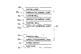
Fig. 3 ~ ctr-At~o~s part of the ~nicnnduetnr structure of a minihAn~
S~ncrort (~T) qu~u~Lull- well det~to- in a~coldance with Applicant's invention.
The MBT deL~lùl comp-i~s a plurality of ~luarlLulll well layers 10~-10~, int~rlç~ved
between a plurality of su~ lAtl;rr barrier layers 201-20n. The int.o-lr-Aved layers are
disposed on a s~bsl~At~ 30 and are a multilayer ~l~uclule d~not~ by the reference
15 n~m~rAl 40. A capping layer 60 and a buried contact 70 are provided on each end of
the multilayer structure 40.
Fig. 4 is a cross-section of a plurality of MBT d~ tl CI~J~ ~ that are
~nged as pixels in an arQy for ~k~ g LWIR r~i-Ati~n that is inrident lhlough
the sulJsLla~e. (Only three MBT ~ are shown in the figure, but it will be
20 a~l~,aled that the array may com~ i~ a larger nllmher of pL~els.) Each pi~el is
delin~ted and its buried contact 70 e~sed by suitably etching away the mAt~riAl
surrounding the pi~cds.
As ;11llCI.A~ in Fig. 4, each pi~el adv-Ant~e~ucty inrtudes an optical
rliffr~ctioll grating 80 that may be etched hto the capping layer 60 and that may have
~5 a metal contact depocit~d on its upper sl~fAee. It will be a~ ed that light
incid~nt through the subs~ate 30 is not ~et~t~ as it passes through the multilayer
structure 40. The gratings, which have riimrnciQnc and effiriencies a~r~liate for
the wavelengths to be det~t~, produce a diffr~cted colllponent of the inrident light
that is polarized perpen~ir!ll-Ar to the ~e~ ' layers and that is det~ted It will be
~ 3756~
-14-
understood that such a polarization is required by the
selection rules governing the absorption of infrared -
light in quantum wells, as described in, e.g., L. West et
al., "First Observation of an Extremely Large-Dipole
Infrared Transition within the Conduction Band of a GaAs
Quantum Well", Appl. Phys. Lett. vol. 46, pp. 1156-1158
June 15, 1985). Thus, the gratings facilitate
fabrication of two-dimensional arrays of MBT detectors.
The upper-surface metallization is advantageous because
it permits mass electrical connection to the detectors in
an array by a technique such as indium-bump bonding.
Instead of or in addition to the gratings 80, any of
the various known techniques for increasing the
proportion of the incident light that may be detected may
be used with Applicant's MBT detectors. For example, the
grating lines may be etched into the surface of the
substrate 30 if the imaging properties of the array are
not important. The photons diffracted through the
detectors may then be reflected by metallic capping
layers 60, and the reflected photons would have another
chance at absorption in the array pixels. Also, two-
dimensional gratings might be used, although such
gratings would have some effect on efficiency.
In accordance with one aspect of Applicant's
invention, each of the quantum wells formed in layers
10l-10n contains a ground state and an excited state. In
addition, each of the superlattice barrier layers 201-20n,
is comprised of a plurality of thin, lower-bandgap layers
(quantum wells) separated by thin, higher-bandgap layers
(barriers). As described above, the superlattice layers'
thicknesses and compositions are chosen so that the
energy states of the thin quantum wells merge to form a
wide (approximately 50-150 meV) miniband of energy states
that is in resonance with the excited states of the
quantum well layers 10l-10n.
VLS:jj
?1 37~6~
-14a-
As used in the current application, "resonance"
between a superlattice barrier's miniband and a quantum
well's excited state means that the energy of the well's
excited state is either slightly below the miniband's
lowest energy (viz., at the "bottom" of the miniband),
between the miniband's lowest and the highest energies,
or slightly above the miniband's highest energy (viz., at
the "top" of the miniband).
VLS:jj
.. .
2137568
' .-J 94/00884 ~- - Pcr/us93/06193
- 15 -
This re1~tionchi~ is also referred to below as on-e in which the excited state is
poci~innpA within the ..,.nih~nA hPC~llc~ the minih~nA, of a f~nite-penod ~ur ~l~lI-r~
barrier does not di~dp~ completely outside the barrier but c4~l;nllr~ into the
adjacent quantum wells. If the ~ua~lul~ well's excited state is po~itinred below the
5 bottom or above the top of the minih~nd, it is believed that such an e~ccited state's
energy should be, as a p~rtir~l matter, within 5-10 meV of the ...;n.h~r~A's top or
bottom in order to ..~in~ coupling between the excited state and the minib~nA. For
excited states further away from the minih~1~d~ the ~ would have to tunnel into
the minih~nd
An e-~".l~lr of the energy states of an unbiased MBT d~ lor in
accordance with Applicant's invention is illllct~tQ in Fig. 5(a), which shows the
excited states of the ~uarllulll wells QW-102, QW-103 falling ~el~.~n the top and
bottom of a minih~nA, 100 formed by the svpc~ ;ce barrier layers 20,-203 co~npric~
of thin barrier layers 110 and thin well layers 120. The qua~ , well layers 102, 103
are ~ bly doped so that the wells' ground states are par~ally filled with c~ rs
(si~nifi~l by the dotted lines in the wells QW-102, QW-103).
Fig. 5(b) illustrates the effect on the energy states of an electric field
applied to the structure: the minih~nA, 100 iS tilted. The ~rrjDrS in the ground states
of the quantum wells may thus be lifted into the wells' e~cited states or the minih~nA
states by the absorption of suitably energetic photonc (three are shown in the figure).
With the wells' excited states in .es;!n~nc~ with the superl~tic~ barriers' minih~nAs,
the minih~nAc remain strongly coupled to each other and the prob~hility of
photoinducwA transitions into minih~nd states is increased. In this way, the carriers
can move with relative ease under the influ~nce of the applied bias through the layers
10,-10D, 20,-20n for collection at the contact laya 70 as a photocu~l~nt.
The s~ r~ barrier layers 20,-20n are preferably of such a
thicknesc that the probability of carriers ~mn~linE directly from one quar,lUl.l well's
ground state into the states in the adjacent well, the minib~nd~ or the continuum is
suhstantially zero for the biases typically applied to the structure. In other words, the
Wo 94/00884 2 1 3 7 S 6 8 Pcr/US93/06193 __
-~ 16 -
tnnn~oling cc ~ oncl~t of the dark current is a~plu~ ely zero for Applicant's MBT
det~ctor, which is in shalp c~7nt~ct to the convenrinn~l QWIP behavior illy~lrAled in
Fig. 1(b).
Also, the heights of the thin barrier layers of the su~;.lzll;r~ barrier
layers 20,-20" are preferably such that the prob~hility of thermionic emiCcion of
carriers into states above the barriers (i.e., stadtes in the collLi,luulll) is suhst~nti~lly
zero for the ~BT det~ctor's o~.dling ~r ~ .,.I...e. MBT ~e~ol~ suitable for the
MWIR and LWIR bands would typically operate at about 77 K. Under these
c~nrlitinnc, the MBT d~l~clul's dark current results from thermionic emission of10 carriers into the ...inih~n~, and thc,cru~ ~n~C on the di~re.~nce in energy beL~een
the wells' ground states and the bottom of the minih~n-l
An MBT ~et~t~r in accordance with Applicant's invention hds been
made by mol~ul~r-beam epita~cy on a GaAs substrate. The MBT ~t~ctor int~ Ps
for~ GaAs yu~llulll well layers, each of which is 78 A thick and is doped with
silicon to a c~n~nt ation of 4~101' cm-3. The yuanlulll well layers are SC~IA~ by
su~ tl;c~ barrier layers in the ll~mc~ ~ in Fig. 3; each surP~l~ttire barrier
layer is comprised of nine thin GaAs wells, each a~pru~ t~ly 20 A thick, and tenthin Al03GaO~As ba~.ie,~, each ~ JIim~t~ly 40 A thick. The MBT det~tor had
l-~m-thick capping and buried contact layers made of heavily doped GaAs formed
20 above and below the active q~lanlulll well layers.
Such ~- poc;tinnc and th~ nloc~s of the quantum well and superl~tti~e
barrier layers yield an MBT det~rtQr having a minib~nd width of about ~0 meV, the
wells' e~cited states at the bottom of the minih~nd, and an energy difference between
the wells' ground and excited states of a~,o~ t~ly 118 meV. That energy
~5 difference corresponds to a peak-response wavelength of about 10.5 ~m. Calc~ tinnc
have shown that an MBT d~ or having 87-A-thick GaAs quantum well layers and
GaAs/Ab4GaO6As su~ e barrier layers would have subst~nti~lly the same optical
j,lupel~es. Thus, Applicant's invention provides for fabricating from a variety of
compositions and thic~ sces MBT detectors having similar ~lOpClLies.
~ 94/00884 21 3 7 5 6 8 pcr/us93/o6193
In an ~ ngem~nt similar to th~t illustrated in Fig. 4, a plurality of
such ~3T ~et~~ having various areas were then defLne~ on the subst~t~ by
ch~mir~1 etching. It will be a~i~iatxl that the upper limit on ~et~.lQ, si7e
(~et~lol~ as large as 500 ~m have b,een built) is usually de~~ ned by the acceptable
dark current, which is l,lupolLional to area, and to a lesser e~tent by defects produce~
dunng f~hri~tinn, The lowcr limit on A~ t ~; lor size (about l l m for MBT Ae~
which are typically about 2 4 ~m thick) is mainly determined by the etching and
litho~ phy l,locesses used. Instead of having ~rZ*n~.c disposed at the ca~ping layers
60 as shown in Fig. 4, ho~.~,ier, triangular gratings having a 4-~m-pitch were etched
into the substrate 30 so that light pol~ri7f~l perpen~lir~ r to the ~ anLulll well layers
was inci~lpnt on the pi%els. Also, ohmic metal cont~rtc were ~os;1ed on the capping
and (now partially e~posed) buried contact layers.
Figs. 6 and 7 i!h~st~t~ measured char~rtenctirs of one of the MBT
det~tors. Fig. 6, which shows the rel~tir~nchip between incid~nt wavelength and
MBT detector response (in ~ dly units of photocurrent), in~ir~5 a peak-responcP
wavelength of about 10.5 fLm and a long-wd~lelcngth cutoff (the half-peak point) of
about 11.1 ~um. Fig. 7, which shows the rel~tionchir between applied bias voltage
and detectivity at a det~t~r O~.dtilg ~".~ldture of 77 K, in~ic~tP5 the tested MBT
dete~tQr has a peak D- = lx101~ cm Hzln W-l.
It will be dp~l~ia~d that MBT ~et~tors and arrays can be made that
have other layer comrositinnc and th~ np~cps In particular, the energies of the
excited states and the minih~n~ states wl be chosen to obtain desired optical and
ele~t i~l char~ct~rictics, and the layer cGl~C;t;on~ and thi~Psses can be chosenfrom a wide range of possible m~tl~ri~lc and values. In general, MBT det~ols in
'5 accordance with Applicant's invention can be made from any m~t~ri~lc suitable for
mal~ng quantum wells, e.g., ~ ...;nu". gallium arsenide, pseudomorphically str~ined
indium gallium arsenide on gallillm arsenide substrates, and }attice-m~t~hed indium
-gallium arsenide on indium phosphide substrates. In addition, it will be appreciated
that such intersubband de~ectors on GaAs are currently most useful for wavelengths
~7-1~7~68
-18-
between about 3 ~m and about 19 ~m. Moreover, the
doping, which leads to the desired light absorption in
the quantum well layers, may be varied in concentration,
and possibly in position as well (i.e., the detectors may
be made with modulation doping of the superlattice
barrier layers).
It will be understood that the doping level
determines the strength of photon absorption, which is
directly proportional to the two-dimensional doping
density. On the other hand, as the doping level
increases, the fermi level of the ground state gets
closer to the bottom of the miniband, increasing
thermionic emission into the miniband and thus the dark
current. In general, it is believed that doping levels
in the range of about 1x1017 cm~3 to 2X1018 cm~3 are
suitable for the MBT detectors described in this
application. It will be appreciated that for MBT
detectors responsive to the MWIR band the doping levels
can be higher than they are for LWIR MBT detectors, viz.,
closer to 1013 cm~3, because the energy separation of the
ground state and the excited and miniband states is
greater. Also, lower operating temperatures would
typically permit higher doping levels without increased
dark current as described below.
Exact Airy function solutions of Schroedinger's
equation, including an applied field, are preferably used
to determine the energies and wavefunctions of carriers
in the quantum wells and the superlattice barriers of the
MBT detector. See, e.g., C. Weisbuch et al., Quantum
Semiconductor Structures, pp. 19-20, Academic Press
(1991) and M. Abramowitz et al., eds., Handbook of
Mathematical Functions, Applied Mathematics Series 55,
pp. 446-455, National Bureau of Standards, Washington,
D.C. (June 1964). In general, such solutions are sums of
Airy functions with boundary conditions imposed by the
detector structure that lead to discrete energy solutions
VLS:j;
~1 775~
-18a-
and specific carrier wavefunctions. (It will be
appreciated that the square of the wavefunction gives the
probability of finding the carrier at positions in the
detector). The probability of photon absorption is
determined from the square of the dipole matrix element
that depends on the overlap integral of the product of
the final state wavefunction and the
VLS:jj
~13756~
~ 94/00884 pcr/us93/o6193
- 19 -
derivative of the ground state wavefi-nc-*nn. The fina! sta~e can be the excited state
of one of the ~lUA~ UllI wells 101-10" or any of the minihAn~ states of the sup~rl~t*re
bA ~ 20~-20".
From such exact snlll*nnc of Schroe~ling~r~s equa*on, the MBT
5 det~tor's ch~rt~ric*rs can be predicted ~r~t~ly and precisely tailc.ed.
A~y~v~ te sol~ltinnc~ such as those ~le5rrihe~ in the above-cited Coon et al. paper,
do not permit ~~~t~ ~. ry"~n~ pre~1ir.*nn, i.e., ~l~*nn of predete~ ned
pr~ ,e, of biased MBT ~e~-lo~ having wide ~ nihAn~1s although such
appro~im~*onc are sllit~hle for d~ having minihAn~5 that are narrow to reduce
10 dark current. Based on such exact snlu*nnc, Figs. 8(a)-lO(b) illllctr-At~ the effect of
the relA*nnchir between the energies of the excited state and the minihAntl states on
the optical chA~rte~ic*rs of an MBT det~tnr.
Fig. 8(a) illUSIldt~S CA1CII1~tP~ squared wavefunr*nnc for caIIiers in a
weIl's ground and excited states and s~l~t~ minihAnrl states of an MBT ~et~tor
15 having layer ~lllpoc;l;nnc and ll~irl~ Ps~s chosen such that the e~ccited stat~e's energy
is near the bottom of the minih~n~ As sho vn, the mAgnitudes of the squared
wavefunc*onc of c~hlie~a in the ...ii~;h~n~ states in the vicinity of the central quantum
well are largest for states having ~nc~ s nearest that of the e~cited state and
decrease for states having higher energies. As de~rribed above, this in~p~c*Qn of the
20 well's e~cited state with the minih~n~ states si~nifi~ntly contributes to the eie~
optical plopc,ues of Applicant's MBT det~ctnr.
Fig. 8(b) i~ rs the ~lr~ t~ absorption s~ ulll for the ~BT
detPctnr yielding the wavefilnr*nns shown in Fig. 8(a). The abso~p.*on alleCLlUlll can
be detern~ined in a s~ightforward way from the calculated prob~hiliti~Ps of photon
'5 absorption, and is ~IulJu~lional~ but not usually id~Pntir~l, to the photocurrent response
spectrum. The absorption spectrum is mainly detern~ined by the photoinduced
transition from the ground state to the e~cited state near the bottom of the minih~nd.
Nevertheless, il will be noted that the abso~ption spectrum also has a short-wavelength
(high-energy) tail that is due to photoinduc~d transitions from the ground state into
W094/00884 ~1375~ PCr/USs3/0619~
- 20 -
higha eAer~y minih~n~l states. The fact that t~e c~lru1~t~ absorption ~ u~ll
shown in Fig. 8(b) is similar to the measured absorption ~hulll shown in Fig. 6
CO~lfi-lllS that the fahricated and ~ d MBT detector had the e~cited state's
energy near the hottom of the minih~n~
Fig. 9(a) illustrates c~lr~ t~ squared wavefi-r,rtinnc for ca~Tiers in a
well's ground and e~ccited states and S~ t~ minih~nd states of an MBT det~ct~r
having layer col"~iLions and thir~nec~s chosen such that the e~cited state's energy
is near the center of the minib~nd As shown, the m~nitude5 of the squared
wavefunctions of car~iers in the minih~nd states in the vicinity of the .lu~llull, well
are }argest for states having energies nearest that of the e~cited state and decrease for
states having higher or lower energies. It will be noted that the squa~cd wavefunction
m~Enitudes of ca~Tiers in states at the top and bottom of the minih~nd are stillsubstantial in the vicinity of the quanLull, well.
Fig. 9(b) i~ c~ s the c~lr~ ted absorption ~ -ulll for the MBT
1~ detc~tor yielding the wavefunçtinnc shown in Fig. 9(a). The abso~ption sp~cl,u--, is
broad be~1s~ the prob~hiliti~s of l,hoto;..~uce~l t~ncitinnc from the well's ground
state into the e~ccited state and the minih~nd states are all ~bs~ 1 as in~ic~ttoA in
Fig. 9(a).
Fig. lO(a) illustrates c~1r~ t~d squared wdverunctions for c~rri~r- in a
20 well's ground and excited states and se1~t~d minih~nd states of an MBT ~e~torhaving layer co",~sitions and thic~n~sses chosen such that the excited state's energy
is near the top of the minib~nd. As shown, the m~gnitl-des of the squared
wavefunctions of carriers in the minib~nd states in the vicinity of the q~anlul" well
are largest for states having energies nearest that of the excited state and decrease for
25 states having lower energies.
Fig. lO(b) illustrates the c~1cu1~t~d absorption spectrum for the MBT
detector yielding the wavefunctions shown in Fig. lO(a). The absorption spectrum is
mainly determined by the photoinduced transition from the ground state to the excited
state near the top of the minib~nd It will be noted that the absorption spectrum also
~ 94t00884 21 3 75 6 8 PCr/US93/061s3
- 21 -
has a long-wa~relength (low cne.~y) tail that is~ue to photrintjl!c~d t~nci*nnc from
the ground state into lower en~ minih~nd states.
Similar c~lr~ *onc have been ~lrulll-ed for StTUCt~S in which the
c.~elyies of the e~cited states are ~ s~ lly dirr~,~At from any of the ...;.-;h~n~ state
5 energies (viz., structures in which the e~cited states are nût in ncson~nrr vith, or
posi*nllP~d within, the minih~n~). The c~lrul~*onc shûw that the m~nitl~Pc of the
squared wavefunr*nnc of c~ in the minih~n~ states are subst~nti~lly zero in the
vicinity of the Llualllu", well. Thus, the minih~ndc of the su~ l;re barrier layers
would not be strongly coupled to one another other, and reflec.*on of carriers at each
10 sup~rl~ttir~P-barrier-layer/4uarllulll-well-layer interface would be subsl;-nl;~l, thereby
greatly impeding carrier tTansport through the structure.
Using e~cact solu*nnc of Schroedinger~s equa*on, Figs. 8(a)-lO(b)
chat~ that an MBT ~ or's absorption s~ ulll and the minih~n~l carrier
wavefilnr*o~c can be subsl;~lt;~tly molifi~d by selec.*vely positir~ning the energy of
15 the e~cited state within the ~ nih~nd The c~leul~*nnc illusll~i in these figures
have been verified by ~ ents ~ru~ ed on fabricated MBT ~el~u.~
Fig. ll(a) shows a measured phst~-u,.~nt responCP ~tlUIII (in
arbitrary units of photoc... -cnt) of an MBT det~to~ in which the energies of the
excited states are near the ccnter O~~ the minih~n~l The measured peak-respcn~
wavelength, which is due mainly to the phot~in~uc~d tr~ncitiQnc to the excited states,
was close to 13 ~-m. As d~;hed above in c~nn~tion with Fig. 9(b), tne short-
wavelength tail is due to tranciti( nc to the higher-energy minib~nd states, and the
long-wavelength tail is due to transitions to the lower-energy minih~r~d states. The
MBT ~et~tor had forty lo~A-thick GaAs qua .lulll well layers doped with silicon to
a concentration of 4x10'7 cm-3 and s~l~erl~stit~e barrier layers each having fourteen
24-A-thick GaAs wells and fifteen 2~A-thick Al03GaQ,As barriers.
Fig. ll(b) shows a measured photocurrent response spectrum (in
arbit~ary units of photocurrent) of an MBT detector having 78-A-thick quantum well
lavers and the energies of the excited states positioned near the bottom of the
WO 94/00884 2 1 ~7 5 6 8 - 22 - PCI /US93/0619_
minih~nrl like the det~ct~r i~ Ct~tf~l in Fig. 6. The me~Lure~ peak-recTrn~
wavelength, which is due mainly to the photcindl~r~ t~ncitinnc to the excited states,
was close to 10 ~m. As ~e~rihed aoove in c~nn~tinn with Figs. 6 and 8(t), the
short-wavelength tail is due to sr~ncitinns to the higher~nergy minib~n~ states, and
5 such a pho~ocullu~t response ~,~CLlulll could be produced by a variety of layer
ctsll~ ;t;nnc and thir~rnrc~c
In accc,r~ance with another aspect of Applicant's invention, the widths
of the 4uaSiLulll well layers can be chosen such that energies of excited states are
positioned within the minih~nd in a pattem, e.g., with states near the bottom, center,
10 and top of the minih~ntl, Fig. 12(a) illllcl.,.t~c the energy states of such an MBT
det~tor in which all of the s~lperl~ttir~ bamer layers are the sarne and the widths of
the 4uanlul" wells are varied. As shown in the figure, the excited states' energies of
three quantum wells are pOCi~o~ near the bottom (well 1), center (well 2), and top
(well 3) of the minih~nd It will be a~leciated that such a three-well pattern would
15 usually be re~ated many times to form the MBT ~le~ ol.
Fig. 12(b) ill~ c the r~lr~ t~ absorp~ion ~ ulll of an MBT
det~ctor having the energies of the excited states positinn~d in such a pattem within
the minih~nd. The total S~eCLlUlll of the de~tor is a sum of the absorption spectra of
the wells 1-3 (shown as half-tone lines in the figure), and advantageously spans a
20 broad band of wavelengths with nearly conct~nt response over the band. In contrast,
it will be appreciated that, in a conven~inn~l QWIP having a virtual e~ccited state
above the barrier, the absorption strengih falls off monotonically as the width of the
well is decreased (i.e., as the h~ncit-cm energy is increased). Thus, the strong,
short-wavelength absorption required for the broad-band response shown in Fig. 12(b)
25 can only be obtained in a conventional QWIP by varying the composition of each of
the barrier layers, thereby making detector fabrication signifir~ntly more difficult.
Fig. 13 presents a co",~ ;con of two MBT de~lol~ that both have the
-same total number of quantum well layers, but the layers of one detector all have the
same width and the layers of the other have widths such that their excited states are
2137568
94/00884 pcr/us93/o6193
- 23 -
poCition~ in a pattem in the ~..ini~n~C, Fig. ~3 illuctr~tec a c~1r..~t~ absorption
U111 of an MBT detector having four (or an integer multiple of four) GaAs
Ul~ well layers, all of which have the sarne 78 A width. Such a single width
positic nc the welIs' e~cited states near the bottom of the minib~n~ formed by the
5 above~-c~rihe~ s ~ ;re barrier layers. Also shown in Fig. 13 is a r~1ru
absorption ~ ulll of a broad-band MBT dtot~ctor having four (or an integer
mllltiple of four) Ga~s quan~ull, well layers of differing widths. One (or one-fourth
of the total) of the ~ua llUlll wells is 78 A wide, positioning the e~ccited state near the
bottom of the minib~nd Anoth,o- two (or two-fourths of the total) of the wells are
10 each 68 A wide, positioning the e~cited state near the center of the minih~n~. The
rem~ining well (or one-fourth of the total) is 62 A wide, pocitioning the e~cited state
near the top of the minih~n~
As seen from Fig. 13, the two spectra lepresent the sarne int~ ed
absorption strength, but the response of the broad-band ~ete~tor is nearly cQnct~nt
15 over a wavelength band that is much larger than that of the single-well-width ~et~tnr.
Such a broad-band, unifo~ -response del~ would be desirable as e~ ntc of
im~E~ing arrays bc&use such arrays would have less v~ri~*on in le;~p~ASe due to
variations in layer thirLn~cc and m~t~ri~ osition over the area of the array.
It will be appreciated that the solutions to SchroeAinger's e~uation do
20 not depend on the layers' total number, which is limited mainly by the fabrication
processes used and the relation belw~n the times for carrier recombination and
transport out of the det~tor. In ~driitinn~ the order of the widths generally does not
affect performance, although ~icposing the low-energy layers "downhi~l" in the
applied bias fieid might affect the dark current.
~5 On the otha hand, the broad-band detector's response is determined by
the relative numbers of thick, thicker, and thickest layers. As shown in Fig. 13,
twice ac many 68-A-wide layers, which contribute a broader co.l-~nent of the
detector's response due to the pocitioning of the excited states in the middle of the
n~ir~iband, are provided to col.l~ensate for those layers' relatively lower response and
wo 94/00884 213 7 5 6 8 PCr/USs3/06193 _
- 24 -
to obtain a uniform-recpon~ ~et~r. Thus, m acco-dance with an aspect of
Applicant's invention, the nll...b. .~ of layers, as well as the layers' c~ pos;~io~c and
thir~n~c~P5, can be s~ ~ to obtain an MBT det~tnr having predeh.
plopel~,es.
Figs. 14(a)-14(b) show c;~c. h~nt~l verifir~tion of the c~lrul~t~
spectra illustrated in Fig. 13. Fig. 14(a) shows a measured absorption S~1UU~ of an
MBT detector having forty 78-A-wide ~luan~ulll well layers and having the wells'excited states pocitinn~ near the bottom of the minih~nd. Fig. 14(b) shows a
measured absorption ~ulll of a broad-band MBT de~ or having ten 78-A-wide
~uantum wells, twenty 68-A-wide 4uanlulll wells, and ten 62-A-wide ~luallLulll wells.
The det~-lnl~ that yielded the measured spectra shown in Figs. 14(a)-14(b) had
superl~ttir~ bamer layers formed of thin al~.~aLing layers of GaAs (20 A) and
Al03GaO7As (40 A). The figures demr,nct~t~ that, in accordance with Applicant's
invention, an exact approach to SchroeAingPr's equation can be used to create a
pattern of ~lu~nLulll well e~ccited state energies position~ in a su~rl~tti~ barrier
minih~n~ and obt~in a broad-band, ~Iniforrn ~l on~ QWIP.
It can be noted that Figs. 14(a)-14(b) also e~ nt~lly verify the
calculated performancc of an MBT det~tor in which the e~cited states are pocitioned
near the top of the minib~nd. In such a detector, carriers in the ground state can be
O more readily thermally excited into the minih~nd states, znd a greater dark current
typically would result. The same is generally true for MBT detectors having wideminib~n~1s, which is in contrast to a narrow-minib~d det~tor like the one described
in the Coon et al. paper that would have advantageously low dark current (but also
low photocull~nt). Nevertheless, increasing the minih~nd width in an MBT ~ete~tor
~5 in which the well's exciled state is position~ near the bottom of the minih~nd does
not result in a significant increase in dark current at an operating temperature of 77 K
because the carrier density decreases expon~rlti~lly as the energy increases. Thus, the
bottom of the miniband is a major factor in determining the dark current.
2 ~ 3 7~ 6
94/00884 ~ Pcr/US93/06193
- 25 -
The thermal~rit~tiQn co.............................. ...................~onerrt of the dark current can be reduced
by reduring the ~et~tor's op~ ~1;ng ~ t~re below 77 K, but this is usually
disadv~nt~g~ouc acct pt in special envilu,...,~ such dS space-based systems.
Moreover, re~ucing the th~ çit~tin~ >ollent of the dark current by lowering
5 the o~dLil g ~Cnl~ld~ makes the co",~oncnt of tne dark current due to tunn~1ing
through the ~u~ 1~1l;r~ barner layers rela~ively more i~ ~nt. As r1ecrrihed above,
the tl~nne1ing coll,l.one.lt can be reduced by making the au~~ l;r~ barrier layers
thicker, but this increases the ch~nrxs that the carners may lose too much energy and
recombine before they are transported out of the ~et~tor.
In acccidance with another aspect of Applicant's invention, a two~olor
MBT det~tor may include two MBT det~tor s~h~n~ in which the co~-~siLions and
layer thiçkneccps of one section are sel~t~d such that the section's peak-response
wavelength falls in a first wavelength band and the composition and layer ~hi~L;n~sses
of the other section are s~l~t~ such that the peak-response wavelength falls in a
15 second wavelength band. Fig. 15(a) ill~Cl . ~tf s the energy states and layer compocitionc and thicL~p~s for such a two-color MBT det~tor.
When the first MBT ~et~or section has 4~A-wide ~uar~u--- well
layers of InO l5GaO t5As int~rle~ved with sl~pPrl~tti~e barrier layers formed of thin
~ltern~ting layers of Al04GaO6As and Al03GaO~As, the first wavelength band is in the
20 MWIR atmospheric tr~ncmicci~n window. When the second MBT detector section
has 78-A-wide quantum well layers of GaAs interl~ved with superl~tti~ barrier
layers formed of thin ~ltl~ layers of Al03GaO,As and GaAs, the second
wavelength band is in the LWIR ~smosFh~ric tr~nsmicci~n window. The LWIR
detector section could be disposed either atop or below the MWIR detector section on
~5 the substrate. The sections, which would have the structures generally illustrated in
Fig. 3, would be separated by a suitably doped GaAs contact layer, thereby providing
for independent section biasing and readout.
Fig. l5(b) shows a measured photocurrent response spectrum of a two-
color ~BT detector comprising forty periods of the MWIR section having quantum
21 37568
-26-
well layers doped to a concentration of lx10l8 cm~3 and
forty periods of the LWIR section having quantum well
layers doped to a concentration 4X10l7 cm~3 described above
in connection with Fig. 15(a). The figure indicates that
an array of MBT detectors can be fabricated in which
photoresponse in two distinct wavelength bands is
obtained simultaneously from each pixel.
Fig. 16 illustrates the energy states of another MBT
detector in accordance with Applicant's invention in
which the quantum well layers would be doped with p-type
impurities such as beryllium. In addition, the layer
thicknesses and compositions would be chosen such that
the excited state of heavy holes in the wells' valence
band is in resonance with a heavy-hole miniband formed in
the valence band of the superlattice barrier layers.
Such a p-type MBT detector having a peak-response
wavelength of about 10 ~m could have 41-A-wide GaAs
quantum wells doped to a concentration of about 3X10l8 cm~3
and superlattice barrier layers comprising thin
alternating layers of GaAs (14-A-wide wells) and AlAs
(14-A-wide barriers). For such compositions and
thicknesses, the superlattice barrier layers would have a
heavy-hole miniband that is approximately 32 meV wide.
Such p-type MBT detectors would have significant
potential advantages, one of which would be operation at
higher temperature. For a given doping level, the
thermionic emission of heavy holes would be much lower
than the thermionic emission of electrons because the
fermi level for heavy holes does not increase with
increasing temperature nearly as rapidly as it does for
electrons. On the other hand, the minibands of p-type
MBT detectors tend to be narrower than those of n-type
MBT detectors because of the heavy holes' larger
effective mass, although a heavy hole miniband that is 50
meV wide is described in the above-cited Leavitt et al.
paper. As described above, a narrower miniband would
VLS:jj
2 1 37568
-26a-
require lower applied bias to avoid localization.
Moreover, it will be appreciated that it is not possible
for a conventional QWIP to have only one bound hole
state, an excited hole state near the top of the barrier,
and a transition energy that yields response in the LWIR
band.
VLS:jj
~.d4/00884 2 1~75~;8 Pcr/Us93/06193
Applicant's invention provides an elechu~ gn~ric dete~ctor having
optical and carrier-h~nspolL plu~.Lies that can be varied over a wide range by
~l~tine among a vanety of ~ .. well widths and co~"~;l;nnC and s~.pc l~ll;r~
ba~ier layer thi~lrn~ss~s and c~ Oc;l;nnc~ The optical bandwidth of the detector can
5 be tailored by pocitioning the wells' e~cited state energies in a predelcl..~,ed pattern
within the suporl~ttic~ ~rri~rs' minib~nrl~ and improved optical perfo~mance forim~vinE ~iet~tor a~ays results. An MBT det~tor having response in two or more
wavelength bands can be formed. By avoiding the conventiûn~l QWIP's restrietinn to
only one bound state, MBT ~ or~ in accordance with Applicant's invention can
10 use ~type dopants and obtain higher-~m~r~tllre~ LWIR ope~tion.
The foregoing des~liphon will be understood as being merely
lct~tive of Applicant's invention, and it is expected that c~nges and mo~ifie~tit nc
will beeome a~nt to those of ol,.l~ skill in the art. Such changes and
m~ific~tionc that fall within the spirit and scope of the present invention and the
15 following claims are int~nd~d to be inrl~lde~ therein.
.
.~
, ,: , . . .
,