Note: Descriptions are shown in the official language in which they were submitted.
WO g4/01855 PCI~/US93~
21'37303
-- 1 --
DESCRIPTION
Symmetric Drive for an Electroluminescent
Display Panel
S Cross Reference to Related Applications
~ This application~contains subject matter related to
¦ commonly assigned co-pending application, ~ttorney
Docket N-1205, Serial Number 07/906,595, entitled "Gray-
Scale Stepped Ramp Generator With Individual Step
Correction" filed even date herewith.
; Technical Field
This invention relates to electroluminescent
displays, and more particularly to an improved s~mmetric
display drive.
. ~
8ackground Art
The operation of an AC thin~film electroluminescent
(TFEL) display panel is based on the principle that a
luminescent material (e.g., phosphor) will emit light
~- when a voltage of sufficient magnitude is applied across
it. The TFEL display is typically constructed with
luminesce~nt~material sandwiched between a dielectic
insulator and a plurality of row electrodes on one side,
and a plurality of column electrodes on the opposite
side. Each intersection of the plurality of row and
column e}ectrodes defines a pixel. A typical high
resolution TFEL display panel may have 512 row
electrodes and`640 column electrodes, resulting in
327,680 pixels. Commonly asQigned U.S. Application,
Serial Number 07/897,201, ~ttorney Docket Number
R-3612N, entitled "Low Resistance, Thermally Stable
~ :
.~ .
~ ' . .
'
~'
W094/01855 ~ 3Q3 PCT/US~.
- 2 -
Electrode Structure for Electroluminescent Displays"
filed June ll, 1992, discloses the construction of a
TFEL display panel.
The luminance of each pixel in the panel is
dependent upon the magnitude of the voltage applied
across the particular row and column electrode which
define the pixel. As a result of this relationship,
gray shading can be achieved by controlling the -
magnitude of the voltage across the pixel. As an
example, each pixel may display one of sixteen luminance
levels depending on the magnitude of the voltage applied `~
across the~pixel. The magnitude of the minimum voltage ~`
required across the pixel before the electroluminescent
mater~al will display light is often referred to as the
threshold voltage.
A problem with a TFEL display panel is that it
often suffers from latent imaging problems which cause
ghost images on the display panel. This is typically a
result of the pixel's voltage-time average being non- -
zero when averaged over several scans through the panel.
U.S. Patent 4,975,691 to J.Y. Lee entitled "Scan
Inversion Symmetric Drive" discusses the problem of
latent i~ages and discloæes alternating the order the
rows are scanned in an attempt to reduce the latent
images. More particularly the '691 patent discloses the
steps of first applying a refresh pulse of a first
polarity (e.g., -160) to all the rows in the panel, then
sequencing through each row of the panel updating the
pixels one row at a time. Once all the rows have been
addressed, the refresh pulse of the first polarity is
applied again for a short duration, and rows are again
scanned through but this time in the reverse order of
the previous scan. A problem with this approach is that
is does not utilize the advantages of gray-scaling and
hence is not subject to the problems therewith.
21 ~ 78(~
WOg4/0185~ p~
- 3 - ~;
U.S. Patent 4,733,228 to R.T. Flegal entitled
"Transformer-Coupled Drive Network For A TFEL Panel"
also discloses a symmètric drive scheme for reducing
latent imaqe problems. The '228 patent discloses
sequentially scanning through all the rows and applying
a voltage of a first polarity (e.g., -160 vdc) on the
row electrodes, and on the next scan through applying a
voltage of a æecond polarity (e.g., 210 vdc). A
dulation voltage is then applied to the column ;-
electrodes to control pixel luminance. The symmetric
drive is achieved by reversing the polarity of the row
driver vo~tage each frame, and separating the row
voltages by an amount equal to the magnitude of the
column modulation voltage value. A problem with this
approach is that it fails to provide a symmetric drive
scheme for a panel employing gray scaling. Another
problem is the circuit complexity and cost associated
with providing dual polarity row drivers.
.
Summary of the Invention
An object of the present invention is to provide an
improved symmetric drive for an electroluminescent (EL)
display panel which reduces latent images on the display
panel.
Another object of the present invention is to
reduce latent images on an EL display panel which
employs gray scaling.
Yet another object of the present invention is to
provide an improved symmetric drive with reduced circuit
cost and complexity capable of supporting gray scaling
for an EL panel.
According to the present invention, an improved
symmetric drive for an electroluminescent display panel
includes a single power supply which provides two
; 3s voltage signal values o~ opposite polarity Vpos,V
'
... ., ... , . . . . - .. - -.
W094J018S~ PCT/US93,
~ 13~ 4 -
and corrects the difference between the two voltage
signal values Vpo5,Vneg as a function of the difference :~
between the maximum column driver voltage value vcOl and
its ~ominal value.
The present invention utilizes a single power
supply having a single switching regulator to generate
the opposite polarity row voltages which significantly
reduces the circuit complexity and cost associated with
prov~ding a symmetric dri~e for an EL panal.
These and other objects, features and advantages of
the present invention will become more apparent in light
of the following detailed description of a best mode
embodi~ent thereof as illustrated in the accompanying
drawings.
Brief Description of he Drawings
Fig. 1 is a bloc~ diagram of an AC
electroluminescent display panel and its associated
drive cirGuitry;
Figs. 2A,2B and 2C iliustrate the voltages applied
by a row driver, a column driver and the resultant
voltage across the pixel for several scans through the
display panel of FigO 1;
Fig. 3 is a ~loc~ diagram of a prior art power
supply capable of symmetrically driving the display
panel of Fig. 1;
Fig. 4 is a schematic diagram of a power supply
according to the present invention; and
. Fig. 5 is a graph of the voltage on a line of the
power supply of Fig. 4.
Best Mode for Carrying Out the Invention
Referring to Fig. 1, a thin film electroluminescent
(TFEL) display panel system 20 capable of gray scaling
W094/0l855 ~,) PCT/US93/06244
includes a TFEL display panel 22, a plurality of row
drivers 24, a plurality of column dri~ers 26, and a ramp
voltage generator 28. ~ power supply 32 provides a
maximum column driver voltage signal Vcol on a line 34
to the ramp voltage generator 28. The power supply 32 ~:
also provides two voltage signal values VpOs and Vneg to
each of the plurality of row drivers 24 via a bus 3S.
The display panel 22 is driven in a well known
manner utilizing a row-at-a-time drive scheme where a
volt~e egual to the threshold voltage is placed on an
electrode 36. T~is allows the luminance of individual
pixelæ 30 in~the row to be independently controlled by
regulating the magnitude of the voltage plac~d on each
of the plurality of column electrodes 37. The next scan
through the panel a voltage of equal magnitude but
opposite polarity is applied to each pixel in the row.
A detailed explanation on how the panel is symmetrically :~
driven will be presented hereinafter.
To control the column driver voltage, the ramp
voltage generator 28 typically provides a ramped voltage
signal on a line 38 to each of the plurality of column
drivers 26. The signal on the line 38 typically ramps
over a fixed duration from zero vdc to a voltage equal
to the maximum column driver voltage signal value Vcol
on the line 34. Each of the column drivers 26 operates
as a sample-and-hold device and receives the ramped
voltage signal on the line 38, samples it at a
predetermined time and retains (i.e., holds) the sampled
voltage signal value. The column drivers interface with
A controller tnot shown) via a bus 40 which contains
address, data, and clock lines 41-43 respectively. Each
column driver can sample the ramped voltage signal on
the line 38 at a different time, and the instant each
column driver samples the signal is controlled by the
value each receives over the data lines 42. This allows
W094/0185~ PCT/US9~ -
~3,~i~Q3 ~
the luminance of the individual pixels 30 to be
independently controlled by regulating the magnitude of -
the voltage placed on each of the plurality of column
electrodes 37. The procedure is repeated for each row
of pixels, and in general is repeated indefinitely while
the panel is powered and displaying information. Co- -`
pending application filed even date herewith, identified -
as Attorney DGcket N-1205, and entitled "Gray-Scale
- Stepped Ramp Generator With Individual Step Correction"
discloses a stepped ramp generator. ~~
To illustrate a æymmetric drive scheme, Figs. 2A,
2B and 2C plot the row voltage, column voltage and the
voltage across one of the plurality of pixels 30 over a
two frame period. Fig. 2A is a plot of row voltage on a ~
vertical axis 48 versus time along a horizontal axis 50. -`
At time equal tl 52 the row driver applies a positive ;~
210 vdc pulse 53 on the row electrode 36. A fixed time
T later at time t2 54 the row driver applies a voltage
of approximately zero vdc while the remaining rows are i
sequentially scanned through. At time t3 56 the second l-
scan through the panel 22 begins and a -160 vdc pulse 57
is placed on the row electrode 36. Fixed time T later,
the voltage on the row electrode 36 is switched to zero
vdc until the row driver again applies a positive
voltage pulse 58 at time t4 59 to start the third scan
through the panel and initiate frame 2. During the
fourth scan a negative voltage pulse 60 is applied at
time tS 61 to row electrode 36. Attention is drawn to
the fact positive pulses 53,58 are essentially
identical, as are the negative pulses 57,60.
Fig. 2B is a plot 62 of the column voltage for one
of the plurality of column drivers 26 versus time. Time
is plotted on the same time scale used Fig. 2A. In the
interest of clarity, plot 2~ has been simplified to show
only the column voltages associated with the row
WO~4/0185~ 2 ~ 3 7 ~ ~ 3 PCT/US93/062~
-- 7
correspo~ding to Fig. 2A, that is row electrode 36. At
time tl the column driver applies a ~en vdc pulse 64 to
the column electrode, and at time t2 the column driver
sets the electrode voltage equal to zero as it prepares
to scan another row. During the second scan through the
row at time t3 the col~mn driver applies a forty vdc
pulse 66. At time t~ frame 2 start and the ~olumn
driver applies a thirty vdc pulse 68, followed by the
application of a twenty vdc pulse 70 at time t~. The
net result of applying this combination of row and
column voltage pulses in illustrated in Fig. 2C.
Fig. 2C~ is a plot 72 of the voltage across the
pixel corresponding to the row and column drivers
associated with Figs. 2A and 2B respectively. The time
scale in Fig. 2C matches the scale used in Figs. 2A and
2B. Voltage across the pixel at any given time is
defined as the difference between the row and column ::.
voltages. As an example, at time tl a ~00 vdc pulse 74
is applied across the pixel which represents the
difference between the 210 vdc pulse 53 on the row, and
the 10 vdc pulse 64 on the column. During the second
scan through at time t3 the xow driver applies the -160
vdc pulse 57, and the column driver applies the 40 vdc
pulse 66; the net effect is a -200 vdc pulse 76 across :
the pixel. At the start of frame 2 at time t4 the
voltage across the pixel is a 180 vdc voltage pulse 7
indicative of the voltage difference between the 210 vdc
row pulse 58 and the 30 vdc column pulse 68. At time t5
the magnitude of a voltage pulse 80 across the pixel is
again 180 vdc, but now with a negative polarity.
Di~ferent voltage magnitudes were used in frames 1 and 2
to illustrate how the voltage across a pixel may vary as
a result of gray scaling. Attention is drawn to fact
that the average dc voltage across the pixel in both
frames 1 and 2 is zero since pulses 74,76 over frame 1,
WO94/01855 PCT/US~. ~
2~1 3~3 8 - ~
and pulses 78,80 over frame 2 are symmetrical. As a
recult, the latent images on the panel are reduced as
confirmed in practice. Having o~served ~he details of
the voltage pulses that must be applied for a symmetric
drive, attention may now be given to the circuitry which
provides these pulses to the row and column drivers.
Fig. 3 is a prior art embodiment of the power
supply 32 for generating the positive and negative
voltage signals VpOs,Vneg respec~ively ~or the row
drivers, and the maximum oolu~n dri~er voltage signal ~-
VCO1 for the ramped voltaqe generator. A negative
voltage po~er supply ~2 provides a negative row voltage
signal Vneg (e.g., -160) on a line 84, and a posit ve
voltage power supply 86 provides a positive row voltage
signal VpO5 (e.g., 210 vdc) on a line 88. A se.ries of
four switches 89-92 control the voltage value across
lines 93,94. As an example if switches 90,92 are closed
and switches 89,91 are opened as illustrated, then -160 :~
vdc is provided across the li~es 93,94. Similarly, if
switrhes 90,92 are opened and switches 89,91 are closed,
210 vdc is provided across the lines 93,94. A column
dri~er power supply 96 provides a signal indicative of
the maximum column voltage Vcol (e.g., 50 vdc) on the
line 34.
To ensure the net dc voltage across each pixel
remains zero every frame, the signal Vcol on the line 34 `
is input to the negati~e voltage row power supply 82 so
the difference in the magnitude between Vneg and VpOs
can be adjusted to correct ~or variations in the value
of Vcol. For example, assu~ing Vcol is typically 50 vdc
but varies to 52 vdc due to drift or to operator
adjustment to display contrast, the difference be~ween
the magnitudes of VpOs and Vneg have to be adjusted from
their nominal separation of 50 vdc to 52 vdc in order to
correct for the drift in VCO1. The adjustment is
W094/01855 ~ 1 3 7 r? ~3 3 PCT/US93/062~
_ g _
accomplished by providing the negative row power supply
82 with the signal on t~e line 34 so Vneg can be offset
from its nominal value (i.e., -160 vdc) an amount equal
to the value VCO1 has drifted from nomlnal. A problem
with this prior art power supply is that it requires a
dual power supply architecture (i.e., supplies 82,86) to
generate Vp~s and Vneg for the row drivers 24 (Fig- 1).
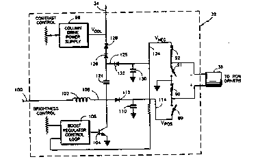
Fig. 4 is a block diagram of the improved power
supply of the present invention. ~his improved power
10 supply requires only one row power supply from which
both the positive and negative row voltage signal values
Vpos and Vneg are derived. The power supply receives an
unregulated dc ~oltage signal on a line 100 which is
input to an inductor 102. A transistor 1~04 operates as
15 a switch under the control of a pulse width modulated
boost regulator 106. While the transistor 104 is in
saturation (analogous to a switch being closed) energy
builds in the inductor 102, and when the transistor 104
is switched into cutoff (analogous to the switch
20 opening) energy is transferred fro~ t~e inductor 102
along a line 108 to capacitor 110 via a diode 112 to
provide the voltage signal VpOs on a line 114. The
capacitor 110 and diode 112 operate to filter and peak
detect the signal on the line 108 and provide the dc
25 signal VpOs on the line 114. T~e switches 89-92 control
the voltage measured across lines 114,134 in the same
manner as disclosed hereinbefore with respect to Fig. 3.
~s known in the art of power supply ~esign, the
magnitude of t~e voltage signal VpOs on the line 114 is
30 determined by the ratio of time (i.e., the duty-cycle)
W094/0l855 PCT/US~`
3Q~3
v - 10 -
the transistor 104 is in saturation. As a result, VpOs
can be expressed as:
Vpos = Vi~ / [1 - (TOn/(Ton + Toff3~] Eq. 1 ~;
where: Ton = the % of time transistor 104 is in
saturation;
To~f= the % of time transistor 104 is in
cut-of f: and -~
Vin = the signal on ~he line 100.
Fig. 5 is a plot 116 of voltage on the line 108
(Fig. 4) as a result of switching the transistor 104 :`:
between cut-off and saturation. Voltage is plotted
along a vertical axis 118 and time is plotted along a
horizontal axis 120. Voltage on the line 108 (Fig. 4)
varies along a line 122 to create a square wave ha~ing a
minimum voltage of the transistor saturation voltage
Vsat (e.~, 50 millivolts), and a maximum of (Vposl0.7
vdc3 whexe the 0.7 vdc represents the ~orward voltage
drop across the diode 112. To maintain a constant
voltage VpOs on the line 114, the regulator 106 controls
the duty cycle of the square wave signal on the line
108.
Referring again to Fig. 4, along wi~h transferring
energy to the capacitor 110, energy from the inductor
102 is AC coupled by a capaci~or 124 along a line 125 to
diodes 126,128, and ~o a capacitor 130 which is charged
~hrough diode 132 to provide the voltage signal Vneg on
a line 134. The capacitor 130 and diode 132 filter and
peak detect the signal on the line 125 and provide the
dc signal value Vn~g on the line 134. Diodes 126,128
clamp the positive transition of the signal on the line
125 to the value of the signal VCO1 on the line 34. The
present invention is best understood by deri~ing the
WO94/018S~ 2~ ~7~o~ PCT/US93/06244
equation for the signal vneg on the line 134. First
write the equation for the differential voltage on the
line 108:
Vl = Vpos + Dl - V t Eq. 2
S where: V~ s differential voltage on the line
108;
VpOs ~ ~oltage on the line 114; ~:
Dl ~ voltage drop across diode 112; and
VSat = transistor 104 satura~ion voltage.
The equation for the differential voltage on the line
125 can be written as: -
V2 = VCO1 + D2 + D3 - V Eq. 3
- where: V2 = differential voltage on the line
125; -
VCO1 s voltage on the line 34;
D2 = voltage drop across diode 126; and
D3 - voltage drop across diode 128.
The equation for voltage signal value Vneg on the line
134 can be written as:
V - -V + D Eq. 4
where: D4 = voltage drop across the diode 132.
Substituting Eq. 3 in to Eq. 4 yields:
Vne~ = -(Vcol + D2 + D3 Vl) 4 Eq. 5
Now substitute Eq. 2 into Eq. 5, which yields:
WO94/0185~ PCT/~ -
~ 3~~ - 12 - ~
Vneg = -vcol-D2-D3+(vpos+Dlovsat) + D4 Eq. 6
Assuming all the diode voltage drops are equal, the
expression for Vneg can be written as:
V = VPs ~ (Vcol + Vsat) Eq. 7
As a result, Eq. 7 demonstrates that the voltage signal
value Vneg on the line 134 is e~ual to VpOs less the
colu D voltage signal value Vcol on the line 34 and the
saturation voltage of the transistor 104, assuming the
voltage drops across the diodes are equal. Thîs
demonstrates that as VCO1 varies Vneg is automatically
compensated.
Furthermore it is found in practice that if Vsat is
less than fifty millivolts and the diodes ara all
matched to within fifty millivolts, the worst case
offset that will occur between the actual and desired
- row voltages is 150 millivolts.
Having observed the details of the operation of the
improved power supply in Fig. 4, attention is drawn to
the simplicity of the power supply of the present
~ invention for driving an symmetrically driving EL panel.
- In addition, the variation in VCO1 is automatically
compensated for while maintaining the ideal difference
between VpOs and Vneg to within 150 millivolts. The
overall power supply ef~iciency is also improved since
only a single switching regulator is required to
generate both the positive and negative outputs
pO5~vneq-
It should be understood the present invention is
not limited to the specific embodiment herein, nor by
the exemplary voltage values disclosed herein. Rather
one of ordinary skill in the art will recognize
variations of the exemplary power supply of the present
WO94/018~ 2 1 ~ 7 i~ :~ PCT/US93/06244 -
- 13 - ~
invention for providing a symmetric drive for an EL ~:
panel. AS an example the diodes may be replaced with
properly designed transistor networks, and active ~:
components may be used to replace several of the passive ::
devices illustrated in Fig. 4.
However the foregoing changes and variations are :
irrelevant to the invention, it suffices that a
symmetric drive for an electroluminescent display panel
is provided by a power supply system having a single
switching regulator from which two voltage signal values
of opposite polarity Vpos,Vneg are generated. The power
supply system~also automatically corrects the voltage
difference between Vpos,Vneg as a function of variations
in the maximum column driver voltage VCO1.
Although the preæent invention has been shown and ~
described with respect to a best mode embodiment - :
thereof, it should be understood by those skilled in the
art that various other changes, omissions and additions :
to the form and detail thereof, may be made therein
without departing from the spirit and scope of the
present invention.
We claim: