Note: Descriptions are shown in the official language in which they were submitted.
WO ~3/2595~ 2 1 3 7 ~ 3 ~ PCI /US93/05648
PORTABLE DATA PROCE5SOR WHICH SELECTIVELY ACTIVATES AND
J~ ' DEACTIVATES INTERNAL MODULAR UNITS AND APPLICATION PR~CESSOR TO
~si~ CONSERVE POWER
. .~
BACKGROUND OF THE INVENTION
This invention relates generally to portable
data collection and data processing apparatus, and
more particularly to microprocessor operated
circuits for controlling the operati~n of such
apparatus.
Portable, hand-held electronic data processing
units have taken on an increasingly significant role
in business control systems. Battery powered,
hand-held data collection terminal units are used
for inventory control in warehousing and
merchandising operations. Other uses of such
terminal units include invoicing, delivery route and
order taking operations, and fast check-out and
return control in automobile rental operations.
Portable terminal units may typically include radio
communications modules which maintain a real time
communication link with a host computer and hence
with a comprehensive business system.
Certain limitations affecting the use of these
terminal units relate to communication route
loading, namely to the limited number of terminal
units which may conveniently become linked to a host
- over the same communication channel, or at best over
a limited number of channels. Multiplexing and time
slot access protocols typically establish upper
~ limits for the number of data terminal units in any
j one system. To accommodate a larger number of
terminals within any one system radio access becomes
a premium. Data manipulation and compression prior
to transmission and on-board data storage may be
.'! .
<
.`;J
. .
2~7~3 ~
W093/2~95~ PCT/US93/05~8
implemented to increase data transmission rates and
reduce access requirements. Typically, increased
data processing capabilities are also accompanied by
~ comparative increases in power consumption. In a
J 5 hand-held, portable data collection and processing ~-
terminal an increa~ed power consumption is, however,
undesirable because of a resulting shorter operating -~
cycle between battery recharge operations. Power
saving improvements for such hand-held units are 1
lQ therefore highly desirable and are the subject of
development effort. -~
Many diverse uses of hand-held terminal units -
or apparatus in present day business systems wo`uld
ideally require a great number of distinct models of
the terminals, each having a specific configuration `
tailored to one of the many particular uses. When --
changes in the hardware configurations of data
collection terminals are implemented to meet
specific needs, the manufacturing costs of the
respective terminals tend to increase unreasonably.
It has been attempted to reduce manufacturing costs
due to model chanqes by providing functional modules ~;
which may selectively be used in distinct
combinations to make up various models of a data
collection and processing terminal apparatus.
However, interconnecting modules in a number of
different combinations tends to increase problems of
communication among the selected modules. A
particular problem relates to a decrease in product
reliability when a great number of specialized data
connections are needed. Simplification and further
improvements are desirable to electrically couple in
a simple manner any of a great number of
combinations of functional modules for different
¦ 35 models of portable data collection and processing
I terminal units.
¦ Typically, the hand-held terminal units are
;~ controlled by microprocessor devices which operate
`.~.~1
W093/25955 2 1 3 ~ ~ 3 ` PCT/VS93/05~8
under the control of stored programs. Such devices
~ are ideally suited for controlling various data
-j processing operations. In general, microprocessor
~A controlled operations of data terminal units involve
S data Input-Output (I/O) functions including
displaying information on a screen, transmitting
data messages by radio, receiving data inputs from
, data scanners or bar code readers and responding toj keyboard inputs. Microprocessors also perform
internal control functions such as monitoring power.
Data processing operations or manipulations involve
sorting, storing and retrieving both text and
numerical data, as well as updating and controlling
information in data bases. Popular data terminals
aIso make use of various prompts and menus which may
appear in a number of stacked levels. The speed of
presenting updated menu information, requested data
or other written instructions is considered a
significant element in rating the performance of a
; 20 data terminal unit. Although it is desirable to
provide more powerful microprocessor functions to
increase user friendliness by faster processing
- speeds, a resulting increase in power requirementsfor such more powerful microprocessors negates the
feasibility of such improvements.
It is known in the art to use two or more
microprocessor devices for more complex control
operations. The processors typically operate in
parallel, speeding up operations while maintaining
comparatively lower cloc~ speeds. Complex
operations are thus completed at any given clocking
i rate in a relatively shorter time than with a single
I processor. A power increase due to an added
j microprocessor is offset by the greater computing
¦ 35 power implemented without the need to drive a single
microprocessor at a higher speed or to use a single
microprocessor of a more complex architecture.
However, portable data terminal units which require
~,
21~7S3~
W093~2~95~ PCT/U~93/05~8
-- 4
extended operating time before having their power
i units recharged typically would not employ such
multiple microprocessor enhancement.
To improve the usefulness of state-of-the-art
¦ 5 portable, hand-held data collection terminal units,
it would be desirable to implement further power
saving circuit structures and operations
. and to provide interconnections among modules which
¦ are simple and reliable. Such improvements are seen
as minimizing the cost of providing specialized
; configurations of data collection terminals,
providing greater versatility and greater user
friendliness.
''',
..,
W093/25~5~2 1 e~ 7 ~ 3 ~ PCT/US93/05~8
SUMMARY OF THE INVENTION
It is therefore an object of the inventi~n to
j provide a power efficient control circuit for a
- portable data collection terminal or data terminal
5unit.
A further object of the invention is to provide
a reliable communication method and apparatus among
various functional sub-units of the data collection
terminal unit.
10It is a particular object of the invention to
provide for high speed serial communication among
various functional sub-units of the data collection
terminal unit.
Another object of the invention is to provide a
15control circuit which minimizes idle clocking cycles
of power intensive microprocessor control and data
processing elements.
A further object is to speed up response time
to input, output and data display demands on a data
20terminal unit without a typical resultant increase
in power consumption of such terminal unit.
In describing the invention, terms are given
their typical meanings, the following definitions of
which are believed to fall within these most
~5commonly understood meanings. A microprocessor
device is a control device capable of executing a
se~uence of logic instructions at a speed of
operation determined by the frequency of clocking
signals applied to the microprocessor. A memory or
30storage device may be a RAM (Random Access Memory),
either volatile or nonvolatile, a ROM (R~ead Only
Memory), or any of a number of available
electrically programmable and erasable and otherwise
~permanent storage devices. Data are one or more
numerical quantities or constants of predetermined
value, representing individually or in combination
' intelligence or information. Data may be transferred
over digital signal lines as binary signals, or as
:i
, . .
2137~
W093/2S95~ PCT/US93/05~8
radio frequency signals by RF transceiver units, or
the data may be stored in storage cells~ either
temporarily or permanently, in typical storage
devices or memories. A program is a sequence of
I 5 logic instructions which, when applied to a
-I microprocessor, control the operations of the
microprocessor. An application program typically
denotes a specific program consisting of a series of
logic instructions which control the operations of a
microprocessor in its manipulation, operation on,
and routing of data by the microprocessor, as well
as the generation of predetermined control signals
or signal sequences at certain defined points in any
operational cycle. The control signals may be
applied according to selected program instructions
ts control, among other things, the terminal
intelligence or operational sequences of the data
terminal unit.
Acc-ording to the invention, data communication
and processing apparatus comprises a plurality of
functional sub-units or modules. Selected ones of
such modules include a communication and control
device. A high speed data communication bus links
the communication and control devices in each of the
modules.
According to a more particular aspect of the
invention the data communication and processing
apparatus includes a base terminal unit which
includes a first microprocessor element or device
which is particularly dedicated to processing data.
A selective activation of the data processing device
or application device is controlled by the
communication and control device of the base unit.
The application ~lement becomes deactivated during
, 35 idle periods and its activation is initiated by the
I communication and control device upon receipt of a
,' control signal indicative of the occurrence of an
,,~
W093/259~5 2137~ ~ PCT/US93/0~
event which requires data processing operations on
data as a result of the event.
A more general aspect of the invention includes
' at least one communication and control processor
; 5 device and a separate intermittently operable data
i processing element which is controlled by at least
one communication and control processors.
Accordingly, a specific aspect of the invention
includes an apparatus, including a microprocessor
control circuit for use in data processing apparatus
which includes a first microprocessor device which
is dedicated to data processing opera1ions. A
second microprocessor device controls data inpUt and
output sequences of the data terminal unit and
controls a selective application of processed data
to or from the first microprocessor device to or
from data output or input devices of the apparatus.
The microprocessor control circuit is characterized
in that the second microprocessor also controls the
duty cycle of the first microprocessor device and in
that the first microprocessor is operational for
substantially less than fifty percent of an averaged
period of operation of the control circuit.
According to a particular combination the first
microprocessor device may be a relatively more power
intensive element, such as a 16 bit microprocessor
and the second microprocessor device may be
operational with relatively less power, such as an 8
bit microprocessor. The first and second
microprocessor devices may be advantageously coupled
to communicate through a parallel communications
interface for transferring data between the two
devices in response to interactive trigger or
handshake signals. According to a particular
; 35 feature of such combination, the first
microprocessor device operates at least at twice the
speed of the second microprocessor device and the
second microprocessor device disables the first
'` '1
` 213753i
W093~25~ PCTtUS93/~8
microprocessor device after it has completed any
'~ particular operation and has communicated its
completion to the second microprocessor device. ~-~
Particular power saving features and advantages
of such combination of the first and second
~, microprocessor devices reside in the relatively less
powerful device controlling and selecti~ely turning
on and off the more powerful first device which
~- operates at a substantially higher clocking rate
than the controlling second device. One of the
advantages of the resulting intermittent operation
of the first device is a power reduction with
respect to a microprocessor control circuit having a
continuously operational single device for providing
a similar rate of screen updates, menu displays and
data base manipulations.
Other features and advantages will become
apparent from the following detailed description,
which may be read in reference to the drawings.
., ~
wo 93/2sgs5~ 1 ~ 7 ~ PCI`/I~S93/056~8
g _ :
BRIEF DESCRIPTION_OF THE DRAWINGS
FIG. 1 is a schematic pictorial representation
of a modular data collection terminal unit to which
the present invention applies and showing
, 5schematically physical representation of modules of
the data collection terminal.
FIG. 2 is a schematic diagram of functional
interfaces among various modules of the data
collection terminal shown in FIG. 1.
10FIG. 3 is a schematic diagram of a control
microprocessor, illustrating data bus terminals for
synchronous communications.
FIG. 4 is a sequencing diagram showing
schematically occurrences of a module-initiated
15communication sequence in accordance with features
of the invention.
FIG. 5 is a further sequencing diagram
illustrating schematically occurrences of a
- controller-initiated communication in accordance
20with features of the invention.
,.,j
.~ , . . ~ -
21~7~3~
- WO 93/25!~5~ PCr/US93~05648
(. -- 10 --
'. DETAILED DESCRIPTION OF THE INVENTION
j Functional interconnections and power saving
features of the present invention may be better
1 understood from knowing how various building blocks
¦ 5 or modules of a portable data collection terminal
-' unit relate to each other. FIG. 1 shows a schematic
arrangement of various physical modules or
components that become integrated into the portable
data terminal unit which is designated generally by
the numeral 10. Hand-held terminals are of
generally rectangular, elongate shape for accepted
practical user friendliness, thus the modular
terminal unit 10 desirably has an elongate,
rectangular shape. An upper module 12 provides a
sensory or physical interface to an operator of the
terminal unit 10. The module 12 is referred to as a
keyboard and display module 12 and features a
keyboard 14 which may be a typical alphanumerical
keyboard 14, including also function keys and cursor
manipulation keys as part of an integrated keyboard
arrangement. The keyboard 14 may be, and desirably
is, a submodule 14 in itself, inserted and mounted
into a mounting frame 15 of the keyboard and display
module 12. In a typical manner, the depression of
molded keytops 16 generally closes electrical
contacts in a lower contact plane (not visible) of
the keyboard 14. The type of keyboard 14 is,
however, not critical and not considered limiting to
the invention. The keyboard being a selected one of
a number of available keyboards 14 is, however
pertinen~ to the invention. For example, in one
application the keyboard may be preferred to be a
twenty or a twenty-four key keyboard 14. Such a
i keyboard 14 comprises comparatively few keytops 16
the locations and functions of which are more
readily learned and accepted by an operator. Such
keyboards typically do not have alphabetical key
functions. Thus for many record keeping and
s'
~;.
.~,
2 1 3 7 ,~ 3 !~
~~ W093/25955 PCT/US93/05~8
merchandising operations, the keyboard 14 having an
array of twenty or twenty-four keytops may be most
. d~sirable. In another operation, a greater number of
~ keytops 16 may be required to display the letters of
-~ 5 the alphabet, numbers, and to provide keytops 16 for
~~~ the execution of various functions. Thus, a
keyboard 14 having an array of fifty-six keytops 16
may be preferred for example. Numerous variations
! in the arrangement of the keytops 16 within the
array of the keyboard 14 are additionally possible.
Mechanical or touch sensitive keytops 16 may be
employed. In fact, touch sensitive keyboards which
are known in the art, and which typically involve
programming and bi-directional feedback, may be
improved by interconnection features of the present
invention which will become apparent from the i~
detailed description as a whole.
The keyboard and display module 12 further
includes an upper cavity 17 wherein a display screen
- 20 18 is disposed. The display screen 18 is preferably
a state-of-the-art liquid crystal display, the
liquid crystal display t"LCD") technology being well
established in the art. "User friendliness" and -
versatility of the display ideally calls for a
dot-addressable liquid crystal array screen 18 which
permits the display of various alphanumeric
characters and also permits the display of graphic
symbols as well as display of Chinese or Japanese
character symbols. Of course, dot-addressable
graphic representations are known to require a
substantial level of data processing and memory
storage to permit the symbols to be displayed or
moved about on the display screen 18 with reasonable
, ~ speed. Long delays between the time that an
- j 35 operator pushes a keytop 16 to obtain data and the
time that the requested data are displayed is
considered "user unfriendly" and is commercially
~ undesirable. A display technology which has become
,,,,~ .
~;3
~1 :
2~ 3~3~
W093J259~ PCT/US93/OS~8
- 12 -
a standard is referred to as VGA technology. VGA
screens are capable of fine gray scale or color
' resolutions. The display screen 18 would be part of
a selected display screen module 19 of a number of
,~ 5 available display screen modules. FIG. 2 refers to
"~ a display screen module 20 which is similar in
function, yet which may included selected
differences to illustrate the advantages of the
modular concept in combination with other features
. 10 of the present invention. Display screens may vary
in size or resolution or both, such that options
among a number of display screen modules 19 may be
,made available to a potential user of the terminal
unit 10. A display of an array of (128 by 240)
pixels of, for example, (0.25 X 0.25~ millimeter is
an example of what is considered to be a desirable
display screen resolution. Another screen array
si,ze may be (64 X 192) pixels, for example, of (0.35
X 0.50) millimeter per pixel.
The keyboard and display module 12 occupies
most of the area of the terminal unit 10 which faces
an operator when the terminal unit 10 is held and
operationally used by the operator. Assembled to an
underside 21 of the keyboard and display module 12
are preferably two major modules of the terminal
unit 10. A first module is what is referred to as
the terminal module 22. Whereas the keyboard and
display module 12 is the major interface component
between the operator and the terminal unit 10, ~the
terminal module 22 is a major functional component
of the terminal unit 10 itself, as will become
apparent from the description herein. The terminal
module 22 functionally controls the interaction of
- the various units or modules as described herein,
and functionally is the control unit 22 of the
, terminal unit 10 as a whole. The terminal module 22
houses functional submodules and microprocessor
circuits. A significant, and also space consuming
.,
.:~
2137~3~
~ W0~3/25~55 PCT/US~3/OS~8
component is, of course, a power pack module 23.
; The power pack module may contain, for example six
AA type rechargeable cells which may be arranged in
a convenient flat arrangement and fitted into a
, 5 battery end 24 of a housing 25 of the terminal
module 22. The power pack module 23 supplies the
power to various modules of the terminal unit 10,
thus providing the capability for portable use of
the terminal unit 10.
From the above description of potential choices
of the type of display on the display screen 18, and
further choices among keyboard arrangements of the
keyboard 14, different requirements for electronic
support circuits are indicated. One of the
requirements in the support of changing functions
economically is a means to provide a ready change in
programmability of microprocessor circuits. Some
module selections of the terminal unit 10 require
less memory usage and dif~erent operational
protocols than others. In accordance with a
preferred embodiment, a memory module 27 may be -~
selected as one of a number of differently
programmed memory modules 27. However, in addition
to being differently programmed, an alternate memory
module 28, as shown in the functional diagram of ~`
FIG. 2, may include a different memory size (in cell
numbers and in configuration). The terminal module
22 may further include an exchangeable memory card
30. The memory card 30 may be used to provide
additional memory capacity as well as control
~ programs for various desired functions of the
i various modules as described herein. The memory
card 30 is schematically shown as being insertible
I - laterally into a slot 32 of the housing 25 of the
¦ 35 terminal module 22. However, the shown physical
I arrangement is but one of a number of equally
! desirable arrangements. Environmental protection of
modules of the terminal unit 10 may desirably
' ..
, .
~ 1 37S~
WOg3/25955 PCT/US93/05~8
- 14 -
suggest an enclosed and~ sealed arrangement for the
memory card 30.
i A peripheral I/O module 34 is shown in one of
! the two l~ngitudinally opposite ends and is
¦ 5 disclosed as beiny located at a lower or inner end
¦ 35 of the terminal unit 10. The inner end 35 is
¦ typically pointed toward an operator of the terminal
¦ unit 10l as the unit is held in the operator's hand
I with the keyboard and display madule 12 directed
¦ 10 upward toward the operator. The I/O (Input-Output)
module 34 may typically include externally of a
housing 36 a standard RS-232 and RS-485 connector
37. FIG. 1 also depicts a round communication
connector 38. The peripheral I/O module 34 provides
an interface between the terminal unit 10 and such
diverse peripheral devices as "docks" which are
batch transfer devices for accumulated data and
hattery charging devices, and cables which may
connect to a code scanner, for example. The RS-232
interface may typically also become connected to a
printer, for example. All these peripheral devices
- (not shown) are well known and are not part of the
invention.
At a longitudinally opposite outer end 40 of
the terminal unit 10, a serial I/O and scan
connection module 41 may be attached. The scan
connection module 41 is a high speed serial data
communication module 41 which provides for serial
data to be received in high volume from a scanner
for example. Scanner data are typically received in
a high density data string and require significAnt
processing. As will become apparent from the
further detailed description, a direct communication
j link to the data processing capability of the
1 35 terminal unit 10 is provided through the scan
connection module 41.
A further functional module of some
! significance is a communication module 44. Again in
.
~ ' :
``
213~
~ W093/25955 PCT/US93/05~8
- 15 -
reference to FIG. 1, the communication module 44 may
be disposed adjacent the terminal module 22 toward
, the outer end 40 of the terminal unit 10. The
communication module 44 is selected from a group of
~ 5 available communication modules of distinct
-' functions. The selection of one of the
communication modules such as the communication
module 44 in FIG. 1, may characterize or classify
the operation of the terminal unit 10. For example, ~
a communication module 44 may have been selected -
from a group modules which include standard FM data
radio transceiver modules, spread spectrum radio
transceiver modules, modem communication modules, -~
scanner devic~ modules, or other data input devices.
FIG. 2 shows a communication module 45 as an
alternate to the physical representation of the
communication module 44 shown in FIG. 1 to indicate
a diversity of modules available for substitution.
In further refere~ce to FIG. l, the communication
module 44 is shown as having an antenna 46,
indicating the selection being a transceiver unit
for radio frequency real time communication with a
data system. Such a data system includes typically
a further transceiver station, not shown, with which
the transceiver module 44 communicates. The second
transceiver station as a receiving end of a link is
not shown as it is commonly understood that
communication is the transfer, the transmission or
reception, of information or data over a
communication link established between two points.
The operator of the terminal unit lQ also
' constitutes a second end of a communication link
! that is established by the operator's manipulation
~ of the keyboard 14 and by the operator's visual
perception and recognition of the data displayed on
~ the display screen 18. Thus, the term
;; "communication" is understood as linking the modules
~ to other units. The presence or absence of the
.~ ~
:: `
213 S~
W093/25955PCT/US93/05~8
- 16 -
other units is of little significance to the
teachings of the present invention. These external
. units are therefore not shown to better emphasize
~,- the features of the invention.
i 5Referring now to FIG. 2, there is shown a
, functional schematic diagram of a combination of the
physical modules discussed with respect to FIG. 1 or
of alternate equivalents of the modules in FIG. 1.
The modules with respect to which preferred physical
10positioning was discussed in reference to FIG. 1 are
now shown functionally related in FIG. 2. The
terminal module 22 clearly appears as a central
functional device. It is to be noted that the
schematic representation refers to functional or
15communication rather than electrical connections.
The power pack 23 is typically coupled to power all
electrically driven circuits of the terminal unit
10. The power pack 23 is functionally and
ph~sically coupled to the terminal module 22. While
20electrical power is distributed from the power pack
23 to all electrically powered or controlled modules
of the terminal unit, the remaining power of the
power pack is actually monitored by a function of
the terminal module 22. The power pack 23 as the
25sole portable power source for the terminal unit 10
would, but for power saving provisions, experience a
-significant power drain during the operation of the
terminal unit 10.
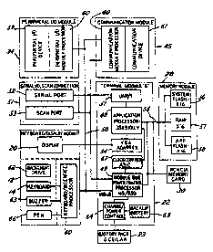
Power savings are implemented in a manner which
30typically implies a greater usage of power but which
enables power savings by more selectively using
circuit functions as they are needed. Accordingly,
- the terminal module includes preferably first and
second microprocessors 48 and 49, respectively. The
35first microprocessor 48 is a data processing device
and is also referred to herein as an application
processor 48. The application processor may be any
of a number of available microprocessors available.
s, :,
, :
~~~ W0~3/25955 2 1 ~ 7 ~ 3 .~ PCT/US93/05~8
- 17 -
Desirably the application microprocessor ~8 has the
capabili~y of processing data with greater word
length or word width than the second processor 49.
I The term word width refers to the number of data
-~ 5 bits that are capable of simultaneously being
;
-~ processed, retrieved or stored. The applicationprocessor 48 is therefore one capable, for example,
. of processing a 16-bit or a 32-bit data word. The
! processing spe`ed and clocking rate would desirably
exceed those of the second microprocessor 49. At
present, the more powerful microprocessor, such as
the microprocessor 48, also has a higher power
requirement than the second microprocessor 49.
However, even with the high power requirement during
operation, power savings may be achie~ed by
providing a rest state at which the microprocessor
48 is, for example, not clocked and thus
deactivated.
The second microprocessor 49 is also referred
to as a control processor 49. The second
microprocessor controls the operation of the
terminal module 22 and controls communication within
the terminal module as well as among the various
other modules of the terminal unit 10. Desirably,
the control processor 49 does not have the
operational power requirement as the application
processor 48 for reasons that will become apparent.
Control is an ongoing function. Although the
operational speed of the control processor 49 is
comparatively slow with respect to that of the
-application processor 48, the operational power
- consumption of the control processor 49 is also
desirably lower than that of the application
I ~ processor 48.
-I 35 A presently preferred device for the control
¦ processor is of the characteristics that are
I presently found in a Hitachi H8/330 type
; microprocessor device. The Hitachi H8/330 processor
, .~.
.--..~
2137~3~
- W093/2~955 PCT/US93~05~8
- 18 -
features on-board memory which is convenient for its
intended operation as will be seen in reference to
its operational modes as set forth herein. The H8
i ty~e processor is an 8-bit processor, capable of
processing data in an 8-bit word length. However,
~ .
the control processor need not be an 8-bit
processor. In general, the word width processing
capacity of the control processor 49 would be chosen
' to be rPlatively less than that of the application
processor 48. The control processor 49 does not
require the processing speed that is desirable for
the application processor 48, and, accoxding to the
state of the art, processors with relatively low
word width processing capacity (considering
processors in general) require less processing
power. It is to be understood, however, that the
specification of any particular device, such as was
done with the Hitachi H8-type microprocessor for the
control processor 49, is for illustrative purposes
only. Continual development efforts in
microprocessor architecture is expected to result in
various commercially available devices that may be
of equal or better utility than the specified
exemplary devices. The features and desired
functions of the invention will be helpful to one
skilled in the art to select any of a number of
acceptable devices to function in the desired manner
as described herein.
FIG. 3 shows a schematic block representative
of signal terminals of the control microprocessor 49
whish are pertinent to the preferred mode of
implementing the present invention. In describing
the significant signal and data terminals, a bar
above a designation indicates a signal low being the
active state of the signal. In the specification
t hereof the inverse or signal low active state is
! described with an N' preceding the letter name at
the respective signal term. ~
. : .-
~~ W093/2S955 2 1 3 7 ~ ~ I PCT/US93/05~8
To communicate among the various described
modules, four signal leads of the control processor
49 define the leads of a communication bus 50
~ referred to herein as "MBUS". The MBUS 50 is a high
j 5 speed synchronous serial data signal bus which may,
~, and preferably does, operate at a signal rate of 500
kilo bits per second. Better reliability of data
transfer is achieved by using the high speed data
bus. In a modular structure in which the modules
are readily uncoupled and reconnected to permit
convenient changes during the manufacture of the
~inal product of the terminal unit 10, the
reliability may be noticeably affected by
interconnection faults. When reliability decreases
with each additionally coupled module, the
advantages of modular structure are quickly
dissipated. In contrast to typical parallel data
buses used to link components of electronic products
or systems, the present system architecture of the
modular terminal unit 10 significantly reduces the
number of contacts needed to interconnect the
various modules.
Reliability might be further decreased by
electrical noise and interference coupled into the
interconnected signal lines. With fewer signal
lines to manage, it becomes feasible to protect each
line from noise and interference effects by using
well known shielding, impedance reduction and
termination techniques. Thus, the system of the
present invention provides greater reliability than
- - modular systems with conventional parallel data
transfer.
FIG. 3 shows a four signal terminal which
~ ~ constitutes the MBUS concept. "MCLK" is the
¦ 35 clocking signal which synchronizes the modular
counterparts of the control processor 49. The
clocking signal provides for a bit rate of 500 kilo
; bits per second. The terminal labeled "MTXD"
. ~:
.
~ ` ~
- 2137~
W093/25955 PCT/US93/05~8
- 20 -
transfers data from the control processor onto the
MBUS 50. The terminal labeled MRXD receives data
from other modules over the MBUS 50. The low signal
active "NMATT" is a control signal line which
~ 5 indicates that data will be communicated over the
-~ MBUS 50. These four lines effectively permit the
various modules to communicate among each other.
A number of signal contention protocols are
available and are commonly known for resolving
potential collisions in data communication. Any of
the various contention protocols will suffice to
resolve priority conflicts when data are to be
transferred among the various modules. It is to be
understood that any standard conflict resolution
- 15 procedure also may be modified if so desired to
assign specific priorities for communication among
the modules. For example, data received from a
scanning operation may be accepted and processed on
a priority basis. Keystroke inputs from the
keyboard and display module 12 may be given priority
over data flow from the communication module 45.
Similarly data messages received via radio
tr~nsmission from an external master unit (not
shown) may be given priority. Program altering
instructions may be embedded within a data message.
The embedded instructions may affect future
operations that are about to be received from one of
the modules. -
Further with respect to FIG. 3, corresponding
data lines interfacing with the application
processor 48 are indicated as parallel signal lines
DB0-7 and data lines A0-3. Data communication and
control procedures between the control
~ microprocessor 49 and the application processor 48
-¦ 35 are further described with respect to alternate
¦ embodiments.
¦ The application processor 48 is coupled to an
~ asynchronous device or "UAR/T" function 51 with an
,..~.
~-'
~~ W093~25955 2 1 3 7 ~ 3 ts P~T/US93/05~
- 21 -
: output coupled to a serial port 52 of the serial I/O
scan connection module 41. The serial I/O scan
connection module 41 further includes a scan port 53
which links to the control processor 49 and enables
i~ 5 it to communicate control signals, such as, for
; example, scan trigger signals. The application
processor 48 is further coupled to a VGA adapter
circuit or driver 54 for driving the display screen
20. The display screen function is processor
intensive. Data processing operations are,
therefore, managed directly through the application
processor 48. The data processing operations
performed by the application processor 48 are in
most instances memory-usage :intensive.
Consequently, the application processor 48 is linked
by a conventional data bus 55 directly to the memory
module 28. The memory module 28 is shown as
including representative data storage functions or
circuits including a 16-bit word width system
FLASH-programmable memory 56, a typical 16-bit word
width random access memory 57 ("RAM"), and
additional application FLASH-programmable memory 58,
also preferably 16-bit word width. The 16-bit word
width storage devices or functions 56, 57 and 58 are
preferred in conjunction with a 16-bit
microprocessor device representing the application
processor 48. Presently preferred devices may be
for example a Chips and Technologies F8680 device or
an Advanced Micro Devices 386SXLV processor. It
mu~.t be understood, however, that other devices may
exist or may become available that are ~qually
acceptable or even better suited to function as the
application processor 48. In addition, selecting a
different microprocessor 48 may result in a
different selection of memory device types, word
widths, or storage capacitites.
The peripheral I/O module 34 may, as discussed
with respect to FIG. 1, include standard connectors
~ ~ .
?':.~
2137~3i
W093J~955 PCT/US93/05~8
22 -
for coupling the module 34 to an external device. A
particular device 59 may be a portable printer
device, as shown in the function block 59 of FIG. 2,
which may be mounted or coupled directly to the
-, 5 terminal unit 10. The peripheral I/O device,
whether it is a printer, a reader, or other data
input or output device, would functionally include a
microprocessor 60. The microprocessor 60 is chosen
to interact with the MBUS system and is coupled in
each described element to function as a terminal
element, i.e., an interface communicatively coupling
the respective logic circuits of the module to the
MB~S. Thus, when the respective microprocessor
receives a communication over the MBUS 50, a
recognition of control codes may cause the
microprocessor 60 to transfer data or execute a
control instruction, which may entail activating or
de-activating the power circuits of the respective
module or conditioning the module to receive or
transmit data.
The communication module 45, which, for
example, may be a modem or any of a number of
available radio frequency transceiver modules, also
includes a compatible microprocessor 60 which
interfaces with a respecti`ve communication device 61
of the module 45. The communication device 61
would, corresponding to the desired function of the
module, be a modem or transceiver device, for
example. To be compatible with the MBUS data format
of the other described modules, the keyboard and
- display module also preferably includes a distinct
interfacing microprocessor device 60. The keyboard
and display microprocessor 60 is coupled to control
! ~ various elements which are directly associated with
the keyboard and display module 12. A particular
function that may be conveniently controlled via the
MBUS 50 and the respective control processors 49 and
60 is a backlight drive 62 function for the display
, .
2~ 378~
W093l259~ PCT~US93~05~8
screen ~0. Another function incorporates a buzzer
63. The buzzer 63 may be programmed to signal an
audible alarm as a response to an incorrect key
depression by an operator. The buzzer 63 may
further be used to alert an operator when a charge
¦ and power control circuit 64 detects that the power
3 pack 23 has become discharged and a backup battery
65 is being engaged. In addition, the power control
' 64 may function to shut down the terminal unit 10
, 10 from further operation until the power pack has been
recharged or replaced. In the preferred mode, power
from the back-up battery 65 would nevertheless be
maintained on the control processor to enable it to
determine when the power pack 23 has in fact been
recharged or replaced.
The processor 60 of the keyboard and display
module 12 may also control other input or output
devices that may be coupled to the keyboard and
display module 12. For example, a pen 66 may be
coupled to the keyboard and display module 12 for
use in connection with a pen stylus sensitive
keyboard module 14, or in connection with a pen
stylus sensitive display screen 20. In this latter
instance, the display screen module 20 becomes an
input device in addition to being an output device.
The input is received through manipulation of the
pen 66 by an operator.
The application processor 48 and the control
processor 49 are preferably controlled through a
timing Application Specific Integrated Circuit 67
("clock control ASIC"). The clock control circuit
67 may be driven from a single clock signal which is
then divided to provide respectively different
~ clocking rates to each of the processors 48 and 49.
l 35 The implementation of the timing circuit 67 in a
I single circuit function is more efficient and
provides synchronization among the components and
. ~1
~13r?~3 ~
W093/259~5 PCT/US93/05~8
- 24 -
modules. A second clock signal for implementing a
real time clock may be provided.
j In addition to the reliability advantages of
~ coupling modules via the four-line MBUS mentioned
--¦ 5 above, the MBUS 50 also provides a space saving
advantage, l.e., morP compact physical routing of
~ cables among the modules.
¦ Power savings which are obtained through the
~¦ control of the functions of the various described
! 10 modules via the MBUS 50 will be best understood from
the following description in reference to FIGS. 4
and 5. To conserve power and prolong the
operational time of the terminal unit 10 between
recharges or replacement of the power pack 23, the
control processor 49 and the related MBUS module
processors 60 perform a special power-saving control
function: any module which is not in active use is
placed into a dormant state.
The MBUS 50 communicatively interconnects the
modules of the terminal unit 10, such as the
peripheral I/O module 34, the communication module
45, the keyboard and display module 12 and the
terminal module 22. Other modules which in the
future may be included in the active communication
network of the MBUS 50 may simply be added as
described herein. For each module, one of the
microprocessors 60, having the data terminals of the
microprocessor 49 shown in FIG. 3 (i.e., terminals
MCLK, MTXD, MRXD and NMATT) is coupled to the
respective lines of the MBUS 50 to become part of
the internal communication network of the terminal
unit 10. The microprocessors 49 and 60 constitute
the terminal elements of the communication network
,, ~ represented by the MBUS 50. For each module, the
:J 35 respective microprocessor 60, though it may be
¦ physically identical to the control microprocessor
¦ 49, functions as a subservient processor to the
control processor 49. The microprocessors 60
,j
,~s
213~,~3-;~
.
` W093/259~ PCT/US93/05~8
- 25 -
become a communication interface between the MBUS 50
, and the functional circuits of the respective
¦ module, whether it is the communication module 45,
r the keyboard and display module 12 or the peripheral
I/O module 34. Inputs from the respective module
are accepted by the processor 60. An H8/330
microprocessor includes internal memory for
receiving and temporarily storing data
co~munications. Programmable ROM on the H8/330
' 10 permit instructions to be stored which particularly
configure the microprocessor as a ~odule processor
60. The interface operation of the microproressor
60 differs from the controlling operation of the
control processor 49 as may be realized from the
description of the interaction of the processors in
reference to FIGS. 4 and 5.
A normal state of the microprocessors 49 and 60
is a sub-active or dormant state. In this state,
the module processors 60 and the control processor
49 are clocked at a power saving "slow'l clocking
speed. The sub-active or dormant operational state
permits the module processors 60 and the control
processor 49 to execute certain long-interval
control functions, such as watching for a keytop
depression by the keyboard and display screen
processor 60 or a low battery signal to be received
by the control processor 49 from the charge and
power control circuit 64. Upon occurrence of an
event which affects the operation of any typical
communication function which is driven over the MBUS
50, all modules and the control processor are placed
, ` into a fully activated mode. The control processor
: 49 queries, directs and controls communication over
th~ MBUS 50.
For example, FIG. 4 shows an activation cycle
of the MBUS 50 which is initiated by one of the
I described modules other than the terminal module 22,
;j i.e., from one of the processors 60. The respective
.~
':
2137~3~
W093/2~955 PCT/US93/05~8
- 26 -
processor 60 drives the NMATT li~e of the MBUS 5~
into a low signal state. The low state of the NMATT
line activates all processors 60 to receive an
inquiry or instructions. At Tl in FIG. 4, all
- 5 modules have been placed into the active state.
During the time interval T1 to T2 the control
processor sends a query or polls the activated
modules over the MTXD line, which is reserved for
transmissions originating from the terminal module
22, i.e., from the control processor 49. The query
would typically contain at least one byte of data.
The quantitative translation of the byte of data
indicating to the processors 60 that it is a query
in response to one of the module processors 60
having driven the NMATT line to a low state. The
query shown at 71 signals the processor 60 to
transmit its data message over the NRXD line of the
MBUS 50. At the onset of the data transmission 72
from the respective communicating module processor
60, the NMATT line is restored to a high state,
placing all other modules back into the dormant
condition. As shown in FIG. 4, the data
communication may proceed for a variable length-of
time past the time state T2 at which the NMATT line
has returned to a high state. Upon termination of
data communication from the respective module
processor 60 to the control processor 49 the control
processor 49 sends a message 73 confirming correct
re~eipt of the data message (at T3). Again the
confirming data message contains at least one byte
of information, the decoding of which would either
indicate an error code or signal the correct receipt
of the data message. At that time (at T3), the
communicating module processor 60 and the control
-¦ 35 processor 49 also assume the power saving dormant
state.
FIG. 5 describes a very similar event in which
the control processor 49 drives the NMATT line to a
..
''I
21~7~
W~93/259~ PCT/US93/05
- 27 -
low state. Again, all processors 6G assume an active
state and receive a communication 75 of typically at
'~ least one byte of information from the control
processor 49 during the time interval between T1 and
T2. The information 75 contains an address of the
module to which a data message from the control
~ processor 49 will be directed. The respective
-~ module processor acknowledges its understanding of
the address by a responding message 76 which may be
translated by the control processor 49. In response
to the receipt of the message, the control processor
releases the NMATT line which assumes its normal
high state and places all non-affected module
processors 60 again into a dormant state. The
control processor 49 then transmits its data message
as indicated at 77 to the respective previously
addressed module processor 60. At the conclusion of
the communication 77 from the control processor 49,
the respective module processor acknowledges receipt
of the communication 77 by its response 78. On
transmission and interpretation of the response 78
that the communication 77 has been received
correctly, both the control processor 49 and the
respective module processor 60 assume their dormant
states. It is to be noted that the respective data
messages shown in FIGS. 4 and 5 indicate durations
of data messages. It is to be understood that the
high and low states of other than the NMATT line
indicate a time interval during which a great number
of high or low states in synchronous time slots are
transmitted essentially at the bit rate of 500 kilo
bits per second. This bit rate may include start and
I ~ stop intervals.
In the described communication events, power
¦ 35 consumption by the terminal unit 10 is minimized by
¦ pr~viding for a quasi dormant state for
substantially ail functions of the various modules,
such that electrical power is used in pulses during
2137~3~
W093l25~ PCT/US~3/05~8
- 28 -
- the described query states and only in spurts by
- certain modules during real time performances.
, Highly power intensive data processlng operations in
i the terminal module 22 provide further power savings
;~ S in communication from and to the various modules.
The term "data processing operation" is used
; herein to describe the manipulation of a series of
binary codes according to programmed instructions to
arrive at a desired result. Because of the great
number of discrete binary operations required to
perform many of the most common data processing
functions, higher prvcessor speeds and more complex
or powerful microprocessor circuits of those
typically available are more desirable for data
processing operations.
The application processor or data processing
device 48 may be an "Intel 80C188EB" device which is
"16-Bit" microprocessor device, operated at a
preferred speed of 9.2 megahertz (MHz). At such
preferred clocking speed of 9.2 MHz, the power
consumption or operating current consumed by the
data processing microprocessor device 48 is
approximately 55 milliamps ("mA"). The control
processor 49 is in the particular implementation a
"Hitachi H8/325l' device which is an "8-Bit"
microprocessor, operated at a speed of one-half of
the speed of the data processing microprocessor 48,
or 4.6 MHz. Because of the smaller physical size of
the control processor 49 and the slower, preferred
clocking speed, the power consumption or current
required by the control processor 49 in its
operational mode is only about 9 mA, hence less than
one-fifth of the power consumed by the processor 48.
Because of continuous advances in the field of
~ 35 microprocessors over the past decade, it is to be
i expected that in the future other microprocessors
will be marketed which will meet or exceed the
requirements of the presently preferred
~i .
;i,~
21;~7~3 ~ `
W093/2595~ PCT/US93/05
- 29 -
- microprocessors and that these microprocessors also
. may operate in accordance herewith. In general, the
control microprocessor circuit or the control
~ microprocessor 49 desirably operates at a slower and
i 5 less power consuming speed than the application
microprocessor circuit or the application
microprocessor 48. A one-to-two speed ratio for
driving the respective microprocessors 49 and 48 is
preferably chosen because of the power savings that
are realized with respect to the portable terminal
unit lO.
The clock control circuit 67 may be expanded in
its function to include an interface circuit between
the processors 48 and 49, which incorporates data
transfer as well as clocking functions. The clock
control circuit 67 would include in such coupling
arrangement a typical divide-by-two timing circuit
function. An original 9.2 MHz clocking signal port
and a signal port with the divided by two signal
would be coupled to the respective timing signal
input ports of the processors 48 and 49,
respectively, to drive the processors 48 and 49 at
their respective speeds of 9.2 and 4.6 MHz. As
already described, a second clock may be coupled to
the clock control circuit 67 to provide a real time
clock.
The preferred control processor 49 includes in
its commercial implementation, in addition to
typical microprocessor registers and an arithmetic
logic unit, such functional circuit blocks as ROM,
RAM and communications ports. According to
preferred embodiment, data communication between the
processors 48 and 49 occurs via an interface circuit
including, for example, two 8-bit data registers or
latches (not shown). It is to be understood,
however, that the control processor 49 may have a
direct bus interface provision and become directly
co~pled to the application processor 48, the coupled
r
2l3 ~
WO 93/25g~5 . . ' PCr/USg3/05648
- 30 -
; processors 48 and 49 thereby being capable of
bidirectionally passing data and control signals
-, without two 8-bit data registers or latches. Also,
data latches are ~enerally considered temporary data
storage devices. Data from one device are latched
into a respective data latch to be retrieved by a
~ second device. Therefore, in general, the operation
s of the data latches constitutes a primitive
equivalent of what is known as a dual port memory.
Dual port memories or memories which are accessed
via at least two ports are known in the art. The
substitution of the below described latc:hes with a
dual port memory in a "dàta storing int:erface" is
therefore considered to be within the scope of the
present invention. The clock control ASIC function
67 shown in FIG. 2 should be understood to not only
include the clocking signal coupling circuits to
drive the respective application processor 48 and
the control processor 49, but to further include the
data interface or bus to permit the desired
bidirectional data and control code communication
between the processors 48 and 49 as further
described herein. In further reference to FIG. 2, an
integration of the processor devices 48 and 49 into
a single device desirably may include the referred
to function of the interface and clock control
- circuit 67 as an integral part of an integrated
circuit (not shown).
Tests have shown that typical data processing
operations performed by the application processor 48
require approximately 10 milliseconds of time, and
not more than 20 milliseconds, on the average. It
, has further been found that a more user friendly and
, a more practical response time may be obtained from
¦ 35 the terminal unit 10 with less power required when
! substantially all data processing operations are
performed by the application processor 48 and the
application processor is subsequently immediately
~ W093/25955 ~1 ~ 7 ~ 3 ~ PCT/US93/OS~8
- 31 -
deactivated, than if a single alternative
microprocessor circuit were used operating at a
i higher rate and including sufficient computing
capacity to perform all required functions in an
. 5 appropriately short time. In the preferred
-I selection of the two processors, the combination of
the application processor 48 and the control -~
processor 49 amounts only to an approximate increase
in current usage of typically about ten percent, and
in the extreme, of no more than 20 percent over the
normal operating current level of the control
processor by itself. The combined power consumption
of the application processor 48, as controlled by
the control processor 49, and the control processor
49 is about one fifth of the power consumption of
the application processor 48 itself when it is
operated continuously. However, the display speed
and data manipulation speed of the terminal unit 10
essentially is the same as if the terminal unit 10
were controlled by the more powerful application
processor 48.
The operating current requirement for the
application processor 48 is directly related to the
number of actively switching elements in each
computational operation. Though having an interrupt
function, the referred to 80C188EB processor 4B does
not include, in contrast to the control processor
49, any internal memory devices. FIG. 2
consequently shows a data bus 55 of the processor 48
coupled to external memory devices, such as the
system FLASH memory 56 (functionally equivalent to a
read-only memory or "ROM"), the flash electrically
erasable and programmable read-only memory 58
("FLASH EPROM") and a typical random access memory
57 ("RAM"). The data bus 55 further couples the
application processor directly to the display module
20 ("LCD DISPLAY") of the terminal unit 10, such as
a dot addressable LCD graphic screen module, for
,~
.~.
- 2 ~ 3 ~ ~
W093/2S955 PCT/US93/05~8
- 32 -
example. A direct data transfer by the high speed
application processor 48 to the LCD screen is
preferred because of substantial amounts of data
~' handling or processing that is required in updating
; 5 a particular screen~ For example, even a small
graphic screen display, such as a screen of 48XloO
- pixels, requires that each of the pixels be updated
on a continuous basis. Typically, control circuits,
which are part of the data display function of the
module 20 and are not separately shown, and which
may be specific to a particular screen display, may
- routinely re-apply currently displayed information
dots in a cyclic refresh operation to 1he already
identified pixels of the screen. However, to update
- 15 the screen, each pixel of the screen must be
updated. This is so for any updating of the screen,
even for a simple display line scrolling operation
which an operator may not even consider noticeable
or significant. To facilitate such updating of
information in a prompt, user-friendly, and power
efficient manner, a data processing operation and
the high speed passing of the updated data between
the RAM memory 57 and the data display 20 is
performed during a short operational activation of
the application processor 48. More data processing
with respect to the data display screen 20 may be
required for routine menu operations. Menu
operations are particularly desirable for such
portable terminal units 10 because the typical user
may not be well acquainted with computer terminals.
Well defined menu operations with a number of
available menu levels are found to significantly
increase the user friendliness of a terminal unit.
An efficient menu operation is known to involve data
base searching and data retrieval in addition to the
normal display screen updating operation. The
¦ described microprocessor circuit with the
I selectively activated data processing device 48 and
..-.
~i~'
- wo93~25gss ~137~ ~ PCT/US93/05~8
~ 33 ~
the relatively smaller and slower control processor
' 49 has been found to be particularly advantageous
' for these purposes.
A selective activation and deactivation of the
microprocessor circuit portion implemented by the
data processing device or application processor 48
would also provide power savings when the operating
speeds of the two processors 48 and ~9 are the same.
.' If both processors 48 and 49 are being operated at
the same speed, however, the power savings is not as
- great as that realized in accordance with the
preferred embodiment of the described invention.
FIG. 2 shows schematically an arrangement of
electrical components of an exemplary terminal unit
10, and of the preferred interactive relationship of
such components with the application processor 48 or
the control processor 49. In the embodiment shown
in FIG 2, the appiication processor 48 controls
directly the RS-232/485 standards serial interface
34. The flash EPROM programmable read-only memory
58 is preferred to have no less than 256K byte
storage capacity. The flash EPROM may supplement or
even replace standard ROM, such as memory 56 which
is preferred to have at least a 512K byte storage
capacity. In the preferred example of the terminal
unit 10, the ROM, if usedl would provide typical and
normally non-variable data processing protocol
instructions. Such ROM may include control
instructions for standard display updating routines
as well as for other routines which are typically
implemented-by standard keyboard instructions and
I which pertain to typical data input and output
i commands.
-1 ~ The random access memory 56 is in the specific
¦ 35 embodiment a semi-permanent static RAM type circuit.
The memory may have a capacity of 512K bytes. The
preferred data storage capacity has been determined
to provide sufficient storage for an on-board data
-.
;:
,
2~37~3~ -
W093/25955 PCT/US93/05~8
- 34 -
base related to typical inventory or delivery route
type information. In view of the portability of the
; terminal unit 10, an unexpected loss of battery
i~ power may bring about a significant loss of
l 5 information unless the data stored at the time of a
temporary loss of battery power are protected from
! destruction until full battery power is restored.
-¦ For example, the terminal unit 10 may be returned at
an initial signal of "low battery" to a battery
i 10 charger unit (not shown) for a recharging operation
and any stored data may be transferred, even while
the battery 23 is being recharged, from the terminal
unit 10 to a host computer (not 16 shown in FIG. 1).
A preferred LCD display 20 is a graphic display
- 15 ha~ing an array of 48 x 100 pixels. Typical menu or
special graphic screen data may be pre-established
for a particular terminal unit 10 or for an
application group of such units and may be stored
initially in the specific ROM 56 provided for the
particular unit or units 10. As previously
discussed, the updating of displayed data on the
screen device 20 requires a significant amount of
data processing. Typically, such data processing
operations involve accessing permanently stored
screen display information, such as from the ROM 56
or from the flash EPROM 58, the manipulation of such
information, and temporary storage of such
manipulated information in the random access memory
57. As shown in FIG. 2, the application processor
48 has direct functional control over the respective
de~ices for su_h data updating manipulations with
respect to the LCD Display screen 20.
Another function that is desirable in
connection with LCD display screen 20 is contrast
control. In regards to FIG. 2, such a control may
be integrally coupled to the VGA adapter circuit 54.
The contrast of the LCD display screen 20 is
typically set and adjusted by an operator and is a
",
..
2 1 3 ~ ~ ?~ .~
~~ W093/25~ PCT/US93/05~8
- 35 -
matter of choice. The contrast may be adjusted for
example by a typical key depression or by a keyboard
sequence given by an operator. Such control input
executions are within the scope of operations of the
~ , 5control processor 49. The contrast display may be
-~~ controlled as indicated in FIG. 2 ~y the functional
' coupling of the keyboard circuit 12 to the control
j processor 49 and the further coupling of the
processor 48 to the contrast control circuit and
t, 10then directly to the LCD display screen circuit 20. .;
The LCD display screen 29 in the preferred
embodiment is equipped with the back lighting drive
62. Many warehouse operations, route delivery
operations and even merchandising inventory
15operations must often be performed under
sufficiently poor lighting conditions, thereby
requiring a backlighting source to be supplied as a
standard feature of the LCD display screen 20. A `~
preferred backlight drive circuit 62 is preferably
20coupled through the MB~S 50 to the control processor
49. A preferred backlight drive circuit for use in
conjunction with the exemplary terminal unit 10 is
described in applicant's co-pending PCT patent
application Serial No. PCT/US9208646 filed October
2512, 1992. Because an operator may wish to adjust
the backlighting (i.e., for example, its brightness
or luminescence), both the application processor 48
and the control processor 49 may interact with the
backlight drive circuit 62 to provide for an
30operator controlled brightness control sequence to
be communicated to the backlight drive 62.
-~ Besides the timing function circuits for the
real time clock and its functions, the control
circuit 67, as an ASIC, may also include the
35clocking signals to each of the two processors 48
and 49. The control circuit 67 may also provide the
`~ data communication functions between the application
processor 48 and the control processor 49 by two
~ .~;i,
i~
,r~
2l37~3~
W093/2595~ PCT/US93/05~8
latching circuits as mentioned above. Also as
mentioned above, the control processor 4g functions
to activate or "wake up" the application processor
', 48 for data processing operations. In one
. 5 contemplated embodiment the control circuit 67 may
;
-1 include integrally a switching circuit function for
- separately switching the application processor 48
off or on. Such a switching operation may be
j implemented by a typical switch as part of the
I 10 integrated control circuit 67 which selectively
interrupts and reestablishes the clocking signal to
the application processor 48. The flanction of
deactivating and reactivating the application
processor is controlled in a preferred embodiment
via the control device 67 in a somewhat different
manner. Instead of controlling the clocking circuit
to the application processor 48 in the control
circuit 67 with a control signal from the control
processor 49, the control function is preferably
split. In other words, the application processor 48
provides a shutdown status signal to the control
processor 49 and then shuts itself down. The
control processor 49 subsequently returns the
application processor 48 to an active state upon the
occurrence of any event which requires the operation
of the application processor 48.
Further in reference to FIG. 2, a trigger
control signal of the scanner module 41 may be
received by the control processor 49. However the
data flow from the scanner module 41 would be
rece ved directl-y by ~he application processor 48
for further processing and storage. Input signals
- which are received at speeds within the operational
capability of the control processor 49 are received
by and transferred through the control processor 49.
For example, key depression signals from the
keyboard 49 are preferably received directly by the
! control processor 49- A preferred keyboard size for
. .,
s`'~i
wo g3/259~5 213 7 ~ 3 ~ PCT/US93/05~8
- 37 -
the terminal unit 10 referenced herein, as indicated
j in FIG. 2, is a 6x8 key matrix. Such a size is
optimal because of space considerations and requires
that multiple functions be implemented by each of
~-~ 5 the keys. However, the selection of a preferred
keyboard remains in any case one of choice and has
no particular bearing on the teachings of the
in~ention.
Because of the "slow'~ realtime key function
selection by an operator in comparison to the ~'fast"
processing speed of even the slower control
processor, the interpretation of which key function
- has been selected may be made by the control
processor 49. An "event" indication character
communicated to the application processor 48
preferably reflects already which of the available
functions of a particular key has been selected.
- The preprocessing of relatively slow occurring
events has been found to limit the operational
periods of the application processor 48.
The control processor further controls an input
to an audible alarm circuit 63 ("BUZZER"). An
audible alarm is a "slow occurring event" which
alerts an operator of an alarm condition or signals
that a processing operation has been completed. For
example, when the application processor 48 has
received a string of data from a bar code via the
scanner module 41, and has further processed the
received information to verify its correctness, the
application processor 48 may communicate an
acceptance code to the control processor 49 and be
--~ shut down from further operation. The control
-¦ processor will then routinely generate an audible
signal to alert the operator of the acceptance of
the information. Prior to communicating the
acceptance code to the control processor, the
!. application processor may retrieve from its memory
: 57, for example, further information relating to the
213783~
W093/25955 PCT/US93/05
- 38 -
bar code information which has just been read and
~ accepted, and may compile an information screen
'; di,splaying such retrieved f~rther information to the operator prior to 'the deactivation of the
application processor 48. Thus, by the time the
'-~ operator is alerted by the audible signal that the
respective bar code information has been read and
accepted, the pertinent further information relating
to the bar code information is already displayed on
the LCD display screen 20.
Another device which is preferably under direct
control of the control processor 49 is the power
control circuit.64 ("CHARGE/POWER CONTROL") of the
terminal unit 10. A serial interface 34 may
- 15 optionally be controlled by the control processor
49. Based on the power saving interaction between
the application processor 48 and the control
processor 49, various additions of other devices or
functions to the general operation of the terminal
unit 10 may be feasible without unduly limiting the
operational cycle of the terminal,unit 10.
The interaction between the control processor
49 and the application processor 48 is described in
greater detail in reference to FIG. 2. In general,
the application processor is restricted to data
processing operations. The operations of the
control processor 49 generally pertain to
in~ut-output control functions which include
periodic monitoring functions, such as monitoring
- 30 the state of the battery 23 via the charge/power
control circuit 64. Though less powerful and slower
~ than the application processor 48, the control
'':=', processor 49 controls the activation or reactivation
i ~ of the application processor 48. However, the
.¦ 35 application processor 48 preferably processes the
¦ parameters and feeds the respective instructions by~ which the control processor is operated to the
,I control processor 49.
",i
,,,:
'~r,~
~;,
~ W093/25955 2 ~ , PCT/US93~05~8
- 39 -
Changes may be made in the selection of the
first and second microprocessor devices 48 and 49 as
application and control processors, respectively.
The described microproce.ssor devices have been found
particularly suitable for various operations that
were expected to be performed by the terminal unit
10 in the above-referred to operations.
It should be realized that, depending on the
contemplated type of portable use, various other
changes and modifications in the structure of the
described embodiment would be possible without
departing from the spirit and scope of the invention
as set forth in the claims.
:~.
,,;,
.