Note: Descriptions are shown in the official language in which they were submitted.
WO 94/27376 PCT/US94/04363
2138033
TUNABLE FILTER CIRCUIT AND METHOD THEREFOR
Background of the Invention
The present invention relates generally to filter circuitry and,
more particularly, to a tunable filter circuit for a transceiver operable
alternately to transmit or to receive modulated sign~
A communication system is comprised, at a minimum, of a
10 transmitter and a receiver interconnected by a communication
channel. A communication signal is transmitted by the transmitter
upon the tr~n.~mi~.sion channel to be received by the receiver. A radio
communication system is a communication system in which the
transmission channel comprises a radio frequency channel defined
15 by a range of frequencies of the electromagnetic frequency spectrum.
A transmitter operative in a radio communication system must
convert the communication signal into a form suitable for
tr~n~mi~.sion upon the radio-frequency channel.
Conversion of the communication signal into a form suitable
20 for transmission upon the radio-frequency channel is effectuated by a
process referred to as modulation. In such a process, the
communication signal is impressed upon an electromagnetic wave.
The electrom~gnetic wave is commonly referred to as a "carrier
signal." The resultant signal, once modulated by the communication
25 signal, is commonly referred to as a modulated carrier signal or,
more simply, a modulated signal. The transmitter includes circuitry
operative to perform such a modulation process.
Because the modulated carrier signal may be transmitted
through free space over large distances, radio communication
30 systems are widely utilized to effectuate communication between a
transmitter and a remotely-positioned receiver.
The receiver of the radio communication system which
receives the modulated carrier signal contains circuitry analogous
to, but operative in a manner reverse with that of, the circuitry of the
WO 94/27376 PCT/US94/04363
.
'2.~3~3 - 2 -
ransmitter and is operative to perform a process referred to as
demodulation .
Numerous modulated carrier signals may be simultaneously
transmitted upon differing radio frequency channels of the
5 electromagnetic frequency spectrum. Regulatory bodies have divided
portions of the electromagnetic frequency spectrum into frequency
bands, and have regulated transmission of th~ modulated carrier
sign~l~ upon various ones of the frequency bands. (Frequency bands
are further divided into ch~nnel~, and such channels form the radio-
10 frequency channels of a radio communication system. Suchchannels shall, at times, be referred to hereinbelow by the term
conventionally-defined frequency ch s~ n n els. ~
A two-way radio communication system is a radio
communication system, similar to the radio communication system
1 5 above-described, but which permits both tr~n~mi~sion and reception
of a modulated carrier signal from a location and reception at such
location of a modulated carrier sign~l Each location of such a two-
way radio communication system contains both a transmitter and a
receiver. The transmitter and the receiver positioned at a single
20 location typically comprise a unit referred to as a radio transceiver,
or more simply, a transceiver.
A cellular communication system is one type of two-way radio
commllnic~tion system in which communication is permitted with a
radio transceiver positioned at any location within a geographic area
25 encompassed by the cellular communication system.
A cellular communication system is created by positioning a
plurality of fixed-site radio transceivers, referred to as base stations
or base sites, at spaced-apart locations throughout a geographic area.
The base stations are connected to a conventional, wireline telephonic
30 network. Associated with each base station of the plurality of base
stations is a portion of the geographic area encompassed by the
cellular communication system. Such portions are referred to as
cells. Each of the plurality of cells is defined by one of the base
stations of the plurality of base stations, and the plurality of cells
WO 94127376 PCT/US94/04363
~ 21~80:~3
-- 3 --
together define the coverage area of the cellular communication
system.
A radio transceiver, referred to in a cellular communication
system as a cellular radiotelephone or, more simply, a cellular
5 phone, positioned at any location within the coverage area of the
cellular communication system, is able to communicate with a user
of the conventional, wireline, telephonic network by way of a base
station. Modulated carrier signals generated by the radiotelephone
are transmitted to a base station, and modulated carrier sign~l~
10 generated by the base station are transmitted to the radiotelephone,
thereby to effectuate two-way communication therebetween. (A
signal received by a base station is then transmitted to a desired
location of a conventional, wireline network by conventional
telephony techniques. And, sign~l~ generated at a location of the
15 wireline network are transmitted to a base station by conventional
telephony techniques, thereafter to be transmitted to the
radiotelephone by the base station.)
Increased usage of cellular communication systems has
resulted, in some instances, in the full utili~tion of every available
20 tr~n~mi~sion channel of the frequency band allocated for cellular
radiotelephone communication. As a result, various ideas have been
proposed to utilize more efficiently the frequency band allocated for
radiotelephone communications. By more efficiently utilizing the
frequency band allocated for radiotelephone communications, the
25 tr~nsmi~ion capacity of an existing, cellular communication system
may be increased.
The tr~n~mi~sion capacity of the cellular communication
system may be increased by minimi7ing the modulation spectrum of
the modulated signal transmitted by a tr~n~mitter to permit thereby
30 a greater number of modulated sign~l~ to be transmitted
simultaneously. Additionally, by minimi7.ing the amount of time
required to transmit a modulated ~ign~l, a greater number of
modulated signals may be sequentially transmitted.
By converting a communication signal into digital form prior
35 to tr~n~mi~sion thereof, the resultant modulated signal is typically of
WO 94/27376 PCT/US94104363
~ ~
-- 4 --
a smaller modulation spectrum than a corresponding modulated
signal comprised of a communication signal that has not been
converted into discrete form. Additionally, when the communication
signal is converted into digital form prior ~o modulation thereof, the
5 resultant, modulated signal may be trans~nitted in short bursts, and
more than one modulated signal may be transmitted sequentially
upon a single, conventionally-defined, frequency channel. (As more
than one modulated signal may be transmitted upon a single,
conventionally-defined, frequency channel, the term frequency
10 channel is sometimes referred to as the portion of the conventionally-
defined frequency channel during which a particular transmitter
transmits a modulated signal to a particular receiver. Hence, in a
communication scheme in which modulated signals are transmitted
in discrete bursts, two or more frequency channels may be defined
15 upon a single, conventionally-defined, frequency channel.)
As a single frequency channel is utilized to transmit two or
more separate signals during nonoverlapping time periods, a
method of signal transmission is referred to as a time division
method. A communication system incorporating such a time
20 division method of signal tr~n~rni~sion includes a Time Division
Multiple Access communication system or, more simply, a TDMA
communication system.
A TDMA communication system includes a transmitter
operative to transmit signals to a receiver in intermittent bursts
25 during intermittent time periods. Such signal transmitted to a
particular receiver operative in a TDMA communication system
shall hereinafter, at times, be referred to as a TDMA signal.
A TDMA communication system is advantageously utilized as
a cellular communication system as, during time periods in which a
30 base station does not transmit a TDMA signal to a particular
radiotelephone, other TDMA sign~l~ may be transmitted. In
particular, the radiotelephone to which the base station transmits a
TDMA signal may, in turn, transmit a TDMA signal to the base
station, thereby permitting two-way communication between the base
35 station and the radiotelephone upon a single, conventionally-def~lned
WO 94127376 PCT/US94/04363
~ 2138033
-- 5 --
frequency channel as signals transmitted to the radiotelephone by the
base station, and by the radiotelephone to the base station may be
timed to occur during alternate time periods.
As the transmitter and receiver circuitry portions of the
5 radiotelephone operative in such a TDMA communication system are
required to be operable only during alternate time periods, certain
circuitry portions of radiotelephones operable in conventional,
cellular communication systems are not required. For instance,
duplexer filters positioned to connect both the transmitter circuitry
10 portion and the receiver circuitry portion of the conventional, cellular
radiotelephone and the radiotelephone antenna theretogether, are not
required to form portions of radiotelephones operable in a TDMA
communication system as the receiver and transmitter circuitry
portions of such radiotelephone need not be operable simultaneously.
15 Rather, switch circuitry may be utilized alternately to connect the
receiver circuitry portion with the radiotelephone antenna or the
transmitter circuitry portion with the radiotelephone antenna.
Radiotelephones constructed to be operable in either a
conventional, cellular communication system or in a TDMA
20 communication system each contain filters for removing undesired
sign~ both those generated during generation of modulated signals
by transmitter circuitry of the radiotelephones and also for removing
undesired signal portions of sign~l~ received by the radiotelephones.
More particularly, the radiotelephones include both transmit and
25 receive filters.
A transmit filter is utilized to remove harmonic sign~ and
other undesired sign~l~ formed during generation of the transmit
signal by transmitter circuitry of the radiotelephone. (For instance,
during mi~ing processes in which the information signal is
30 impressed upon a carrier signal, undesired harmonic ~ign~ls are
also generated. Such undesired ~ign~l~ are filtered by the transmit
filter prior to transmission of a modulated signal by the transmitter.)
A receive filter is utilized as a broadband filter for filtering
sign~l~ received by the transceiver which are of frequencies beyond a
35 frequency bandwidth of interest. (For instance, if a signal
WO 94/27376 PCT/US94/04363
2~38033 - 6 -
transmitted to the radiotelephone is transmitted upon a frequency
channel of a frequency bandwidth of a range of frequencies
encompassed by a frequency band allocated for radiotelephone
communications, the receive filter is of a frequency passband which
passes signals of frequencies within tlie fre~uency band allocated for
the radiotelephone communications, but which rejects signals which
are of frequencies beyond the frequency band allocated for
radiotelephone communications.)
Radio transceivers operable in conventional, cellular
communication systems are operable simultaneously to receive and
to transmit modulated ~ . Hence, both the transmitter and the
receiver circuitry of such radiotelephones must be simultaneously
operable. In such radiotelephones, duplexer filters, brie~ly noted
hereinabove, are oftentimes utilized as the transmit and receive
filters. Typically, a duplexer filter is formed of a block of ceramic
material, cavities forming inner conductors of transmission lines are
formed to extend through the ceramic block, and a co~t.ing of
electrically-conductive material is formed upon at least portions of the
ceramic block. A first portion of the duplexer filter forms the
transmit filter and a second portion of the duplexer filter forms the
receive filter. Because only a single ceramic blocl~ contains both the
transmit and the receive filters, the physical dimensional
re~uirements of a duplexer filter are somewhat less than the physical
dimensional requirements of separate transmit and receiver filters.
However, when the transceiver is operable in a TDMA
communication scheme wherein the transmitter and the receiver
circuitry need not be simultaneously operable, the transmit and
receive filters simil~rly need not be simultaneously operable.
Heretofore, though, a single filter serving both as a transmit filter
and as a receive filter has not been utilized as the filter
characteristics required of the transmit and the receive filters are
oftentimes dissimilar. That is to say, a single, conventional, ceramic
block filter constructed to form a bandpass filter has fixed filter
characteristics (i.e., the frequency of a particular filter is unalterable
and the filter cannot be tuned). Hence, a single, ceramic block filter
WO 94127376 PCT/US94/04363
~ . ' gl~8Q~3
-- 7 --
having a fixed, frequency passband and center frequency cannot be
utilized to form both the transmit and receive filters of a
radiotelephone operable in a TDMA communication scheme.
A filter circuit having frequency characteristics which may be
5 varied would permit a single filter circuit to be utilized as both a
receive filter and a transmit filter.
What is needed, therefore, is a filter circuit which is tunable to
permit, thereby, operation of the filter circuit as both a receive filter
and a transmit filter in a radiotelephone.
1 0
Summary of the Invention
The present invention, accordingly, advantageously provides a
tunable filter circuit and associated method therefor.
The present invention further advantageously provides a
tunable filter circuit for a radio transceiver having radio circuitry
operable alternately to generate a transmit signal or to receive a
receive signal.
The present invention includes further advantages and
20 features, the tlet~ of which will become more readily apparent by
reading the detailed description of the preferred embodiments
hereinbelow.
In accordance with the present invention, therefore, a tunable
filter circuit is disclosed. The tunable filter circuit includes a
25 dielectric block defining top, bottom, and at least first and second side
surfaces. At least one longitudinally-extending resonator defined by
sidewalls of at least one cavity is formed to extend longitudinally
along a longitudinal axis between the top and bottom surfaces of the
dielectric block. A coating of an electrically-conductive material
30 substantially covers at least a portion of the bottom and the at least
first and second side surfaces and the sidewalls of the cavity defining
the at least one longitudinally-extending resonator. At least one
variable capacitor is coupled in an electrical connection with the at
least one resonator wherein the variable capacitor is variable to be of
35 at least either a first capacitive value and a second capacitive value.
WO 94/27376 PCT/US94/04363
I~
2~Q~ - 8 -
Brief Description of the Drawings
The present invention will be better understood when read in
light of the accompanying drawings in which:
FIG 1. is a block diagram of a radio transceiver including the
tunable filter circuit of a preferred embodiment of the present
invention;
FIG. 2 is a partial plan view, partial electrical schematic of a
10 portion of the tunable filter circuit of a preferred embodiment of the
present invention;
FIG. 3 is an electrical schematic representation of the portion
of the tunable filter circuit shown in FIG. 2;
FIG. 4 is an electrical schematic of a tunable filter circuit of a
15 preferred embodiment of the present invention;
FIG. 5 is a perspective view of the tunable filter shown in the
electrical schematic of FIG. 4, here mounted upon an electrical
circuit board; and
FIG. 6 is a logical flow diagram listing the method steps of the
20 method of a preferred embodiment of the present invention.
Description of the Preferred Embodiments
Turning first to the block diagram of FIG. 1, a radio
transce*er, referred to generally by reference numeral 100, of a
preferred embodiment of the present invention is shown. Radio
transceiver 100 is representative of a cellular radiotelephone operable
in a TDMA communication scheme. Radio transceiver 100 includes
transmitter circuitry 106 which is operative to generate and modulate
a signal forming the transmit signal which may be transmitted by
transceiver 100. ~adio transceiver 100 further includes receiver
circuitry 112 to down-convert and to demodulate a modulated signal
transmitted to the transceiver 100, i.e., the receive si~
WO 94127376 21~ 8 0 3 ~ PCT/US94/04363
, .
_ g _
As mentioned hereinabove, because a radio transceiver
operable in a TDMA communication scheme is operable to transmit
and to receive modulated si~ during dissimilar time periods,
transmitter and receiver circuitry 106 and 112 need not be
5 simultaneously operable to transmit and to receive, respectively, the
modulated signals. Rather, transmitter and receiver circuitry 106
and 112 need only be operable to transmit and to receive the
modulated signals during time periods in which signals are to be
transmitted by, or to be received by, transceiver 100.
1 0 Accordingly, lines extending from both transmitter and
receiver circuitry 106 and 112 are coupled to switch circuit 118. Line
124 extending from switch circuit 118 is coupled alternately to
transmitter circuitry 106 or receiver circuitry 112 depending upon the
positioning of switch circuit 118.
1 5 During time periods in which transceiver 100 is to be operative
to transmit a transmit ~ l, switch circuit 118 is positioned to
connect transmitter circuitry 106 with line 124. And, during time
periods in which transceiver 100 is to receive a modulated signal
transmitted thereto, switch circuit 118 is positioned to connect line 124
with receiver circuitry 112.
Positioning of switch circuit 118 is determined by a signal
supplied to switch circuit 118 on line 130. The signal applied to switch
circuit 118 on line 130 may, for example, be supplied by processor
circuitry (not shown in the figure) of the transceiver.
Line 124 of switch circuit 118 is coupled to an input of tunable
filter circuit 140. Tunable filter circuit 140, as shall be noted in
greater detail hereinbelow, includes, as a portion thereof, a ceramic
block filter and also variable capacitors. The variable capacitors and
the ceramic block filter together form a filter circuit having a filter
characteristic. Because the capacitive values of the variable
capacitors may be varied, the filter characteristics of the filter circuit
may also be varied. That is to say, the filter circuit may be tuned.
Lines 146 extending to filter circuit 140 permit control signals to be
applied to the variable capacitors of filter circuit 140 to control
selection of the capacitive values of the variable capacitors and,
WO 94/27376 PCT/US94/04363
2~3~3~ ~
- 1 0 -
hence, to control selection of the filter characteristics of the filter
circuit.
In one preferred embodiment`of the present invention, the
control ~ ls applied to filter. l40 on line 146 are of either of two
values, thereby to cause the capacitive values of the variable
capacitors to be of either of two values. Thereby, the filter
characteristics of filter 140 are selectable to be of two different sets of
characteristics. In other preferred embodiments of the present
invention, the control sign~l~ applied to filter 140 on line 146 are of
1 0 any of many various levels, thereby permitting the filter
characteristics of tunable filter 140 to be of any of many various
characteristics.
When switch circuit 118 is positioned to connect transmitter
circuitry 106 with line 124, filter circuit 140 is operative to filter the
1 5 signal generated by transmitter circuitry 106 and to generate a
filtered signal on line 148. Line 148, in turn, is coupled to transceiver
antenna 149 whereat the filtered signal generated by filter circuit 140
is transmitted the,~ol,l. When, conversely, switch circuit 118 is
positioned to interconnect output line 124 and receiver circuitry 112, a
signal received by transceiver antenna 149 and generated on line 148
is filtered by filter circuit 140, and a filtered signal is generated on
line 124 and supplied to receiver circuitry 112.
Because the filter characteristics, namely the filter passband
and center frequency of filter circuit 140 may be varied by appropriate
application of control sign~l~ thereto on line 146, only a single filter,
here filter circuit 140, is required in substitution for separate receive
and transmit filters (or, a duplexer filter having two filter portions).
Turning next to the partial plan view, partial electrical circuit
schematic of FIG. 2, a portion of a tunable filter circuit, here referred
to generally by reference numeral 240, is shown. Tunable filter
circuit 240 of FIG. 2 corresponds to filter circuit 140 of transceiver 100
of FIG. 1. In the plan view of FIG. 2, a portion of top surface 250 of a
block of ceramic (or other dielectric) material is illustrated. Top
surface 2~0 of the ceramic block comprising a portion of filter circuit
240 is generally planar in configuration.
WO 94/27376 213 8 0 3 3 PCT/US94/04363
. .
- 1 1 -
Aperture 252 formed of a top end portion of a cavity forming a
transmission line which extends longitudinally through the ceramic
block is formed at top surface 250. A coating 256 of electrically-
conductive material is formed about aperture 252. (Electrically-
conductive material is also formed upon sidewalls of the cavity
extending through the ceramic block and which defines the
transmission line.) Other coatings, here represented by rectangular
areas 258 and 260 of electrically-conductive material, are also coated
upon top surface 250 of the ceramic block forming a portion of filter
1 0 circuit 240. The coatings of the electrically-conductive material
represented by rectangular areas 258 and 260 are electrically coupled
to additional coatings of the electrically-conductive material coated
upon adjacent side surfaces (not shown in the plan view of FIG. 2) of
the ceramic block. And such coatings represented by rectangular
1 5 areas 258 and 260 and also the coatings formed upon the adjacent side surfaces are coupled to an electrical ground plane.
The coatings of the electrically-conductive material represented
by rectangular areas 268 and 260 are isolated from coating 256 formed
about aperture 252. (It should further be noted that coating 256 and
rectangular areas 258 and 260 representative of co~tings are shown
for purposes of explanation and that, in most instances, the
configurations of the coated portions of top surface 250 are of more
complex configurations.) Because coating 256 is isolated and spaced-
apart from rectangular area 258, the spaced-apart co~ting~ form
capacitive plates which are capacitively coupled theretogether.
Rectangular area 261 is further shown in the figure and is
representative of a coating of electrically-conductive material
positioned between coating 256 and rectangular area 260. The coating
represented by rectangular area 261 is electrically-isolated from both
coating 256 and the coating represented by rectangular area 260.
Capacitor 263 is representative of the capacitive lo~-ling between the
coating represented by rectangular area 261 and the coating
represented by rectangular area 260.
The capacitive values of capacitors 262 and 263 are fixed (i.e.,
unalterable) and are dependent upon the surface areas of the coatings
WO 94/27376 PCTIUS9~/04363
2~3~033
- 12 -
and the distances apart which such coatings are spaced. In one
embodiment of the present invention, a discrete capacitor is
additionally positioned between areas 260 and 261, and, in such an
embodiment, capacitor 262 is also representative of such discrete
capacitor.
Variable capacitor 264, such as a varactor (e.g., a voltage
variable capacitor, WC) is mounted upon top surface 250 and is
represented in the figure in a series connection with capacitor 263. A
first side of variable capacitor 264 is coupled to coating 256 formed
1 0 about aperture 252, and a second side of variable capacitor 264 is
spaced-apart from coating 256 in a capacitive connection therewith.
Hence, the second side of variable capacitor 264 is illustrated in
electrical connection with capacitor 263 representative of the
capacitive loading between coating 256 and rectangular area 260.
In one preferred embodiment of the present invention,
capacitor 264 is mounted upon top surface 250 and coupled to coating
256 and rectangular area 260 by a solder connection; in another
preferred embodiment of the present invention, capacitor 264 is
formed of metal oxide semiconductor materials which are grown
upon top surfac,e 250 by conventional techniques. Line 266 which
extends to capacitor 264 is further shown in the figure. Line 266
permits application of a control signal to capacitor 264, and here a
voltage sign~l, to control the capacitive level of variable capacitor 264.
FIG. 3 is an electrical schematic representation of the portion
of tunable filter circuit 240 shown in the partial plan view, partial
electrical schematic of FIG. 2. Reference numerals utilized to
identify component elements of filter circuit 240 of FIG.2 are again
utilized in the electrical schematic representation of FIG. 3. A
tr~n~mission line, here represented by reference numeral 252' to
correspond to aperture 252 of FIG. 2 formed of the top end of the
cavity, comprising the tr~n~mi~sion line, extending through the
ceramic block is shown in the figure. Capacitors 262, 263, and 264 are
together representative of capacitive loadings of tr~n~mi~sion line
252' to ground. Capacitors 262, 263, and 264 together function to
foreshorten the resonator which forms transmission line 252'.
WO 94/27376 PCT/US94/04363
~ 21380~3
- 1 3 -
The capacitance of an equivalent circuit of capacitors 262, 263,
and 264 for any particular capacitive level of capacitor 264 may, of
course, be readily ascertained. By varying the capacitive level of
variable capacitor 264, the equivalent capacitance of capacitors 262,
263, and 264 may be altered. Accordingly, by appropriate selection of
the capacitive value of capacitor 264, the equivalent capacitance of the
equivalent circuit may be selected as desired.
Turning next to the electrical schematic of FIG. 4, a tunable
filter circuit, here referred to generally by reference numeral 340, is
shown. Filter 340 is a multi-pole, tunable filter having filter
characteristics (namely, a filter passband and center frequency)
which are dependent upon the component values of the component
elements comprising the filter. Analogous to filter 240 of FIGS. 2 and
3, filter 340 also includes a resonating cavity comprising a
tr~n~mission line formed to extend through a block of ceramic
material. As filter 340 is a multi-pole filter, a plurality of resonating
cavities forming a plurality of tr~nsmi~sion lines are formed to
extend through the block of ceramic material. Hence, the electrical
circuit schematic of the portion of tunable filter 240 of FIGS. 2 and 3
corresponds to a single one of the various resoIl~ting cavities
comprising multi-pole, tunable filter 340.
Accordingly, the electrical circuit schematic of FIG. 4
represents four resonating cavities comprising four tr~n~mi~sion
lines formed to extend through a block of ceramic material. First
tr~n~mi~sion line 352' of filter 340 is positioned in parallel with a
capacitive circuit formed of capacitors 362, 363, and 364. Capacitors
362, 363, and 364, analogous to capacitors 262, 263, and 264 of FIGs. 2
and 3, together capacitively load tr~n~mi~sion line 352' to ground.
First transmission line 352' is inductively coupled, as
represented by tr~n~mi~sion line 368, with a second tr~n~mis~ion
line 372'.
Second tr~n~mi.~ion line 372' of filter 340 is positioned in
parallel with a capacitive circuit formed of capacitors 382, 383, and
384. Capacitors 382, 383, and 384 are also analogous to capacitors 262,
WO 9~127376 PCT/US94/04363
2~3~0~3 -14- ~
263, and 264 of FIGs. 2 and 3, and also together capacitively load
transmission line 372' to ground. .
Transmission line 372' is, in turn, inductively coupled, as
represented by tr~n~mi~sion line 388, to third tr~n~mi~sion line 392'.
Third tr~n~mi~sion line 392' of filter 340 is positioned in
parallel with a capacitive circuit formed of capacitors 402, 403, and
404 which, further analogous to capacitors 262, 263, and 264 of FIGs. 2
and 3, together capacitively load tr~n~mi~sion line 392' to ground.
Transmission line 392' is inductively coupled, as represented
by tr~n~mi~sion line 408, to fourth tr~n~mi~sion line 412'.
Fourth tr~n~mi~sion line 412' of filter 340 is positioned in
parallel with a capacitive circuit formed of capacitors 422, 423, and
424 which, also analogous to capacitors 262, 263, and 264 of FIGs. 2
and 3, together capacitively load tr~n~mi~sion line 412' to ground.
Filter circuit 340 of FIG. 4 further illustrates capacitor pairs
426-430 and 434-438 which form an input/output coupling network at
opposing sides of the circuit.
Because the capacitive values of variable capacitors 364, 384,
404, and 424 may be varied, the filter characteristics of filter circuit
340 may be varied responsive to variance of the capacitive values of the
variable capacitors. Hence, by suitable selection of the capacitive
values of the various, variable capacitors, the filter characteristics of
filter 340 may be selected, as desired.
Block 440, representative of a control voltage generator is
further illustrated in FIG. 4. Control voltage generator 440 is
operative to apply control siFn~l~ to the variable capacitors 364, 384,
404, and 424. In one preferred embodiment of the present invention,
the control sign~l~ generated by control voltage 440 are of two separate
values to cause the variable capacitors alternately to be of a first
capacitive value or a second capacitive value. In another preferred
embodiment of the present invention, control voltage 440 generates
control signals to the variable capacitors to permit incremental
changes in the capacitive values of the respective, variable capacitors.
WO 94/27376 21~ 8 0 ~ 3 PCT/US94/04363
. .
- 15 -
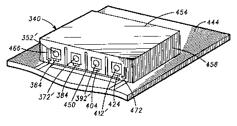
Turning next to FIG. 5, filter circuit 340 shown in the electrical
schematic representation of FIG. 4 is shown in perspective, here
mounted upon electrical circuit board 444.
The ceramic block forming a portion of filter circuit 340
5 illustrates, in the view of FIG. 5, top face surface 450 and side
surfaces 454 and 458. (Additional side surfaces of the ceramic block
are hidden from view in the figure.) Openings defined by
trs~n~mi~.~ion lines 352', 372', 392', and 412' are formed at top surface
450. Variable capacitors, here varactors or voltage variable
capacitors, 364, 384, 404, and 424 are also formed upon top surface
450. The variable capacitors 364,384, 404, and 424 are positioned in
manners analogous to the positioning of variable capacitor 264 of
filter circuit 240 of FIGS. 2 and 3. Additionally formed on top surface
450 are couplers 466 and 472. Couplers 466 and 472 correspond to
15 coupling ports formed at opposing ends of filter circuit 340 shown in
the electrical schematic representation of FIG. 4.
The ceramic block comprising a portion of filter circuit 340 is
mounted upon circuit board 444 in conventional manner to connect
couplers 466 and 472 to circuit paths disposed upon circuit board 444.
20 In a simil~r manner, circuit paths may be formed to extend to
variable capacitors 364, 384, 404, and 424 to apply control signals to
control the capacitive values of such variable capacitors.
As mentioned previously, particularly with respect to the block
diagram of FIG. 1, the tunable filter circuits of the preferred
25 embodiments of the present invention may be advantageously utilized
to form a portion of a cellular radiotelephone operative in a TDMA
communication scheme. In such an application, the center
frequency of the filter circuit must be of a first center frequency (and
of a first bandwidth) when the radiotelephone is operative to receive
30 modulated sign~l~ and must be of a second center frequency (and of a
second bandwidth) when the radiotelephone is operative to transmit
modulated signals. For instance, when transmitting modulated
signals, the filter must be of a center frequency of, for example, 897.5
MHz, and when the radiotelephone is operative to receive modulated
3~ signals, the center frequency of the filter must be of a frequency of
WO 94127376 PCT/US94/04363
'2,~3~033 - 16 -
942.5 MHz. As frequency is inversely related to the square root of
capacitance, a capacitive ratio, CR, is determined by the following
equation:
CR = Cmax/Cmin = (~min)2/(Fmàx)2
wherein:
CmaX= the equivalent capacitance for the first, maximum
center frequency;
Cmin is the equivalent capacitance required of the second,
minimum center frequency;
FmaX is the first, maximum center frequency; and
Fm,n is the second, minimum center frequency.
In the example just-shown, the capacitive ratio is 1.103 (i.e.,
(942.5/897.5)2 = 1.103). Hence, if the equivalent capacitance required of
the filter circuit when the center frequency is to be 942 MHz is 2 pF,
the equivalent capacitance required of the filter circuit when the
center frequency is to be of 897 MHz is of a value of 2.206 pF. Control
si~n~l~ applied to the various variable capacitors of the tunable filter
must permit such equivalent capacitances to be formed.
Finally turning now to the logical flow diagram of FIG. 6, the
method steps of the method, referred to generally by reference
numeral 800, of a preferred embodiment of the present invention are
listed. Method 600 constructs a filter of a block of dielectric material
defining top, bottom, and at least first and second side surfaces.
First, and as indicated by block 806, at least one longitudinally-
extending resonator is formed between the top and bottom surfaces of
the dielectric block.
Next, and as indicated by block 812, at least a portion of the
bottom and first and second side surfaces of the dielectric block are
covered with a coating of an electrically-conductive material.
And, as indicated by block 818, at least one variable capacitor is
coupled in an electrical connection with the at least one resonator
wherein the variable capacitor is variable to be of at least either a first
capacitive value or a second capacitive value.
WO 94/27376 PCT/US94/04363
2138033
While the present invention has been described in
connection with the preferred embodiments shown in the various
figures, it is to be understood that other similar embodiments may be
used and modifications and additions may be made to the described
5 embodiments for performing the same function of the present
invention without deviating therefrom. Therefore, the present
invention should not be limited to any single embodiment, but rather
construed in breadth and scope in accordance with the recitation of
the appended claims.
t ~
J~ i Q,--.Y