Note: Descriptions are shown in the official language in which they were submitted.
WO 93/25984 PCT/US93/05503
- 1 -
TITLE
METHOD AND APPARATUS FOR THEFT DETECTION USING DIGITAL
SIGNAL PROCESSING
BACKGROUND OF THE INVENTION
Field of the Invention
This invention relates to the processing of electrical
signals and in particular it concerns novel methods and
apparatus for utilizing digital signal processing in
electronic theft detection.
Description of the Prior Art
United States Patent No. 4,623,877 to Pierre F. Buckens
and assigned to the assignee of the present invention
discloses and claims methods and apparatus for
detecting the unauthorized taking of objects from a
protected area, such as a store. Articles taken from
the store must pass through an interrogation zone into
- which electromagnetic interrogation energy is
continuously radiated. If, while an article is brought
. 25 through the interrogation zone, it has an active target
w mounted thereon, the target will respond to the
' electromagnetic interrogation energy in the zone and
WO 93/25984 PCT/US93/05503
- 2 -
will produce disturbances of that energy in the form of
pulses having unique characteristics. These pulses are
detected by a receiver at the. interrogation zone.
The Buckens invention makes use of signal processing to
ascertain the average signal level in the interrogation
zone at different portions of each interrogation cycle
and to adjust the detection threshold level according
to that level so that targets may be detected in the
presence of other objects which may also produce
interfering signals.
SUN~IARY OF THE INVENTION
The present invention provides additional improvements
to those of the Buckens invention. More specifically,
the present invention, in one aspect, completely
eliminates, in a novel manner, the effects of
electromagnetic energy which is not synchronously
related to signals which are to be detected. In
another aspect, the invention makes target responses in
an electronic article surveillance system more
detectable by means of signal processing which
substantially eliminates selected frequency components
from energy to be detected and then replaces the
original phase relationships among the remaining
components, thereby preserving the unique
characteristics of signals produced by the special
targets attached to articles to be protected.
The present invention in one aspect involves novel
methods and apparatus for processing signals of known
periodicity by controlling their flow according to the
amplitude variation among samples taken in
correspondiwg time intervals in each of plural signal
periods.
WO 93/25984 PCT/US93/05503
- 3 -
According to another aspect of the present invention
there are provided novel methods and apparatus for
detecting the presence, in an interrogation zone, of a
target capable of producing predetermined
electromagnetic disturbances which repeat at a first
predetermined frequency and which have distinctive
characteristics defined by frequency components in a
frequency band principally less than a second, higher,
predetermined frequency. These methods and apparatus
comprise the steps of and apparatus for receiving
electromagnetic disturbances from the interrogation
zone and producing corresponding electrical s°,~nals,
removing or filtering from the electrical signals,
frequency components above a third frecr~.~Ancy higher
than the second frequency, detecting t=.~ :aagnitude of
the remaining portions of the electrica~_ signals during
successive time intervals at a frequency at least t~..-a
the third frequency and which frequency is also a
multiple of the first predetermined frequency, then
comparing the detected magnitudes which occur in
corresponding time intervals in successive cycles of
the first predetermined frequency and producing an
alarm signal in response to a predetermined comparison
result.
According to further~aspects of the invention there are
provided other novel methods and apparatus for
detecting the presence, in an interrogation zone, of a
target capable of producing predetermined
electromagnetic disturbances which repeat at a firs.r_
predetermined frequency. These other n::;-.rel methods ~.nd
apparatus comprise the steps of and apparatus for
receiving electromagnetic disturbances from the
interrogation zone and for producing corresponding
electrical. signals,~detecting the magnitude of the
electrical signals during successive time intervals,
which time intervals occur at a second frequency which
WO 93/25984 PCT/US93/05503
is a predetermined multiple of the first predetermined
frequency, comparing the detected magnitudes of the
electrical signals which occur in corresponding time .
intervals in successive cycles of~the first
predetermined frequency to produce an alarm, and
preventing the production of an alarm in those time
intervals where the variation among the compared
magnitudes fails to conform to a predetermined
characteristic.
According to additional aspects of the invention there
are provided further novel methods and arrangements for
detecting the presence of a target in an interrogation
zone. These further novel methods and apparatus
comprise the steps of and apparatus for, detecting the
electromagnetic radiation in the interrogation zone and
producing electrical signals corresponding to the
radiation, filtering from the electrical signals
selected frequency components, restoring to the
remaining components the relative phase relationship
the remaining components had to each other prior to
filtering, and detecting the presence of predetermined
pulses in the restored components.
According to still further aspects of the invention
there are provided novel methods and arrangements for
augmenting, by predetermined amounts, the magnitude of
signals from taps which are distributed along a signal
delay circuit wherein the signals, after being so
augmented, are connected to a common summing circuit.
These other novel methods and arrangements comprise
steps and apparatus for producing a difference signal
representing the difference in magnitudes between the
output of the summing circuit and a desired magnitude,
w 35 multiplying the magnitude of a signal corresponding to
the.difference signal with each of the signals at the
output of the delay line to produce individual
WO 93/25984 PC?/US93/05503
- 5 -
adjustment signals, adding to these adjustment signals
to previously produced tap coefficients to produce new
tap coefficients, delaying the new tap coefficients and
amplifying each tap output by an amount corresponding
to its respective delayed new tap coefficient.
BRIEF DESCRIPTION OF THE DRAWINGS
Fig. 1 is a perspective view of an electronic theft
detection system embodying the present invention as
installed in a supermarket;
Fig. 2 is a diagrammatic view of the general components
of the system of Fig. 1;
Fig. 3 is a block diagram of the components of the
system of Fig. 1;
Fig. 4 is a series of waveforms showing the relative
timing of signal processing in the system of Fig. 1;
Fig. 5 is a further block diagram of a noise blanker
portion of the system of Fig . 4 ;
Fig. 6 is a block diagram of long and short term
averagers used in the system of Fig. 1; and
Fig. 7 is a further block diagram of a pulse
straightener portion of the system of Fig. 3.
DETAILED DESCRIPTION OF THE PREFERRED EMBODIMENT
The present invention is applicable to any electronic
article surveillance system in which a target causes
rapid periodic electromagnetic disturbances. However;
for purposes of illustration the invention will be
described in conjunction with a so-called "magnetic"
WO 93/25984 PCT/LJS93/05503
- 6 -
system in which an alternating magnetic field is
introduced into an interrogation zone and targets on
protected articles carried_tlirough the zone are driven
alternately into and ou~~~of magnetic saturation by the
alternating magnetic field. This produces periodic .
electromagnetic disturbances at frequencies which are
harmonics of the original alternating magnetic field
frequency. These harmonics, or selected ones of these
harmonics, are detected and used to actuate an alarm.
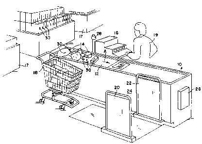
The arrangement shown in Fig. 1 is used in a
supermarket to protect against theft of merchandise.
As shown, there is provided~a supermarket checkout
counter 10 having a conveyor belt 12 which carries
merchandise, such as items 14 to be purchased, past a
cash register 16, as indicated by an arrow A. A patron
(not shown) who has selected goods from various shelves
or bins 17 in the supermarket, takes them from a
shopping cart 18 and places them on the conveyor belt
12 at one end of the counter 10. A clerk 19, standing
at the cash register 16, records the price of each item
of merchandise as it moves past on the conveyor belt.
The items are paid for and are bagged at the other end
of the counter. The theft detection system according
to this embodiment of the invention may include a pair
of spaced apart antenna panels 20 and 22 next to the
counter 10 beyond the cash register 16. The antenna
panels 20 and 22 are spaced far enough apart to permit
the store patron and the shopping cart to pass between
them.
The antenna panels 20 and 22 contain transmitter
antennas which are simply loops or coils of wire or
other conductive material capable of generating
magnetic fields when electrical currents pass through
them. These antennas generate an alternating magnetic
field in an interrogation zone 24 between the panels.
WO 93/25984 PCT/US93/05503
".
The antenna panels 20 and 22 also contain receiver
antennas, which are also conductive coils capable of
converting incident electromagnetic energy to
electrical currents. These receiver antennas thus
produce electrical signals corresponding to variations
in the magnetic interrogation field in the zone 24.
The antennas are electrically connected to transmitter
and receiver circuits contained in a housing 26
arranged on or near the counter 10. There is also
provided an alarm, such as a light 28, mc.unted on the
counter 10, which can easily be seen by the clerk and
which is activated by the electrical circuit when a
. protected item 14 is carried between the antenna panels
and 22. If desired, an audible alarm may be
15 provided instead of, or in addition to, the light 28.
Those of the items 14 which are to be protected against
shoplifting are provided with targets 30. Each target
comprises a thin elongated strip of high
20 permeability easily saturable magnetic material, such
as permalloy. When protected items 14 are placed on
the conveyor belt 12 they pass in front of the clerk 19
who may record their purchase. The items 14 which pass
along the counter 10 do not enter the interrogation
25 zone 24 and they may be taken from the store without
sounding an alarm. However, any items which remain in
the shopping cart 18, or which are carried by the
patron cannot be taken from the store without passing
between the antenna panels 20 and 22 and through the
30 interrogation zone 24. When an item 14 having a target
30 mounted thereon enters the interrogation zone 24, it
becomes exposed to the alternating magnetic
interrogation field in the zone and becomes magnetized
alternately in opposite directions and driven
repetitively into and out of magnetic saturation. As a
result, the target 30 disturbs the magnetic field in
the interrogation zone in a manner such that pulses of
WO 93/25984 ~ ~ PCT/US93/05503
_ g _
magnetic energy are formed. These pulses, which are
made up of frequency components at harmonics of the
original or fundamental transmitted frequency, have a .
unique form, which makes it possible to detect their
occurrence. The magnetic fields in the interrogation
zone, including those which form the above described
pulses, are intercepted by the receiver antenna which
produces corresponding electrical signals. These
electrical signals, as well as other internally
generated electrical signals, are processed in the
receiver circuits in a manner such that those produced
by true targets can be distinguished from those
produced by other electromagnetic disturbances and
other internally generated electrical signals. Upon
completion of such processing, the signals produced by
true targets are then used to operate the alarm light
28. Thus the clerk 19 will be informed whenever a
patron may attempt to carry~unpurchased protected
articles out of the store.
Fig. 2 is a diagrammatic representation of the system
of Fig. 1 as seen from a position along the path of
movement through the interrogation zone 24. As
indicated, transmitter circuits 40 are connected to a
transmitter antenna 42 on one side of the interrogation
zone 24; and a receiver antenna 44 on the other side of
the zone 24 is connected to receiver circuits 46.
These receiver circuits in turn are connected to an
alarm 48. It has been found preferable to provide
transmitter and receiver antennas on both sides of the
zone 24; but for purposes of illustration and
explanation Fig 2 shows a single transmitter antenna on
one side and a single receiver antenna on the other
side.
'
The transmitter circuits 40 generate a continuous
alternating electrical signal in the form of a sine
WO 93/25984 ~ ~r ~ ~ PCT/US93/05503
_ g _
wave and at a fixed fundamental frequency, for example,
218 HZ. This electrical signal is converted by the
transmitter antenna 42 into a corresponding alternating
magnetic interrogation field in the interrogation zone
24. The transmitted interrogation field is represented
by the waveform I near the transmitter antenna 42. As
can be seen, this waveform is in the shape of a sine
wave. A target 30 in the interrogation zone 24
disturbs the field transmitted by the transm~~ter
antenna and produces small pulses P as shown in a
waveform II near the receiver antenna. The waveform II
is basically the same shape as the waveform I except
that the waveform II is slightly displaced in time due
to its transit time across the interrogation zone.
Further, the waveform II has pulses superimposed
thereon which are caused by the target 30 in the zone.
It should be noted that the waveform II, which has the
same fundamental frequency as the waveform I, is
synchronized with the wave form I. In addition, the
pulses P in the wave form II are also synchronized with
the waveform I. These pulses are actually the sum of
several frequency components which are harmonics of the
fundamental frequency of the transmitted magnetic
field.
The receiver antenna 44 converts magnetic fields which
are incident thereon, including the waveform II, to
corresponding electrical signals. These electrical
signals are processed in the receiver circuits 45 to
ascertain whether the magnetic field disturbances are
those which have been caused by the pres:.ce. of a true
target 30 in the interrogation zone 24. If so, the
receiver circuits send a signal to actuate the alarm
circuit 48.
It should be understood that in addition to the
magnetic field from the target 30 which produces the
WO 93/25984 PCT/US93/05503
_ _
N lO
waveform II, there are several other magnetic fields
incident on the receiver antenna 44. These other
fields may be caused by spurious electromagnetic
disturbances from electrical equipment such as motors,
lights, radio transmission, etc., or even by "innocent"
objects, such as shopping carts or other metallic
objects which disturb the magnetic field produced by
the transmitter antenna 42. In addition, internally
generated electrical disturbances alter the electrical
signals produced by the receiver antenna 44. The
system described herein uses various signal processing
techniques to distinguish those disturbances produced
by the presence of a true target 30 in the
interrogation zone from the above mentioned other
disturbances. Some of these techniques have been used
in the past. The novel features of the present
invention provide improvements over these past
techniques in the following respects: first, the
present invention makes it possible to remove, rather
than merely attenuate the effects of electrical and
electromagnetic disturbances which are not synchronous .
with the transmitted magnetic field; and second, the
present invention makes it possible to process the
received electromagnetic signals without significant
phase or delay distortion due to filtering so as to
maintain the characteristic shapes of the received
signals. These features will become apparent from the
following description of the internal configuration of
the transmitter and receiver circuits.
The overall block diagram of the transmitter and
receiver circuits 40 and 46 is shown in Fig. 3. A
clock generator 50 and a divider 52 are provided to
synchronize the overall operation of the system. In
this example the clock generator is chosen to produce
pulses at a rate of 13,952 pulses pe,r second on a
sample clock signal line 51. The divider 52 is
WO 93/25984 PCT/US93/05503
21~~~~~
- 11 -
connected to the sample clock signal line 51 and is
constructed to produce one output pulse for every 64
input pulses, that is, 218 pulses per second on a cycle
clock signal line 53. The pulses from the divider 52
are applied to a low pass filter 54 which converts them
to a continuous sine wave of 218 HZ. This sine wave is
applied to an amplifier 56 which is connected to drive
the transmitter antenna 42. The transmitter antenna 42
thus generates a continuous alternating magnetic field
in the interrogation zone 24 as indicated by the
waveform I in Fig. 2. The clock pulse generator 50,
the divider 52, the low pass filter 54 and the
amplifier 56 are all individually well known and no
special form of any of these omponents is needed or
desired in order to carry out the invention according
to the best mode contemplated by the inventors.
Electromagnetic energy from the interrogation zone 24,
including disturbances produced by a target 30, if
present, as well as other electromagnetic disturbances
that may be present, are received by the receiver
antenna 44 and converted to corresponding electrical
signals. These signals are applied to front end
amplifier and filter circuits 60. These front end
circuits are designed to remove or reduce unwanted
components from the electrical signals generated by the
receiver antenna 44, particularly the very large
fundamental frequency of the transmitter signal (i.e.
218 HZ). The front end circuits 60 are also
individually well known and no special form is needed
to carry out the invention. As mentioned, the front
end amplifier and filter circuits 60 remove or reduce
the very large fundamental frequency component, i.e.
the 218 HZ component. For this purpose a notch filter
has been found to be the simplest and most effective
way to reduce this component.
WO 93/25984 ~ PCT/US93/05503
- 12 -
The front end amplifier and filter circuits 60 are
connected through a first training/nozmal operation
switch 61 (to be described~more fully hereinafter) to
internal amplifier and band-pass filter circuits 62.
The purpose of these circuits is to attenuate frequency
components above and below a predetermined frequency
band. It has been found that those frequency
components below the tenth and above the seventeenth
harmonic of the fundamental frequency can be attenuated
and the remaining components will closely represent the
major distinctive features of the target produced
pulses. Also, by attenuating the components above the
seventeenth and below the tenth harmonic, a large
portion of the interfering electrical energy from non-
target sources is removed.
The internal amplifier and band-pass filter circuits 62
are also well known and no special construction thereof
is considered to be the best mode for carrying out this
invention. In the illustrated embodiment the filter
portion of the internal amplifier and band-pass filter
circuits 62 is made up of a 9th order Butterworth
highpass filter with a cutoff frequency of 2 KHZ
(kilohertz) and a 9th order 0.01 db (decibel) Chebyshev
lowpass filter with 3db down or -3db at 3800 HZ cutoff.
The output of the internal amplifier and band-pass
filter circuits 62 is connected to an analog to digital
converter 64 which produces a digital output
corresponding to the amplitude of the signal from the
circuits 62 at any instant.
The output from the analog to digital converter 64 is
applied to each of M processors 65. Each processor
comprises noise blanker circuits 67 and long and short
term averager circuits 68. .The output of each
processor 65 is applied to a corresponding input
70a,...70aM of a sample demultiplexer 70; and the single
WO 93/25984 PCT/US93/05503
- 13 -
output of the sample demultiplexer 70 is applied to an
adaptive equalizer 72.
In the illustrative embodiment, which is presently
preferred the number M is chosen to be sixty-four,
which accommodates sixty-four samples during each cycle
of the fundamental frequency. The amplifiers and
filters 60 and 62 are designed to pass the 10th through
17th harmonics of the fundamental frequency and to
attenuate frequency components above and below this
band. Because of the characteristics of the filters,
.frequency components up to the 32nd harmonic may be
passed to some appreciable degree. Therefore, to
ensure against aliasing, the sampling and processing by
the M processors 65 is at a rate substantially in
excess of twice that frequency, namely, the 64th
harmonic.
The output of the adaptive equalizer 72 is applied
through a full wave rectifier 73 to a signal channel
74, which contains a signal gate 76 and a low pass
filter 78, and a noise channel 80, which contains a
noise gate 82 and a peak detector 84. The outputs of
the signal and noise channels 74 and 80 are compared in
a comparator 86; and the comparator output is applied
to the alarm 48. The signal and noise gates 76 and 82
are opened to pass signals along their respective
signal and noise channels 74 and 80 at alternate times
by gate signals from a gate generator circuit 88. The
gate generator circuit 88 in turn receives pulses from
the divider 52.
The portion of the system following the adaptive
equalizer 72, namely the portion containing the full
.w ~35 wave rectifier 73 and the signal and noise channels 74
and 80 is, in principle, the same as described in the
above referred to United States Patent No. 4,623,877 to
WO 93/25984 PCT/US93/05503
- 14 -
Pierre F. Buckens, except that it is preferably
implemented using well known digital circuits.
Here it should be understood that while the processors
65, the sample demultiplexer 70, the adaptive equalizer
72 and the remaining components are all shown and
described herein using block diagrams, the functions of
these items in actual practice would be carried out by
means of solid state integrated circuit components
formed on chips that have been specially programmed to
perform the functions to be described. It should also
be understood the actual manner of programming the
integrated circuit components is not part of the
invention nor does it concern the best mode of carrying
out the invention. Any programmer of ordinary skill in
the art can program solid state components to perform
the functions to be described; and there are many
different ways of carrying out this programming, with
no particular one being considered to be better than
any other.
The first training/normal operation switch 61 has a
first input terminal 61a which is connected to the
output of the front end amplifier and filter circuits
60, a second input terminal 61b which is connected to
the output of a test pulse generator 63 and a common
output terminal 61c which is connected to.the input of
the amplifier and bandpass circuits 62. The switch 61
is controlled by a programmed training/normal operation
control unit 151, which also controls a second
training/normal operation switch to be described
hereinafter in connection with the adaptive equalizer
72. As shown, the adaptive equalizer 72 is also
connected to receive signals from the training/normal
operation switch control unit 151. Thus, depending on
the setting of the first training/operation switch 61,
signals are directed to the amplifier and bandpass
WO 93/25984 ~ ~ ~ ~ ~ PCT/US93/05503
- 15 -
filters 62 either from the receiver antenna 46 and
front end circuits 60 or from the test pulse generator
63.
The test pulse generator 63 is connected to receive
cycle clock signals from the output of the divider 52
and to produce from each of these pulses a pulse
similar to that which would come from the front end
circuits when a true target 30 is present in the
interrogation zone. During a "training" period, prior
. to normal operation of the system, ~:_he
training/operation switch 61 is set with its second
input terminal 61b connected to its common output
terminal 61c and the pulse signals from the test pulse
generator 63 are at this time applied to the amplifier
and band pass circuits 62. During normal operation of
the system, the switch 61 is set with its first input
terminal 61a connected to the common output terminal
61c, so that signals from the receiver antenna 46 and
the front end circuits 60 are applied to the amplifier
and band pass circuits 62.
Before describing the sample clock multiplexer 66, the
noise blanker circuits 67, the averager circuits 68,
the sample demultiplexer 70 and the adaptive equalizer
72, the general manner in which the system analyzes
incoming signals will first be described in connection
with Fig. 4. Waveform (a) of Fig. 4 represents the
magnitude of the transmitted magnetic interrogation
field which alternates at the fundamental frequency,
which is the illustrative embodiment is 218 HZ.
Waveform (b) of Fig. 4 represents the magnitude of an
idealized signal incident on the receiver antenna 44
when a target 30 is present in the interrogation zone
3.5 24. As can be seen, the signal is dominated by the
waveform of the alternating magnetic. interrogation
field from the transmitter antenna 42. This
WO 93/25984 PCT/US93/05503
_ _ .,..
16
alternating magnetic field is at the transmitter or
fundamental frequency of 218 HZ: The presence of the
target 30 in the interrogation zone causes slight .
disturbances (P) of the magnetic field as a result of
the target 30 being driven into and out of magnetic
saturation twice during each cycle. A large portion of
the signal produced by this alternating magnetic field
at the fundamental frequency (218 HZ) is eliminated by
the notch filter in the front end amplifier and filters
60. However, some remaining portion of this signal
component is still present. The internal amplifier and
band-pass filters 62 further attenuate the remaining
portions of the fundamental frequency component as well
as other components below the 10th harmonic and above
the 17th harmonic of the fundamental frequency. Thus
the output of the internal amplifier and band-pass
filters 62 is made up of those frequency components
which they pass, namely those components between 2,180
HZ and 3,706 HZ. While this is only a portion of the
total spectrum of the frequency components of the
pulses produced by the target 30, it has been found
that this portion of the spectrum contains a sufficient
amount of the components peculiar to the target 30.
Accordingly the portion of the frequency spectrum
between the 10th and the 17th harmonics of the
fundamental frequency is well suited for accurate
target discrimination.
The waveform (c) of Fig. 4 is an idealized
representation of true target pulses with the frequency
components below the 10th and above the 17th harmonics
removed. However, the actual form of the pulses is
more like that shown in the waveform (d) of Fig. 4.
This is because the filtering produced by the circuits
60 and '62 causes the retained frequency components to
become phase shifted with respect to each other. Thus,
the resulting pulses are spread out in time. In one
WO 93/25984 PCT/US93/05503
~~~~c~1
- 17 -
aspect of the invention this pulse spreading effect is
compensated so that several closely spaced pulses can
be separately analyzed.
In carrying out the present invention, the signals from
the internal amplifier and bandpass circuits 62 are
sampled at several instances during each transmitter
cycle. It will be recognized that the more samples
that are taken during each transmitter cycle, the
closer the samples will follow the actual pulses
resulting from the disturbances produced by the target
30. It has been found however that as long as the
samples are taken at a rate which is greater than twice
the frequency of the highest harmonic carried in the
sample, the resulting sample composite will contain
sufficient information to reproduce the pulses without
any aliasing effects. In consideration of attenuation
characteristics of the circuits 60 and 62, particularly
the low pass filtering produced in the circuit 62, and
in consideration of the resolution of the analog to
digital converter 64 (e. g. twelve bits), a sampling
rate of 64 times the fundamental frequency of 218 HZ is
considered sufficient to avoid, for all practical
purposes, the effects of aliasing.
Thus the signals produced by the target 30 occur at a
first frequency, namely, twice the fundamental
frequency of the transmitter, which in this embodiment
is 218 HZ. The frequency components which are used to
ascertain the distinctive characteristics of the target
signals extend up to a second, higher, frequency, which
in this illustrative embodiment is the 17th harmonic,
namely 3,706 HZ. The attenuation provided by the
filters in the system effectively eliminate, or at
least reduce to below an appreciable level, all
frequency components below a third, still higher
frequency, which in this illustrative embodiment, is
WO 93/25984 PCT/US93/05503
~1
- la -
the 32nd harmonic, namely 6,976 HZ. To avoid aliasing,
samples are taken at a frequency of at least twice the
third frequency, namely, the 64th harmonic or 13,952
HZ.
As indicated in Fig. 3, there are provided as many
noise blanker circuits 67 and signal averager circuits
68 as there are samples to be taken during each cycle;
and each of these circuits is assigned to a
corresponding sample interval. Thus, the sample clock
multiplexer 66 has a single input terminal 66a at which
,the sample clock signal from the clock generator 50 is
applied, and 64 outputs 66b,...66bM each connected to a
corresponding one of the noise blankers 67 and averager
circuits 68. Thus the multiplexer 66 switches the
clock signal on its common input terminal 66a to each
of its output terminals 66b,...66bM at a rate of 13,952
times per second or 64 time during each cycle of the
fundamental interrogation frequency (218 HZ). Since an
integral number (M) samples are taken during each cycle
of the interrogation field and since the switching of
the sample multiplexer 66 repeats after every M
samples, and since each sample from the analog to
digital converter 64 is made available to the noise
blanker 67 in each of the M processors 65, each of the
noise blankers 67 and signal averagers 68 operate on
the sample associated with only an associated one of
the M corresponding portions of successive magnetic
field interrogation cycles.
In one aspect, the present invention eliminates signals
which do not have a sufficient degree of consistency
from cycle to cycle of the interrogation field. When a
true target 30 passes through the interrogation zone 24
it.produces pulses in corresponding portions.of each
interrogation field cycle. Since the interrogation
field cycle is 218-' seconds (0.0046 seconds), a true
WO 93/25984 ~ "~ ~ PCT/US93/05503
- 19 -
target, whose passage time when carried through the
interrogation zone is about 1.5 seconds, would ideally
experience about 326 interrogation cycles and may
produce about that many pulses. Actually, magnetic
nulls are encountered along most paths so that less
than 326 interrogation cycles are capable of producing
target responses. It has been found that if only three
pulses occur in a sequence of three successive
interrogation cycles and if those pulses all have quite
similar amplitude, it is likely that they were produced
by a true target passing through the interrogation zone
and not by a passing spurious electromagnetic
disturbance or by some other energy source which is not
synchronous with the magnetic interrogation field.
However, a greater number of pulses from a
correspondingly greater number of cycles may be
compared to provide an even finer degree of
selectivity.
The processing of several signal samples from
corresponding parts of several successive interrogation
cycles to ascertain the presence of a true target is
not new. What is new, among other things, is the fact
that in this invention, the successive samples are not
processed in a manner which merely gives a weighted sum
of those signals. Instead in the present invention the
successive samples are compared in a manner which takes
into account their deviation from each other. In other
words, the consistency of sample amplitude from cycle
to cycle is used as a criterion to ascertain whether
the signals are being produced by an object which has
been energized by the transmitter as opposed to one
whose exitation originated from an outside source not
associated with the system. When only an arithmetic
3.5 average . is used, a very large spike in one cycle may be
sufficient to raise the signal level for several cycles
by an amount to indicate the presence of a target, even
WO 93/25984 PCT/US93/05503
- 20 -
though a target may not be present. However if the
deviation from cycle to cycle is taken into account
then the very large spike. can be discounted.
As specifically carried out, the present invention, in
one aspect, processes the amplitudes of the samples
taken at corresponding portions of N successive signal
samples (for example, N=3 cycles), to ascertain whether
the square of the sum of the sample amplitudes is
greater than a predetermined constant K,~, (threshold
constant), multiplied first by the same number of
cycles, and multiplied further by the sum of the
squares of the sample amplitudes. Typically, the
constant K,,, has a value between 0 and 1 and may be
supplied to the system in a manner which renders it
field-adjustable. If the square of the sum of the
sample amplitudes is greater, the system will allow the
latest signal sample amplitude to pass through to the
averagers for further processing, and at the same time
will hold the value of the sample for comparison in the
same manner with sample amplitudes which will be taken
from corresponding portions of subsequent interrogation
cycles. If the square of the sum of the sample
amplitudes is less than the latter value, the system
will not allow the sample amplitude to pass through to
the averagers but it will hold the sample value for
comparison in the same manner with sample amplitudes
which will be taken from corresponding portions of
subsequent interrogation cycles. Instead, it will feed
back to the averagers the output of the long term
averager for the selected sample interval.
The noise blanker block diagram of Fig. 5 shows the
construction of the noise blanker 67 which makes the
above described comparisons. As can be seen in Fig.~S,
there is provided, for each of the noise blanker
circuits 67, a summer 90 which, at one input terminal
PCT/US93/05503
WO 93/25984
- 21 -
90a, receives inputs from the analog to digital
converter 64. The summer 90 also receives, at a second
input terminal 90b, negative values of long term
averages signals. The significance of these last
mentioned long term averages signals will be described
hereinafter. The summer 90 supplies its outputs to
storage elements 94" 94z, 943 (up to N such elements).
Each element is activated by an output of the cycle
clock multiplexes 92. The output of the sample clock
multiplexes is connected to a common input terminal 92a
of a cycle clock multiplexes 92. The cycle clock
multiplexes 92 uses signals from the cycle clock signal
line 53 to switch its sample clock multiplexes signal
input terminal 92a to each of its output terminals
92b,...92bN in succession, although, as mentioned above,
sample amplitudes from only three successive cycles are
taken in the present embodiment to obtain an indication
as to whether any of them were produced by spurious or
non synchronous energy. Therefore the cycle clock
multiplexes 92 has three output terminals 92b" 92b2 and
92b3. For certain applications it may be desired to
provide a finer resolution of the distinction between
spurious or non synchronous energy and synchronous
energy. In such case a larger number N of output
terminals up to 92bN from the cycle clock multiplexes
may be provided along with the associated additional
elements shown connected by dashed lines.
It should be understood that the cycle clock
multiplexes 92, like the sample multiplexes 66,
recycles, so that the next cycle clock transition to
occur after the multiplexes has been switched to its
last output terminal, causes the multiplexes to be
switched again to its first output terminal.
~3 5
WO 93/25984 PCT/US93/05503
- 22 -
The output terminals 92b,..,.~92bN of the cycle clock
multiplexer 92 are con-netted to associated signal
storage devices 94~, ,942, 943...94N. The storage devices
are capable of holding the value of the sample last
applied to their input terminal 9418, 942x, 943a...94"a. .
This signal value appears continuously at the
respective storage device's output terminal 941b, 942b~
943b, 94nb~ However, when the storage device's input
terminals 941, 9428, 943a ~ ~ ~ 94N, become active, the old
sample value in the storage device is replaced by the
new value provided by the value at the summer output
terminal 90c.
The sample values in the signal storage devices are
applied continuously to a sample value summer 100 where
they are combined arithmetically. The resulting
arithmetic sum is then applied to a squaring circuit
102 which produces an output corresponding to the
square of its input. The squaring circuit 102 thus
produces an output corresponding to the square of the
sum of the successive sample values. The output of the
squaring circuit 102 is applied to a plus input
terminal 104a of a comparison circuit 104.
The sample values in the signal storage devices 941,
942, 943...94N are also applied to individual squaring
circuits~106, 108, 110, etc. which, respectively,
produce output values corresponding to the square of
the values of the signals applied to their input. The
outputs of the squaring circuits 106, 108, 110, etc.
are applied continuously to a sample squared summer
circuit 112 which produces an output value
corresponding to the arithmetic sum of its inputs. The
output of the sample squared summer 112 is thus a value
corresponding to the sum of. the squares of the values
stored in the storage devices 941, 942, 943...94N.
WO 93/25984 PCT/US93/05503
- 23 -
The output of the sample squared summer 112 is applied
to a multiplier circuit 114 where its value is
multiplied by a number N, corresponding to the number
of signal storage devices (in this embodiment, three),
and by a preset value KY1" which represents the
threshold of signal value consistency needed to prevent
a pulse from passing to the averagers. Typically, K;1,
varies from 0 to 1. The output of the multiplier
circuit 114 is applied to a negative input terminal
104b of the comparator circuit 104.
.The comparator circuit 104 is applied to a switch
actuation terminal 116a of an inhibit switch 116. The
inhibit switch 116 has a first signal input terminal
116b which is connected to rec:~ ve the same signals
which are applied from the analog to digital converter
64 to the input terminal 90a of the summer 90. The
inhibit switch 116 also has a second signal input
terminal 116c which is connected to receive signa~s
from a long term averager to be described. When the
output of the comparator circuit is more positive than
negative, that is, when the square of the sums in the
storage devices 941, 94z, 943...94N is greater than the
sum of the squares of those signals times N times K,1"
its output causes a common terminal 116d of the switch
115 to be connected to its first signal input terminal
116b so that the common terminal 116d receives signals
directly from the analog to digital converter 64.
However, when the output of the comparator circuit is
more.negative than positive, its output causes the
common terminal 116d of the switch 116 to be connected
to its second signal input terminall 116c so that its
common terminal receives signals only from the long
term averager (to be described).
The signals from the analog to digital converter 64
which are applied to the noise blankers 67 are
WO 93/25984 PCT/US93/05503
- 24 -
composite signals which include a first component of
known periodicity, namely, the.period separating
alternate target produced 'responses, and a second .
component not of the known periodicity, namely, that
resulting from other sources. The noise blankers
compare the amplitudes of the composite signals from
corresponding time intervals in each of a plurality of
signal periods and operate their respective switches
116 to control the flow of the composite signals to
further processing circuits, namely, the signal
averagers 118 and 120, according to the degree of
variation in those amplitudes. The components of known
periodicity are closely similar to each other in
amplitude from cycle to cycle; and if they predominate,
the noise blanker will move the switch 116 to its upper
position to pass the composite signal to the further
processing circuits. If, however, the components which
are not of'the known periodicity predominate, they will
not be similar in amplitude from cycle to cycle and the
noise blanker will move the switch 166 to its lower
position so that the composite signals will not pass to
the averager circuits 118 and 120.
The common terminal 116d of the switch 116 in the noise
blanker circuit 67 is connected, as shown in Fig. 6, to
both a short term averager 118 and a long term averager
120. The short term averager 118 includes a first
multiplier 122, a summer 124, a delay register 126 and
a second multiplier 128. The first multiplier 122 is
connected to receive signals passed by the noise
blanker circuit via the common switch terminal 116d and
to multiply them by a preset value (1-As). The output
of the first multiplier 122 is applied to the summer
124 which adds it to a value from the second multiplier
~5 128. The sum of these values is applied to an input
terminal 126a of the delay register 126 which stores
them and maintains the summed value at an output
WO 93/25984 PCT/US93/05503
- 25 -
terminal 126b until it receives a pulse from the sample
clock multiplexer terminal 66b, which is dedicated to
it. Because of the sample clock multiplexer logic,
each output is activated for only one sample interval
per cycle. Each averager is thus dedicated to a
specific one of M sample intervals and is updated only
during that one interval in each cycle. The output
from the delay register 126 is applied to the second
multiplier 128 where it is multiplied by a preset value
(As). The multiplied value is then applied to the
summer 124.
In operation of the short term averager 118, signal
values applied to the first multiplier 122 from the
noise blanker circuit 67 are multiplied by (1-AS) in the
first multi~.lier 122, summed in the summer 124 with the
output of the second multiplier 128, delayed in the
delay register 126 and multiplied by the value (AS) in
the second multiplier 128. The output is then recycle'
through the summer 124, the delay register 126 and the
second multiplier 128. This produces, at the output of
the delay register 126, an output which is a weighted
sum of the values of the previous input signals from .
the noise blanker circuit 67. The value of the each
previous input signal diminishes in the short term
averager 118 according to the number of times it
circulates through the averager and according to the
value of As. If A were zero then each previous input
signal would go to zero on its first recirculation and
the value of the present input from the noise blanker
circuit would be the new output. This is the shortest
possible averaging. However, as the value of As
increases, the previous input signal values have
greater influence and the averaging period becomes
longer.
WO 93/25984 PCT/US93/05503
~,1
- 26 -
The long term averages 120 is of the same construction
as the short term averages 118, and like the short term
averages, the long term averages 120 comprises a first -
multiplier 130 which receives signals from the noise
blanker circuit 67 and multiplies them by a preset
value, which in this case is designated (1-AL). The
resulting value is added in a summer 132 with an output
value from a second multiplier 134 and the summed value
is applied to a delay register 136. The delayed output
from the delay register 136 is multiplied by a preset
value AL and applied to the summer 132.
The only difference between the long and short term
averagers 118 and 120 is the value of A. The value of
AL in the long term averages 120 is greater than the
value of AS in the short term averages 118 so that the
long term averages takes into account a longer duration
of past signal values in producing an output value. As
mentioned above, the output from the sample clock
multiplexes 66b, which is dedicated to this averages
_ causes the output to be updated over every M sample
interval.
The output of the short term averages 118 is taken from
the output of its delay register 126 and is applied to
a plus input terminal~138a of an averages summing
circuit 138. At the same time, the output of the long
term averages 120 is taken from the output of its delay
register 136 and is applied to a minus input terminal
138b of the averages summing circuit 138. The output
of the averages summing circuit 138 is taken from an
output terminal 138c and is applied to a corresponding
input terminal 70a,...70aM of the sample demultiplexer
70 (Fig. 3). The output of the long term averages 120
is also~applied to the negative input terminal 90b of
the summer 90 in the noise blanking circuit 67
(Fig. 5) .
WO 93/25984 PCT/LJS93/05503
- 27 -
As mentioned above, the noise blanking circuits 67~
operate to prevent passage of any signals unless. the
values of at least three successive pulses applied
thereto have a certain minimum variation. This will
tend to block non-synchronous energy, that is energy
which does not vary in synchronism with the
transmitter. However, there are at times, other non
target energy sources nearby which, for periods of
three or more successive pulses, vary only minimally
but which have a low average value over the period of
the associated short term averager 118. That is, they
do not persist as long as a signal from a target but
while they do occur they may possibly not vary
substantially from pulse to pulse. The signals
produced by these energy sources are attenuated by both
averagers 118 and 120.
The difference of the outputs from the signal averagers
118 and 120 eliminates the effects of unvarying non-
target synchronous energy sources, such as are produced
by metal objects in the range of the transmitted
magnetic fields or are produced internally by the
circuit elements which operate synchronously with the
transmitter. The average value of this unvarying
energy is measured in each long term averager 120 and
is subtracted from the output value of the
corresponding short term averager.118 in the averages
summing circuit 138. Since both averagers contain
identical estimates of these unvarying energy sources,
those signals are cancelled at the output of the
differential summer 138.
The outputs of the long term averagers 120, as
mentioned above,. are applied to the negative input
terminal 90b of the summer 90 in their associated noise
blanking circuits 67. The purpose for this is to keep
the noise blanking circuits sensitive to variations in
WO 93/25984 PCT/US93/05503
- 28 -
the pulse to pulse signal values. If the signal values
of successive pulses vary by a given amount, that
amount will be quite significant if the total signal
value of each pulse is small. But if each pulse is
added to the same large amount, for example from a non
target energy source, then that same variation between
the successive pulses will become relatively less
significant. Therefore, by subtracting from the
incoming pulses, the long term average value of the
energy in the associated sample interval, the pulse to
pulse variation is made more significant.
The outputs from each of the averager summing circuits
138 are combined in the sample demultiplexer 70 (Fig.
3). Each of the averager summing circuit output
terminals 138c are connected to a corresponding input
terminal 70a1...70aM of the demultiplexer 70. The
demultiplexer 70 has a switch actuation terminal 70b
connected to receive pulses from the sample clock
signal line 51. These pulses cause the input terminals
70a~...70aM to be switched, in sequence, to a common
output terminal 71. Thus the signals from the analog to
digital converter, which were divided into time
increments by pulses from the clock generator 50, and
separately processed in the noise blankers and
averagers, are reconstructed in the sample
demultiplexer 70.
By way of further explanation, in the transmitter
portion of the system, the clock generator 50 produces
a signal whose frequency is D*Fo, where D is an integer
and Fo a frequency in hertz. This signal is divided by
the dividers 52 to produce a signal of Fo hertz. The Fo
hertz signal is then further processed, amplified and
applied to the transmitter antenna 42 to create a field
capable of exciting the target~30. The sole
WO 93/25984 PCT/US93/05503
- 29 -
restriction on the method of processing Fo is that the
resulting transmitter field excites the target in such
a manner as to produce a response which is periodic in
Fo.
In the receiver, the receiver antenna 42, which is
capable of sensing the presence of the target 30, is
coupled through a series of filters and amplifiers
which enhance the ratio of target signal energy to non-
target signal energy. The accordingly enhanced output
of these elements is presented to the analog to digital
converter 64. The analog to digital converter
generates sample signals at~ a rate of D*Fo, where the
D*Fo signal is either obtained or derived from the
system transmitter or independently generated in such a
manner that the transmitter and receiver versions are
identical in frequency. It should be noted that there
are no restrictions on the phase relationship between
these signals. The digital conversions of the analog
to digital converter are presented to a functional
block which includes a processor capable of performing
digital signal processing functions at high speeds.
The processor processes the signals applied to it in a
manner which produces a condition representative of the
presence of target, and activates the alarm 48 under
that condition.
The purpose of the noise blanking circuits is to
distinguish between energy which is not a result of the
transmitter's Fo-based signal and which therefore is non
system-synchronous, and that which is system-
synchronous, with a view toward blocking the former
from passing further in the signal processing chain.
It does this by dividing the Fo cycle into D time slots
and making use of the fact that system-synchronous
energy appears repeatedly in the same slot or slots,
WO 93/25984 PCT/US93/05503
- 30 -
while non system-synchronous noise does not and is
randomly spaced in time.
It is important to distinguish between transient
synchronous noise, such as that which occurs when
targets or "innocent" objects are carried through the
system, and stationary synchronous noise, which is
always present. The latter is generally the result of
spurious energy coupled from the transmitter to the
receiver and of objects permanently mounted near the
system's active region and responsive to the
transmitter field. The following is a simplified
description of the noise blanker algorithm in which the
possible presence of stationary synchronous noise is
ignored. The complete noise blanker algorithm, in
which the presence of possible stationary synchronous
noise is present, will be given later.
In the system, N cycles of analog to digital
conversions are stored in memory, there being D samples
in every cycle. A sample in the d(th) slot of the
n(th) cycle can be referred to as snd. A software
pointer advances through each cycle, one time slot at a
time. When it reaches the Dth slot in a cycle, it
advances to the next cycle. At the end of the Nth
cycle, the pointer returns to the first slot of the
first cycle. The pointer moves at a rate of D*Fo, once
for every analog to digital conversion.
As the pointer moves to the next slot, the algorithm
proceeds by computing the ratio of the square of the
sum of all the samples of column d to N times the sum
of the squares of the column d samples.
Mathematically, this is written as:
WO 93/25984 ~ PCT/LJS93/05503
- 31 -
N
Snd~ 2
I. n=1 - K
n
NX~ Snd
n=1
The value K can be seen to be a measure of how similar
the sample values are within a column. The more
similar, the higher the value of K, corresponding to a
system-synchronous signal. It can be seen, for
instance, that if all sample values within the current
column are identical, then K = 1. If, however, the
samples differ, and their average value is 0, then
K = 0. By evaluating the above equation and
determining whether K is greater than a given threshold
K~,, the algorithm determines whether the single sample
being pointed to is synchronous, and therefore should
be passed on for further examination, or non-
synchronous, whereby it is deemed noise and unworthy of
further processing.
In practice, it is simpler to avoid division and
evaluate the computationally equivalent problem:
N N
II. ( ~ Snd).'- z KthxNx~ Snd
n=1 n=1
The above would be sufficient if it were not for the
existence of stationary synchronous energy in real
systems. This energy manifests itself by adding to
each sample a component of energy which does not change
with cycle n, but rather is constant within a column d.
' 25 This background energy necessitates the modification of
the above equations:
WO 93/25984 PCT/US93/05503
32
In order to properly account for this term, it is
necessary to first develop an estimate of it. Such an
estimate may be obtained through the use of a
synchronous filter or averager.
A synchronous filter (synchronous with D*Fo, that is)
can be developed by dividing the Fo cycle up into D time
slots, there being a one to one correspondence between
each averager slot and each column of slots developed
in the simplified noise blanker algorithm. As the
sample pointer detailed above advances from slot to
slot, a separate pointer to the averager advances with
it in lockstep. However, when the simplified noise
blanker algorithm pointer advances to the first sample
of the next cycle, the averager pointer merely returns
to the first sample of the averager.
Before detailing how the averager works in conjunction
with the noise blanker algorithm, operation of the
averager as a stand alone device will be described.
Each output sample ad of a stand alone averager is
combined with an input xd and is modified according to
the following equation:
III. ad = adxa + xdx (1-a)
where alpha is a constant between 0 and 1 which
establishes the time constant of the filter.
The averager thus acts to produce for each time slot an
average of the energy incident upon each of its D
cells.
It should be noted here that the averager input xd is in
fact the output of a modified version of the noise
blanker algorithm which takes into account the averager
WO 93/25984 PCT/US93/05503
- 33 -
output state. The following set of equations describes
the output ya of the full noise blanker algorithm for
the arbitrary time where all pointers are in column d:
N
IV. Md = ( ~ ( Snd .-ad) ) 2
n=1
N
V. Vd = 1VX~ ( snd-ad) 2
n=1
VI . Md - Kcn X Va _
If the above difference is positive, then:
VII. Yd ~ Snd
1~
VIII. ad ~ adxa + xdx ( 1-a )
If the difference is negative, then:
IX. yd ~ ad
and
X. ad ~ as
The signals from the common output terminal 71 of the
. demultiplexer 70 are applied to the~adaptive equalizer
72 which is shown in more detail in Fig. 7. Here again
WO 93/25984 PCT/US93/05503
-,..-
- 34 -
it should be understood that while the adaptive
equalizer is shown in block diagram in Fig. 7, this is
for purposes of illustration; and the actual device is
formed as part of an integrated circuit.
As shown in Fig. 7, the adaptive equalizer 72 includes
a delay line register 140 which receives signals at an
input terminal 140a from the output terminal 71 of the
sample demultiplexer 70. The delay line register 140
has a series of cells 140b~...140bM; and the signals
applied at the input terminal 140a at one end of the
register 140 pass through each of the cells in step by
step sequence as clock pulses are applied from the
sample clock signal line 51 (Fig. 3) to a clock pulse
terminal 140c. The delay line register 140 should have
a total length or delay period equal to the period of
the fundamental frequency, namely the frequency of the
interrogation magnetic field; and the number of cells
140b should be equal to the number of pulses M applied
to the terminal 140c during such period. Thus the
delay line register 140 contains, at any instant, the
signal pulses which have passed through the noise
blankers and averagers during one cycle of magnetic
interrogation field variation.
Each cell in the delay line register 140 has a tap
output 140x1...140XM which is connected to an associated
output multiplier 142t...142~~. These multipliers 142
accept as inputs, signals from associated tap
coefficient lines 141,...141,~t. Those signals are
generated by the M amplitude control adjustment
circuits 154, ...154M only one of which, 1541 is, shown.
The outputs of the multipliers 142,...142M are combined
in a summing circuit 144. The summing circuit 144 has
a common output terminal 144a which is connected to a .
common terminal 146a of a second training/operatiori
WO 93/25984 PCT/US93/05503
2Z ~ ~2 7~
- 35 -
switch 146. One output terminal 146b of the
training/operation switch 146 is connected to the full
wave rectifier 73 (Fig. 3). Another output terminal
146c of the training/operation switch 146 is connected
to a plus input terminal of a summing circuit 150. An
idealized pulse signal DM, from an internal source (not
shown) is applied to a negative terminal of the summing
circuit 150.
It has been found that a delta function which consists
of a signal with a single non-zero value in one of M
sample intervals and a value of zero elsewhere is not
itself a useable signal for this application. For a
delta function to be useful, frequency components which
have already been filtered out by the filters 62 would
have had to be present. Instead, it has been found
that a useful signal may be obtained by sampling a
signal of the shape shown in Fig. 4c. In the present
embodiment, nine of the M samples (M=64) in this
sequence are non-zero and correspond to the pulse
shown. This produces a significant improvement in the
shape of the pulse over that which exits from the
filters 62, as shown in Fig. 4d. When the second
training/operation switch 146 is in the train position
(that is, when the common terminal 146a is connected to
the second output terminal 146c), the summing circuit
150 subtracts the value of the idealized pulse signal
from the value of the signal in the summing circuit
144. The resulting signal, which represents an error
value, is applied to a multiplier 152, which multiplies
it with a coefficient 2W. By choosing a large value
for W it becomes possible to achieve rapid convergence
or adaptation of the adaptive equalizer 72. However,
the precision of adjustment is low in such case. On
the other hand; by choosing ~a small value for W, the'
precision of adjustment is increased but the speed at
which it occurs is reduced. It is beneficial to
WO 93/25984 PCl"/US93/05503
- 36 -
provide a value of W which varies with the amount by
which the adaptive equalizer deviates from the ideal
setting. Then, for large deviations, the adjustments
will be large and rapid, and as the amount of deviation
decreases, the resulting-value is applied to each of
several individual amplitude control adjustment
circuits 154~...154M associated with each of the cells
in the delay line register 140. For purposes of
clarity of explanation only one of the amplitude
control adjustment circuits 154 is described in
connection with Fig 7. However, the construction and
operation of the others is the same.
As shown in Fig. 7, the amplitude control adjustment
circuits 154 each comprise a multiplier 156, an adder
158 and a delay register 160. The multiplier 156 is
connected to receive and multiply the value of the
output from the multiplier 152 with the value of the
output signal 140x from an associated delay register
cell 140b. The resulting value is added in the adder
158 to the tap coefficient 141 which was developed
during the time of the preceding input from the clock
pulse generator 50. The output from the adder 158 is
supplied to the storage register 160 where it is
delayed for a duration equal to one sample interval,
namely, the pulse period of the sample clock signal
line 51. The output of the storage register is~the tap
coefficient 141 and is applied to the associated
multiplier 142.
As mentioned above, when the second training/operation
switch 146 is switched to its operation position,
namely with the common terminal 146a connected to the
second output terminal 146b, the output signals from
the adaptive equalizer are supplied through a full wave
rectifier to the signal and noise channels 74 and 80.
These signals can pass through the respective channels
WO 93/25984 PCT/US93/05503
~~~~ %~
- 37 -
only at alternate times and only when the signal and
noise channel gates 76 and 82 are opened. These gates
are opened by outputs from the gate generator 88 which
in turn receives pulses from the divider 52 (Fig. 3).
The gate generator 88 is set so that it opens the
signal gate 76 during that portion of the magnetic
interrogation wave cycle within which pulses from true
targets are likely to occur, that is, when the magnetic
field is close to being changed in direction and is at
relatively low intensity. The gate generator 88 opens
the noise gate 82 when the magnetic interrogation field
is in the portions of its cycle where it has a high
intensity, namely, an intensity beyond that at which a
true target would produce pulses.
The signals which pass through the signal gate 76 are
applied to the low pass filter 78 which provides
smoothing. 'The smoothed signals are then applied to
the plus input terminal of the comparator 86.
Meanwhile the signals which pass through the noise gate
80 are applied to the peak detector 84 which produces
an output along the noise channel 80 corresponding to
the value of the signal which occurred while the noise
gate 82 was last opened. This noise signal value is
applied to the minus terminal of the comparator 86.
The comparator 86 will produce an alarm output when the
value of the filtered signal in the signal.channel 74
is greater than the value of the signal in the noise
channel 80. The alarm output is then applied to
actuate the alarm 48.
Operation of the above described system occurs in two
modes, namely, a training mode and an operation mode.
The purpose of the training mode is to preset the
3.5 amplitude control adjustment circuits 154 and the
signals on the associated tap coefficient lines
141,...141,, in the adaptive equalizer 72. This training
WO 93/25984 PCT/US93/05503
1~8~~ '~
- 38 -
mode occurs for a period of about 15 seconds when the
system is first turned on. During this time the
training/normal operation. control unit 151 switches the
first and second training/operation switches 61 and 146
to their training position, which allows the storage
elements 160 to be updated at. each sample interval.
That is, the first switch 61 is set to connect the
output of the test pulse generator 63 to the amplifier
and bandpass filters 62 (Fig. 3) and the second switch
146 is set to connect the output of the adaptive
equalizer summing circuit 144 to the summing circuit
150 (Fig. 7). After this training has been concluded
the unit 151 returns the movable element of the switch
61 (Fig. 3) to the input terminal 61a and the movable
element of the switch 146 (Fig. 7) to its output
terminal 146b. It also sends a signal to the storage
registers 160 to prevent them from being further
updated; and the registers hold their present value.
The purpose for the training mode is to set the
adjustable tap coefficients in the adaptive equalizer
72 so that the adaptive equalizer will compensate for
the phase distortion that occurs during the passage of
signals through the amplifier and bandpass filters 62.
As mentioned previously, these circuits remove
frequency components outside a frequency range which is
used to ascertain the distinctive characteristics of
target produced pulses. This enables the pulses to be
sampled and processed digitally; provided however, that
they are sampled at a frequency at least twice the
highest frequency passed by the amplifier and bandpass
filters 62. In filtering out the high and low
frequency components however, the filters also shift
the relative phases of the signal components that they
3S do pass. The adaptive~equalizer 72, when its tap
coefficients are properly set, compensates for this
phase shifting. The setting of these adjustable
WO 93/25984 ~ , PCT/L,~S93/05503
- 39 -
amplitude control devices is carried out during the
training mode, namely for the first fifteen or so
seconds after the system is turned on and while the
first training/operation switch 61 is set to connect
the output of the test pulse generator 63 to the
amplifier and bandpass filters 62 and while the second
training/operation switch 146 is set to connect the
output of the summing circuit 144 in the adaptive
equalizer 72 to the summing circuit 150 and the
following amplitude control adjustment circuits 154 and
while the storage registers 160 are being updated in
each sample interval.
The adaptive equalizer 72 operates in the manner of a
finite response (FIR) or transversal filter having a
tapped delay line with taps that are variously weighted
and summed to produce an output. The setting of these
taps is accomplished by interactively adjusting them
according to a stochastic gradient algorithm to correct
signals supplied from the test pulse generator 63 and
bring them into conformity with a stored idealized
pulse DM with minimal phase distortion. The idealized
pulse DM is supplied from a pulse generator (not shown)
and applied to the negative input terminal of the
summing circuit 150 (Fig. 7) where it is algebraically
combined with the output of the summing circuit 144 to
generate an error signal. The error signal is scaled
in the multiplier 152 and then supplied to each of the
amplifier control adjustment circuits 154. Each
amplifier adjustment control circuit multiplies the
value of the modified error signal with the value of
the signal from its associated tap output 140X and, in
the adder 158, adds the result to the tap coefficient
value 141 obtained during the last sample interval.
The output of the adder 158 is then stored.in~the
storage register 160 for one sample period, namely,~the
pulse period of the clock generator 50, for use in the
WO 93/25984 PCT/US93/05503
. _ _
next operation. Meanwhile, the result from the
previous sample, which is at the output of the storage
register 160, is applied to the associated multiplier
142 and adjusts its amplification or attenuation by a
5 predetermined increment. By repetitively sampling,
comparing and adjusting, as above described for a
period of several seconds, the several multipliers 142
are set to compensate for the effects of phase shifting
produced by the amplifier and bandpass filter circuits
10 62. The tap coefficients then remain at their
respective settings thereafter while the system is
switched to its normal mode of operation by changing
the setting of the first and second training/operation
switches 61 and 146 to their respective normal
15 operation settings and precluding the storage registers
160 from further modification.
The switches 61 and 146 may be operated by the
preprogrammed control circuit 151 shown in Fig. 3.
It should be understood that the general idea of use of
a delay line or delay register with multiple taps and
adjustable tap coefficients to reshape a pulse signal
is known. However, the adaptation of such general
technique to the detection of signals from targets in
electronic article surveillance is believed to be
novel. Similarly, the use of signal averages which
give weighted averages of pulse signals in electronic
theft detection is known but the incorporation of
signal averages with a noise blanking arrangement as
herein described is believed to be novel.
There has thus been described a novel system for
detecting the presence of targets in an interrogation
y 35 zone and in~the presence of non-target produced
electrical and electromagnetic energy. In addition,
the system automatically compensates for the effects of
WO 93/25984 PCT/US93/05503
- 41 -
filtering on the phase relationships of different
frequency components of the portions of the signals
being analyzed in the system. It should be understood
however, that the noise blanker circuits 67, both alone
and in combination with either or both the long term
and the short term averager, and the adaptive equalizer
circuit 72, with its automatic adjustment feature are
themselves separately novel and could be used in other
applications.