Note: Descriptions are shown in the official language in which they were submitted.
WO 94/00864 PCI`/US93/06361
21~9327
SURGE ARl~h~STOR FAIL SAFE 'l'H ~ M~L OVERLOAD
MECHANI SM
Field of the Invention
This invention relates to surge arrestors for preventing tl~m~ge to
telecommunications and other electronic equipment due to lightning
strikes, power line cross-overs and the like. The invention more
specifically relates to an il~lploved fail safe thermal overload me~h~nism
for a surge arrestor.
10Back~round of the Invention
Surge arrestors are well known in the telecommunications and
related electronic arts. They commonly consist of a tubular housing
having ground and one or two line electrodes spaced along its length.
When the arrestor is subjected to a current surge condition over a long
15 period of time, as might occur for instance due to a power line crossing,
the heat generated by the arrestor may be sufficient to present a fire
hazard. In an effort to prevent the foregoing, it has heretofore been
proposed to short circuit the ground and line electrodes when the
arrestor is subjected to a thermal overload. A commonly employed
20 means for establishing the short circuit includes a spring that is
normally maintained in an inactive position by solder or other meltable
material. When a thermal overload condition occurs, the material melts
and permits movement of the spring to an active short effecting position.
In the aforesaid prior art arrestor the meltable material does not itself
WO 94/00864 PCI/US93/06361
393~rl 2
form the short circuit. However, U.S. Patent 4,851,946 discloses a
different type of fail safe thermal overload meçh~niæm in which molten
solder material directly forms a short circuit between ground and line
electrodes when the arrestor is subjected to a thermal overload.
Sllmm~ry of the Invention
The fail safe thermal overload mech~ni.~m of the present invention
is simil~r to that disclosed in the above noted prior patent, in that it
employs solder material that melts and directly forms the desired short
o circuit when the arrestor is subjected to a thermal overload. The fail safe
mechanism is of highly reliable in its operation and is relatively
inexpensive. In a preferred embodiment the fail safe mechanism
includes solder flux upon the outer surface of the housing of the arrestor,
a solder billet overlying the arrestor housing, and ~h~nnel and spring
5 members that overlie the billet and bias it to a location closely adjacent
and preferably butting the arrestor body. Solder flux may also be
provided upon the inner and/or outer surfaces of the solder billet. A
preferred flux is a rosin based one that under normal (i.e., no thermal
overload) conditions, cleans and protects the surfaces to which it is
20 applied, and has good dielectric properties and acts as an insulator.
When the solder melts under thermal overload conditions, the flux
causes the molten solder to thoroughly wet surfaces of the arrestor
housing and the channel member of the fail mechanism so as to
facilitate preferential flow of molten solder from the solder billet to one or
25 more locations establi~hinE a highly conductive, low resistance short
circuit between the arrestor electrodes. When the arrestor housing is of
cylindrical shape, as is customary, the ch~nnel member is preferably of
generally V-shaped configuration and has first and second sections that
extend angularly relative to each other and meet at an apex that overlies
30 and extends generally parallel to the central axis of a the arrestor
housing. When the arrestor is subjected to a thermal overload, the
channel member permits relatively free flow of molten solder from the
wo 94/00864 2 i 3 9 3 2 7 Pcr/usg3/o636l
solder billet in a first direction, which in the illustrative embodiment is
generally parallel to the longitl~-lin~l axis of the arrestor housing, while
limiting flow of the molten solder in a second, transverse direction.
Description of the Prior Art
In addition to previously noted U.S. Patent 4,861,946, the following
U.S. Patents may also be of interest relative to the present invention:
5,029,302, 4,912,592, 4,603,368, 5,027,100, 4,405,967, 4,158,869, 4,402,031,
4,380,036,4,321,649,4,212,047 and 4,062,054.
Description of the Drawin.~s
Other features of the invention will be apparent from the following
description of an illustrative embodiment thereof, which should be read
in conjunction with accompanying drawings, in w_ich:
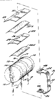
FIG. 1 is a vertically exploded perspective view of a surge arrestor
having a fail safe thermal overload mech~nism in accordance with
invention;
FIG. 2 is a end view of the arrestor and components of the overload
merh~nism in an assembled condition;
FIG. 3 is a side elevational view of the surge arrestor;
FIG. 4 is a top plan view of the assembly of Fig. 2, showing in
phantom lines a solder billet whose opposite ends are spaced from line
electrodes at opposite ends of the arrestor housing;
FIG. 5 is a view simil~r to Figure 4 showing in phantom lines a
solder billet whose ends extend to electrodes at opposite ends of the body of
the arrestor;
FIG. 6 is a fragmentary end view of the arrestor housing and of a
solder billet and overlying rh~nnel member of the fail safe me~h~ni~m;
FIG. 7 is a view ~imil~r to Fig. 6, but showing the components in
positions assumed during a thermal overload; and
FIG. 8 is a view simil~r to Fig. 6 showing gel or other protective
wo 94/00864 PCr/US93/06361
213 93 ~1 4
sealant material encapsulating the arrestor and components of the fail
safe mech~nism.
Description of the Illustrated Embodiment
The surge arrestor 10 shown in the drawings is illustratively of a
known type having a cylindrical housing 12 that includes disk-shaped
line electrodes 14 at its opposite ends, a disk-shaped ground electrode 16
intermediate the length of the housing, and insulating material 17
intermediate electrode 16 and each of the line electrodes 14. Arrestor 10
may and illustratively does further include pin-type lead elements 18 that
extend downwardly from respective ones of the electrodes. At least some,
and illustratively subst~nti~lly all, of the exterior surface of housing 12 is
overlaid by a film, foil or coating of solder flux material 20 which is
indicated in the drawings by stippling. Flux material 20 is preferably of a
rosin-based type that under normal temperatures of housing 12 has
strong dielectric properties, and protects the housing and other members
engaged thereby from cont~min~nts and other materials such as soft
textured encapsulants 44 (e.g., gels, oils, greases, etc.) such as shown in
Fig. 8. Under thermal overload conditions the flux greatly facilitates flow
of molten solder along the housing and other members engaged thereby.
Flux of the foregoing type is sold by M. W. Dunton Co. of Providence,
Rhode Island, under the trademark ELECTRO-ROSIN RA50, and is
comprised essentially of natural rosin, alcohol and proprietary
activators.
A channel-shaped solder billet 22 overlies and extends
longitudinally of the upper surface of housing 12. Billet 22 is
illustratively of inverted V-shaped configuration and has opposite side
sections that extend angularly downwardly from each other and from an
apex 24 upon the upper surface of the billet. The undersurface of the
billet preferably and illustratively has a concave contour complementary
to the cylindrical outer surface of housing 12, and may have a film or
coating 20-1 of flux 20 thereon. The thickness of billet 22 is greatest in the
WO 94/00864 PCr/US93/06361
- 5 2139327
portion thereof underlying apex 24 and is of a lesser magnitude adjacent
the opposite side edges of the billet. The upper surface of the billet has a
semispherical protuberance 26 generally centrally thereof, and may have
a foil, film or co~ting 20-2 of flux 20 upon such upper surface.
Alternatively or additionally, flux material 20-2 may be present
upon the unde~su~face of a conductive channel member 28 of the ther~nal
overload merh~nism. In keeping with billet 22, member 28 is preferably
of generally channel-like V-shaped configuration, and has opposite side
sections that closely overlie the opposite side sections of billet 22. A
centrally located semispherical socket 30 upon the upper surface of
member 28 receives billet protuberance 26 and allows limited adjustive
movement of billet 22 relative to plate 28 and arrestor housing 12.
The aforesaid components of FIG. 1 are secured to each other and
to arrestor housing 12 by a generally U-shaped resilient spring member
32. Spring 32 has generally horizontally exten~ling upper and lower legs
34, 36 that extend in parallel relationship to each other from a generally
vertically extending section 38. Legs 34, 36 have vertically aligned
openings 40, 42 adjacent their free outer ends. The center one of the
conductive pins 18 e~ten~ downwardly through opening 42 of leg 36 of
arrestor housing 12. Opening 40 of upper spring leg 34 receives the
protuberance 30 of r~h~nnel member 28, and permits limited adjustive
movement of plate 30 and underlying solder billet 22 relative to arrestor
housing 12 and spring 32. Spring forces imposed by spring 32 upon the
assembled components bias member 28 and billet 22 downwardly to a
position wherein billet 22 is firmly seated upon the upper surface of
arrestor housing 12.
As is best shown in Figs. 4-6 of the drawings, the opposite side
edges of member 28 preferably extend beyond the opposite side edges of
the underlying solder billet 22, and the opposite end portions of member
28 preferably extend beyond the opposite ends of billet 28 and the opposite
ends of arrestor housing 12 In the embodiment of Fig. 5 the central
portion of billet 22 overlies ground electrode 16 of arrestor 10, and opposite
end portions of billet 22 overlie respective adjacent ones of line electrodes
14 of arrestor housing 12.
wo 94/00864 PC~/USg3/06361
~9~?~ 6
The embodiment of Fig. 4 differs from that of Fig. 5 primarily in
that the opposite ends of billet 22 portions are spaced axially from, and do
not overlie, electrodes 14. Consequently, while the solder flux employed
in the Fig. 4 embodiment may be of the previously described flux 20 type,
6 other flux not having the dielectric insulating properties of flux 20 may
instead be used in the embo~iment of Fig. 5.
When the arrestor 10 of Fig. 4 is subjected to thermal overload
solder billet 22 melts and molten solder from the billet flows axially, as
well as in other directions, along the exterior surface of arrestor housing
o 12 into engagement with line electrodes 14 so as to thereby est~bli~h a
dense and highly conductive short circuit between each of such
electrodes and the ground electrode 16 underlying the billet. When the
solder flux is of the preferred type that causes the molten solder to
thoroughly wet housing 12 of arrestor 10, the molten solder will flow not
5 only to the annular surfaces of the electrodes, but also to the outer end
surfaces of line electrodes 14. This will normally occur irrespective of the
orientation of arrestor housing 12.
The axial flow of molten solder from billet 22 is enhanced by the
generally V-shaped configuration of ~h~nnel member 28. As is shown in
20 Fig. 6, the opposite side edges of member 28 preferably ~ten~l outwardly
beyond the opposite side edges of billet 22, and normally are spaced
slightly above the underlying cylindrical surface of arrestor housing 12.
When solder billet 22 melts in response to a thermal overload condition,
molten solder passes initially from both the opposite ends and the
25 opposite sides of the billet and ch~nnel memher 28. This initial passage of
molten solder from the billet, in conjunction with the downward biasing
force imposed upon member 28 by spring 32, causes plate 28 to descend
until its opposite side edge portions engage the underlying surfaces of
arrestor housing 12. Such engagement restricts, if not altogether stops,
30 the passage of molten solder from beneath the opposite side edge portions
of member 28, which in turn causes preferential flow of the molten solder
parallel to the central axis of arrestor housing 12 through the opposite
ends of the space overlaid by roof 28 and to electrodes 14.
While in the illustrative embodiments the solder flux 20 is provided
wo 94t00864 PCr/US93/06361
- 7 21393~7 --
upon subst~nti~lly all of the exterior surfaces of arrestor housing 12, the
flux might instead be applied, in bands or the like, only to selected
surfaces of the housing upon which solder is to flow.
In lieu of solder flux that is applied separately, the solder flux may
5 be integral with the solder material of billet 22.
While preferred embodiments of the invention have been shown
and described, this was for purposes of illustration only, and not for
purposes of limitation, the scope of the invention being in accordance
with the following claims.