Language selection

Search

Patent 2139557 Summary

Third-party information liability

Some of the information on this Web page has been provided by external sources. The Government of Canada is not responsible for the accuracy, reliability or currency of the information supplied by external sources. Users wishing to rely upon this information should consult directly with the source of the information. Content provided by external sources is not subject to official languages, privacy and accessibility requirements.

Claims and Abstract availability

Any discrepancies in the text and image of the Claims and Abstract are due to differing posting times. Text of the Claims and Abstract are posted:

  • At the time the application is open to public inspection;
  • At the time of issue of the patent (grant).
(12) Patent: (11) CA 2139557
(54) English Title: ELECTRICAL CONNECTORS
(54) French Title: CONNECTEURS ELECTRIQUES
Status: Expired and beyond the Period of Reversal
Bibliographic Data
(51) International Patent Classification (IPC):
  • H01R 13/24 (2006.01)
  • B60R 16/02 (2006.01)
(72) Inventors :
  • BAILEY, WILLIAM R. (United States of America)
  • GARAY, ANTONIO A. (United States of America)
  • ROSBOROUGH, KEITH A. (United States of America)
(73) Owners :
  • CINCH CONNECTORS, INC.
(71) Applicants :
  • CINCH CONNECTORS, INC. (United States of America)
(74) Agent: AVENTUM IP LAW LLP
(74) Associate agent:
(45) Issued: 2000-02-29
(22) Filed Date: 1995-01-04
(41) Open to Public Inspection: 1995-07-15
Examination requested: 1996-03-07
Availability of licence: N/A
Dedicated to the Public: N/A
(25) Language of filing: English

Patent Cooperation Treaty (PCT): No

(30) Application Priority Data:
Application No. Country/Territory Date
08/182,641 (United States of America) 1994-01-14

Abstracts

English Abstract


Electrical connector devices are provided for
interconnecting external conductors with a connecting member such
as a circuit which has upwardly projecting components that are
adjacent contact areas on an exposed surface. The connector
device comprises an insulator body for supporting a plurality of
conductor elements in spaced relation to one another. The
insulator body includes a plurality of cantilever hollow
projections which have a length that exceeds the height of the
components above the contact surfaces. The projections extend
from the conductor sites generally parallel to one another and
are disposed to mate the contact surfaces while providing spaces
therearound to receive and accommodate the components. The
insulator body preferably is a unitary molded body which includes
the projections. An axially compressible conductive means
extends through each of the hollow projections from the
respective conductor site to an exposed end at the distal end of
the respective projection. Preferably each compressible
conductive means includes a wadded wire contact button and an
exposed end plunger.


Claims

Note: Claims are shown in the official language in which they were submitted.


THE EMBODIMENTS OF THE INVENTION IN WHICH AN EXCLUSIVE PROPERTY
IS CLAIMED ARE DEFINED AS FOLLOWS:
1. An electrical connector device for connecting with a
mating connector member that has a mating face which includes
generally planar conductive contact surfaces and components
adjacent such contact surfaces which extend upwardly above such
contact surfaces, said connector device comprising:
a molded insulator body including a wall having a surface
exposed toward a receiving position for supporting such a mating
connector member in generally parallel spaced relation to said
wall surface with such components therebetween, said insulator
body defining conductor positions for a plurality of spaced
electrically conductive members behind said wall surface and
further including a plurality of projections which are aligned
with said conductor positions and extend from said wall surface
generally normal thereto a distance which exceeds the extension
of such components above such contact surfaces of such a mating
member;
each of said projections and the respective adjacent portion
of said wall defining an aperture extending from the respective
conductor position to the distal end of said projection;
electrically conductive contact means extending through each
of said apertures and exposed at the distal end of the respective
projection for contacting a conductive member in the respective
conductor position while also contacting a contact surface
adjacent said distal end, said electrically conductive contact
means including a resiliently compressible element in each of
said apertures which permits resilient compressive retraction of
the conductive contact means at said distal end; and
11

said projections being disposed in a predetermined array
which corresponds to the array of the contact surfaces of such
a mating connector member;
whereby conductive members in said conductor positions are
electrically connected to the contact surfaces of such a mating
connector member through said projections and such upwardly
extending components of said mating connector member are
accommodated beside said projections.
2. The invention as in claim 1 including a plurality of
electrically conductive members in said conductor positions.
3. The invention as in claim 2 wherein said electrically
conductive members are embedded in said wall.
4. The invention as in claim 1 wherein said body includes
electrical sockets and including electrically conductive members
which extend from said sockets and traverse respective ones of
said apertures.
5. The invention as in claim 4 wherein said body defines
a well having an open side, said wall being at the bottom of said
well and said projections extending from said wall toward said
open side.
6. The invention as in claim 5 wherein said body defines
a planar surface around the open side of said well.
12

7. The invention as in claim 6 wherein the distal ends of
said projections are within said well, between said wall surface
and said planar surface.
8. The invention as in claim 1 wherein each of said
electrically conductive contact means includes a wadded wire
button element having one end exposed for abutting such an
electrically conductive member in the respective conductor
position and a plunger element abutting the other end of said
wadded wire button element and extending from said distal end of
the respective projection, said plunger element being resiliently
reciprocal along the respective aperture by the resilient spring
action of said wadded wire button element for yieldable
compressive engagement with an adjacent contact surface.
9. The invention as in claim 1 wherein said body includes
support sections defining said receiving position, said support
sections and said projections being spaced from one another for
accommodating the upwardly extending components of said mating
connector member therebetween.
10. The invention as in claim 9 wherein said support
sections form side walls of said recess.
11. The invention as in claim 10 wherein said side walls
are unitary with said wall of said body.
12. The invention as in claim 1 wherein said body defines
13

a recess with said wall surface forming the inner end of said
recess, said projections extending into said recess from said
wall surface.
13. An electrical connector combination comprising:
a connector member having a mating face that includes
generally planar conductive contact surfaces and components
adjacent such contact surfaces, said components extending
upwardly above said contact surfaces; and
a molded insulator body including a wall having a
surface exposed toward a receiving position for supporting said
connector member in generally parallel spaced relation to said
wall surface with said components therebetween, said insulator
body defining conductor positions for supporting a plurality of
spaced electrically conductive members behind said wall surface
and further including a plurality of projections which are
aligned with said conductor positions and extend from said wall
surface generally normal thereto a distance which exceeds the
extension of said components above such contact surfaces of said
connector member;
each of said projections and the respective adjacent portion
of said wall defining an aperture extending from the respective
conductor position to the distal end of said projection;
electrically conductive contact means extending through each
of said apertures and exposed at the distal end of the respective
projection for contacting a conductive member in the respective
conductor position while contacting one of said contact surfaces
adjacent said distal end, said electrically conductive contact
14

means including a resiliently compressive element in each of said
apertures which permits resilient compressive retraction of the
conductive contact means at said distal end; and
said projections being disposed in a predetermined array
which corresponds to the array of the contact surfaces of said
connector member;
whereby conductive members in said conductor positions are
electrically connected to the contact surfaces of said connector
member through said projections and said upwardly extending
components of said connector member are accommodated beside said
projections.
14. An automotive control device comprising an electrical
connector combination as in claim 13 wherein said connector
member is an automotive engine control circuit.
15. The invention as in claim 14 wherein said circuit is
mounted on a metal heat conductive plate, said body and said
plate having cooperative seating means for joining said plate and
said body with said contact surfaces of said connector member in
compressive registered relation with contact means at the distal
ends of said projections.
16. The invention as in claim 13 including a plurality of
electrically conductive members in said conductor positions.
17. The invention as in claim 16 wherein said electrically

conductive members are embedded in said wall.
18. The invention as in claim 13 wherein said body includes
electrical sockets and including electrically conductive members
which extend from said sockets and traverse respective ones of
said apertures.
19. The invention as in claim 18 wherein said body defines
a well having an open side, said wall being at the bottom of said
well and said projections extending from said wall toward said
open side.
20. The invention as in claim 19 wherein said body defines
a planar surface around the open side of said well.
21. The invention as in claim 20 wherein the distal ends
of said projections are within said well, between said wall
surface and said planar surface.
22. The invention as in claim 13 wherein each of said
electrically conductive contact means includes a wadded wire
button element having one end exposed for abutting such an
electrically conductive member in the respective conductor
position and a plunger element abutting the other end of said
wadded wire button element and extending from said distal end of
the respective projection, said plunger element being resiliently
reciprocal along the respective aperture by the resilient spring
action of said wadded wire button element for yieldable
16

compressive engagement with an adjacent contact surface.
23. The invention as in claim 13 wherein said body includes
support sections defining said receiving position, said support
sections and said projections being spaced from one another for
accommodating the upwardly extending components of said mating
connector member therebetween.
24. The invention as in claim 23 wherein said support
sections form side walls of said recess.
25. The invention as in claim 24 wherein said side walls
are unitary with said wall of said body.
26. The invention as in claim 13 wherein said body defines
a recess with said wall surface forming the inner end of said
recess, said projections extending into said recess from said
wall surface.
17

27. An electrical connector device for connecting with
a mating connector member that has, on one side thereof,
generally planar conductive contact surfaces and outwardly
projecting circuit components, said connector device
comprising:
an electrical insulator body which has a mounting side
that includes a support surface for supporting such a connector
member and a recess which extends inward of said body relative
to said support surface for receiving said outwardly protruding
circuit components of such connector member;
electrical conductors extending within said insulator
body;
said insulator body defining an opening extending from
each of said electrical conductors to an open distal end
closely adjacent the position of a conductive contact surface
of such a mating connector member supported on said support
surface;
a resilient electrically conductive contact disposed in
each of said openings and retained and supported in said
insulator body, each of said resilient electrically conductive
contacts having a proximal end engaging the respective
conductor and a distal end exposed through said distal end of
the respective opening and being resiliently compressible
axially of the respective opening for compressive engagement
with a contact surface of such a mating connector member
supported on said surface.
28. A connector device as in claim 27 wherein said
insulator body includes an outwardly facing external surface
which faces such a mating connector body mounted on said body,
and said electrical conductor elements are embedded in said
body adjacent said external surface.
29. A connector device as in claim 28 wherein said
electrical conductor elements are elongated elements which
extend generally parallel to said external surface.
18

30. A connector device as in claim 28 wherein said
external surface is a surface of a wall of said body which
forms the bottom of said recess whereby said circuit components
are accommodated between said connector member and said
external surface.
31. A connector device for interconnecting external
circuits with a mating connector member which includes
electrical conductors and has a mating face that includes at
least one exposed generally planar conductive contact surface,
said connector device comprising:
an electrical insulator body for supporting at least one
conductor element and having an external surface for receiving
such a mating connector member thereover with said planar
conductive contact surface exposed toward said electrical
insulator body,
at least one electrical conductor element which includes
a portion disposed within said insulator body and a prong
extending externally of said body for engagement by a conductor
of an external circuit,
said insulator body defining an opening extending from
each said electrical conductor element therein to an open
distal end closely adjacent the position of such a mating
connector member supported on said device, and
a resilient electrically conductive contact disposed in
each of said openings and retained and supported in said
insulator body, each of said resilient electrically conductive
contacts having a proximal end engaging the respective
conductor and a distal end exposed through said distal end of
the respective opening and being resiliently compressible
axially of the respective opening for compressive engagement
with a contact surface of such a mating connector member
mounted on said device.
32. A connector device as in claim 31 wherein each of
said openings has an inner side wall and each of said resilient
19

conductive contacts is supported by the inner side wall of the
respective opening.
33. A connector device as in claim 31 wherein each of
said resilient conductive contacts includes a wadded wire
button element.
34. A connector device as in claim 31 wherein each of
said resilient conductive contacts includes a plurality of
elements and at least one of said elements is a wadded wire
button element.
35. A connector device as in claim 31 wherein each of
said resilient conductive contacts includes a wadded wire
button element which has one end abutting the respective
conductor element and a plunger element abutting the other end
of said wadded wire button element, said plunger element being
resiliently reciprocable axially of the respective opening by
the respective wadded wire button element.
36. A connector device as in claim 31 for interconnecting
with such a mating connector member which also has outwardly
projecting circuit components on the same side thereof as said
planar conductive contact surface, wherein said insulator body
includes portions for supporting such a mating connector member
in spaced relation to said external surface to accommodate said
circuit components between said connector member and said
external surface.
37. A connector device as in claim 36 wherein said
electrical conductor element is embedded in said body adjacent
said external surface.
38. A connector device as in claim 37 wherein said
electrical conductor element is an elongated element which
extends generally parallel to said external surface.

39. A connector device for interconnecting external
circuits with a mating connector member which includes
electrical conductors and has a mating face that includes
generally planar conductive contact surfaces, said connector
device comprising:
an electrical insulator body having one wall with an
external surface for receiving such a mating connector member
thereover,
at least one externally prong element exposed for
engagement by a conductor of an external circuit connector,
an electrical conductor joined to each of said prong
elements and extending within said insulator body adjacent said
wall,
said insulator body defining openings extending from said
electrical conductors through said wall surface, and
a resilient electrically conductive contact disposed in
each of said openings and retained and supported in said
insulator body, each of said resilient electrically conductive
contacts having a proximal end engaging the respective
conductor and a distal end exposed through said wall surface
and being resiliently compressible axially of the respective
opening for compressive engagement with a contact surface of
such a mating connector member disposed over said wall surface.
40. A connector device as in claim 39 wherein said
electrical conductor is an elongated conductor disposed within
said insulator body generally parallel to said external
surface.
41. A connector device as in claim 39 wherein each of
said openings has an inner side wall and each of said resilient
conductive contacts is supported by the inner side wall of the
respective opening.
21

42. A connector device as in claim 39 wherein each of
said resilient conductive contacts includes a wadded wire
button element.
43. A connector device as in claim 39 wherein each of
said resilient conductive contacts includes a plurality of
elements and at least one of said elements is a wadded wire
button element.
44. A connector device as in claim 39 wherein each of
said resilient conductive contacts includes a wadded wire
button element which has one end abutting the respective
conductor and a plunger element abutting the other end of said
wadded wire button element, said plunger element being
resiliently reciprocable axially of the respective opening by
the respective wadded wire button element.
45. A connector device as in claim 39 wherein said
insulator body includes an externally exposed socket, a
plurality of said prong elements extending within said socket
and a corresponding plurality of electrical conductors
connected to said prong elements and extending within said
insulator body.
46. A connector device as in claim 45 wherein said
electrical conductors are integral with the respective prong
element.
47. An electrical connector assembly comprising:
a connector member that has, on one side thereof,
generally planar conductive contact surfaces and outwardly
projecting circuit components;
an electrical insulator body which has a mounting side
that includes a support surface, said connector member being
supported on said support surface, said body having a recess
which extends inward of said body relative to said support
22

surface and in which said outwardly protruding circuit
components of such connector member are disposed;
electrical conductors extending within said insulator
body;
said insulator body including portions which extend from
adjacent said electrical connectors to adjacent said conductive
contact surfaces of said connector member and define an opening
extending from each of said electrical conductors to an open
distal end closely adjacent the position of a respective one
of said conductive contact surfaces; and
a resilient electrically conductive contact disposed in
each of said openings, each of said resilient electrically
conductive contacts having a proximal end engaging the
respective conductor and a distal end engaging the respective
contact surface, said conductive contact elements being
resiliently compressible axially of the respective opening for
compressive engagement with the respective contact surface of
said mating connector member.
48. An electrical connector assembly as in claim 47 in
which said connector member includes a heat sink and a circuit
mounted on said heat sink, said circuit including said
generally planar contact surfaces and said outwardly protruding
circuit components.
49. A connector device as in claim 47 wherein each of
said resilient conductive contacts includes a plurality of
elements and at least one of said elements is a wadded wire
button element.
50. A connector device as in claim 47 wherein each of
said resilient conductive contacts includes a wadded wire
button element which has one end abutting the respective
conductor element and a plunger element abutting the other end
of said wadded wire button element, said plunger element being
23

resiliently reciprocable axially of the respective opening by
the respective wadded wire button element.
24

Description

Note: Descriptions are shown in the official language in which they were submitted.


213955'
1162-37
ELECTRICAL CONNECTORS
This invention relates to electrical connectors and
particularly to electrical connector devices for making direct
connections between a plurality of external conductors and the
leads on a device which has exposed contact areas and adjacent
components that extend above the contact areas, such as on a
hybrid circuit or printed circuit board. The illustrated
preferred embodiment is an engine control connector assembly for
mounting and connecting a control circuit to an automotive
engine.
Background of the Invention
Hybrid circuits, integrated circuit chips, printed circuit
boards and like devices, which will be referred to as circuits,
often have discrete circuit components mounted on and extending
above a major planar surface. Conductor traces disposed
internally of the device or on its surface interconnect the
components and provide access for connection to external circuit
conductor leads. In various uses of such devices, a surface on
which the components are mounted presents the most readily
accessible area for joining external conductors. one example
is in automotive engine connector devices wherein a control
circuit or hybrid circuit is mounted on a heat sink plate. In
the past, wire leads were soldered or welded to contact lugs
provided on the front face of the control device, between
upstanding circuit components, and to external connector leads
in the connector device.
The soldered or welded connection techniques are tedious and
expensive. For example, the soldered or.welded connections are
1

~"
~ f 3~S S ~
prone to failure during the manufacturing of the device and
during the use of the device by the customer. These failures
result in higher manufacturing costs due to rejects and in higher
costs due to warranty claims and customer dissatisfaction. The
failure or the reduction in the integrity of the soldered or
welded connections can occur due to vibration, shock, thermal
stress and mechanical stress. 1~urthermore, the manufacture and
assembly of the devices, including the soldering or welding
operation, is time consuming and expensive in comparison tv the
to present invention.
In addition, the upstanding components on the exposed
surfaces of such devices present impediments to application of
alternative simplified connective techniques, e.g. such as are
disclosed ~n U.S. 1?atents 4,988,306, 4,992,053, 5,013,249
5,127,837.
It is an object of this invention to provide improved
connector devices and connectors for effecting electrical
connections with chips, circuits and boards bearing upstanding
components as referred to above.
It is a further object of this invention to provide such
connector davices and connectors by which such connections can
be effected easily and inexpensively.
Summary of the Inyention
Electrical connector devices are provided for
interconnecting external conductors with a connecting member such
as a circuit which has upwardly projecting components that are
adjacent contact areas on an exposed surface. The connector
device comprises an lnsul.ator body for supporting a plurality of
2

conductor elements in spaced relation to one another. The
insulator body includes a plurality of cantilever hollow
projections which have a length that exceeds the height of the
components above the contact surfaces. The projections extend
from the conductor sites generally parallel to one another and
are disposed to mate the contact surfaces while providing spaces
therearound to receive and accommodate the components. The
insulator body preferably is a unitary molded body which includes
the projections. An axially compressible conductive means
extends through each of the hollow projections from the
respective condutctor site to an exposed end at the distal end of
the respective projection. Preferably each compressible
conductive means includes a wadded wire contact button and an
exposed end plunger. Direct conductive connection between the
external conductors and the contact surfaces of the connecting
memb~_r are obtained by pressing the connector device and
connecting member together with the projections aligned with the
contact surfaces and the components being accommodated beside the
pro j ection .
In one aspect, the present invention provides an
electrical connector device for connecting with a
mating connector member that has a mating face which includes
generally planar conductive contact surfaces and components
adjacent such contact surfaces which extend upwardly above such
contact surfaces, said connector device comprising:
-3-
CA 02139557 1999-11-30 '

a molded insulator body including a wall having a surface
exposed toward a receiving position for supporting such a mating
connector member in generally parahlel spaced relation to said
wall surface with such components therebetween, said insulator
body defining conductor positions for a plurality of spaced
electrically conductive members behind said wall surface and
further including a plurality of projections which are aligned
with said conductor positions. and extend from said wall surface
generally normal thereto a distance which exceeds the extension
of such components above such contact surfaces of such a mating
member;
each of said pro jec:tions and the respective adjacent portion
of said wall defining mo aperture extending from the respective
conductor position to the distal end of said projection;
electrically conductive contact means extending through each
of said apertures and exposed at the distal end of the respective
projection for contacting a conductive member in the respective
conductor position while also contacting a contact surface
adjacent said distal end, said electrically conductive contact
means including a resiliently compressible element in each of
said apertures which permits resilient compressive retraction of
the conductive contact means at said distal end; and
said projections being disposed in a predetermined array
which corresponds to the array of the contact surfaces of such
a mating connector member;
whereby conductive members in said conductor positions are
electrically connected to~the contact surfaces of such a mating
connector member through said projections and such upwardly
extending components of said mating connector member are
accommodated beside said projections.
--3A-
CA 02139557 1999-11-30

In another aspect, the present invention provides an
electrical connector combination comprising:
a connector member having a mating face that includes
generally planar conductive contact surfaces~ and components
adjacent such contact surfaces, said components extending
upwardly above said contact surfaces; and
a molded insulator body including a wall having a
surface exposed toward a receiving position for supporting said
connector member in generally parallel spaced relation to said
wall surface with said components therebetween, said insulator
body defining conductor positions for supporting a plurality of
spaced electrically conductive members behind said wall surface
and further including a plurality of projections which are
aligned with said conductor positions and extend from said wall
surface generally normal thereto a distance which exceeds the
extension of said components above such contact surfaces of said
connector member;
each of said projections and the respective adjacent portion
of said wall defining an aperture extending from the respective
conductor posLtion to the distal end of said projection;
electrically conductive contact means extending through each
of said apertures and exposed at the distal end of the respective
projection for contacting a conductive member in the respective
conductor position while contacting one of said contact surfaces
adjacent said distal end, said electrically conductive contact
means including a resiliently compressive element in each of said
apertures which permits resilient compressive retraction of the
conductive contact means at said distal end; and
said projections being disposed in a predetermined array
which corresponds to the array of the contact surfaces of said
connector member;
3;3
CA 02139557 1999-11-30

whereby conductive members in said conductor positions are
electrically connected to the contact surfaces of said connector
... member through said projections and said upwardly extending
components of said connector member are accommodated beside said
projections.
In a further aspect, the present invention provides an
automotive control device comprising the aforesaid electrical
connector combination, wherein the connector member is an
automotive engine control circuit.
In a still further aspect, the present invention provides
an electrical connector device for connecting with a mating
connector member that has, on one side thereof, generally
planar conductive contact surfaces and outwardly projecting
circuit components, the connector device comprising:
an electrical insulator body which has a mounting side
that includes a support surface for supporting such a connector
member and a recess which extends inward of the body relative
to the support surface for receiving the outwardly protruding
circuit components of such connector member;
electrical conductors extending within the insulator body
the insulator body defining an opening extending from each
of the electrical conductors to an open distal end closely
adjacent the position of a conductive contact surface of such
a mating connector member supported on the support surface;
a resilient electrically conductive contact disposed in
each of the openings and retained and supported in the
insulator body, each of the resilient electrically conductive
contacts having a proximal end engaging the respective
conductor and a distal end exposed through the distal end of
the respective opening and being resiliently compressible
axially of the respective opening for compressive engagement
with a contact surface of such a mating connector member
supported on the surface.
-3C-
CA 02139557 1999-11-30

Conveniently, the insulator body includes an outwardly
facing external surface which faces such a mating connector
body mounted on the body, and the electrical conductor elements
are embedded in the body adjacent the external surface. In one
variation, the electrical conductor elements are elongated
elements which extend generally parallel to the external
surface. In another variation the external surface is a
surface of a wall of the body which forms the bottom of the
recess whereby the circuit components are accommodated between
the connector member and the external surface.
In a further aspect, the present invention provides a
connector device for interconnecting external circuits with a
mating connector member which includes electrical conductors
and has a mating face that includes at least one exposed
generally planar conductive contact surface, the connector
device comprising:
an electrical insulator body for supporting at least one
conductor element and having an external surface for receiving
such a mating connector member thereover with the planar
conductive contact surface exposed toward the electrical
insulator body,
at least one electrical conductor element which includes
a portion disposed within the insulator body and a prong
extending externally of the body for engagement by a conductor
of an external circuit,
the insulator body defining an opening extending from each
electrical conductor element therein to an open distal end
closely adjacent the position of such a mating connector member
supported on the device, and
a resilient electrically conductive contact disposed in
each of the openings and retained and supported in the
insulator body, each of the resilient electrically conductive
contacts having a proximal end engaging the respective
conductor and a distal end exposed through the distal end of
-3D-
CA 02139557 1999-11-30

the respective opening and being resiliently compressible
axially of the respective opening for compressive engagement
with a contact surface of such a mating connector member
mounted on the device.
In one variation each of the openings has an inner side
wall and each of the resilient conductive contacts is supported
by the inner side wall of the respective opening.
In a still further variation each of the resilient
conductive contacts includes a wadded wire button element.
In a further variation each of the resilient conductive
contacts includes a plurality of elements and at least one of
the elements is a wadded wire button element.
In a further variation each of the resilient conductive
contacts includes a wadded wire button element which has one
end abutting the respective conductor element and a plunger
element abutting the other end of the wadded wire button
element, the plunger element being resiliently reciprocable
axially of the respective opening by the respective wadded wire
button element.
In a still further variation the mating connector member
also has outwardly projecting circuit components on the same
side thereof as the planar conductive contact surface, and
wherein the insulator body includes portions for supporting
such a mating connector member in spaced relation to the
external surface to accommodate the circuit components between
the connector member and the external surface. Conveniently,
the electrical conductor element is embedded in the body
adjacent the external surface. Conveniently, the electrical
conductor element is an elongated element which extends
generally parallel to the external surface.
In a further aspect, the present invention provides a
connector device for interconnecting external circuits with a
mating connector member which includes electrical conductors
-3E-
CA 02139557 1999-11-30

and has a mating face that includes generally planar conductive
contact surfaces, the connector device comprising:
an electrical insulator body having one wall with an
external surface for receiving such a mating connector member
thereover,
at least one externally prong element exposed for
engagement by a conductor of an external circuit connector,
an electrical conductor joined to each of the prong
elements and extending within the insulator body adjacent the
wall,
the insulator body defining openings extending from the
electrical conductors through the wall surface, and
a resilient electrically conductive contact disposed in
each of the openings and retained and supported in the
insulator body, each of the resilient electrically conductive
contacts having a proximal end engaging the respective
conductor and a distal end exposed through the wall surface and
being resiliently compressible axially of the respective
opening for compressive engagement with a contact surface of
such a mating connector member disposed over the wall surface.
In one variation, the insulator body includes an
externally exposed socket, a plurality of the prong elements
extending within the socket and a corresponding plurality of
electrical conductors connected to the prong elements and
extending within the insulator body. Conveniently, the
electrical conductors are integral with the respective prong
element.
In a still further aspect, the present invention provides
an electrical connector assembly comprising:
a connector member that has, on one side thereof,
generally planar conductive contact surfaces and outwardly
projecting circuit components
- 3 F-
CA 02139557 1999-11-30

a
an electrical insulator body which has a mounting side
that includes a support surface, the connector member being
supported on the support surface, the body having a recess
which extends inward of the body relative to the support
surface and in which the outwardly protruding circuit
components of such connector member are disposed
electrical conductors extending within the insulator body
the insulator body including portions which extend from
adjacent the electrical connectors to adjacent the conductive
contact surfaces of the connector member and define an opening
extending from each of the electrical conductors to an open
distal end closely adjacent the position of a respective one
of the conductive contact surfaces and
a resilient electrically conductive contact disposed in
each of the openings, each of the resilient electrically
conductive contacts having a proximal end engaging the
respective conductor and a distal end engaging the respective
contact surface, the conductive contact elements being
resiliently compressible axially of the respective opening for
compressive engagement with the respective contact surface of
the mating connector member.
Conveniently, the connector member includes a heat sink
and a circuit mounted on the heat sink, the circuit including
the generally planar contact surfaces and the outwardly
protruding circuit components.
Other objects and advantages of the invention will become
apparent upon reading the following detailed description and
appended claims, and upon reference to the accompanying drawings.
D~~.ef Descrititio of the Drawings
Fig. 1 is a perspective view of an electrical connector
employing teachings of this invention.
Fig. 2 is a perspective of the opposite side of the
connector device of Fig. 1, with the cover plate and circuit
removed.
-3G-
CA 02139557 1999-11-30

~~3~~5
Figs. 3-6 are a top view, a left side view, a right side
view and a bottom view of the connector device of Fig. 2,
respectively.
Fig. 7 is an enlarged cross-sectional view taken on line 7-7
of Fig. 3.
Fig. 8 is an enlarged longitudinal cross-sectional view
taken on irregular line 8-8 of Fig. 6, with the projection
contacts omitted.
Fig. 9 is a further enlarged partial cross-sectional and
side view of two adjacent contact projections generally as seen
along line 7-7 in Fig. 3.
Fig. 10 is a perspective view of a cover plate and a circuit
thereon for connecting with the device of Fig. 1.
Fig. 11 is an enlarged side view of a plunger contact
element of the connector of Fig. 1.
Figs. 12 and 14 are cross-sectional views corresponding to
Figs. 7 and 8 respectively, each including the circuit and plate
in position with a contact pad of the circuit beneath each of the
plunger points.
Fig. 13 is an enlarged partial cross-sectional view
corresponding to Fig. 9, with the buttons and plungers in place,
the end of the contact projections staked inward to retain the
plungers and with the corresponding portions of the plate and
circuit assembled thereagainst.
Detailed Description Of
Embodiments Of The Invention
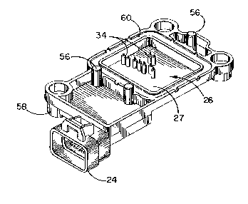
Referring to the enclosed drawings, the connector device 16
includes basically a molded frame body 20 which includes a pair
of sockets 22 and 24 and which forms a recess or a well 26 in one
4

X139557
side of the body between these sockets. Several conductor strips
28, 30 form contact prongs 28p, Sop in the sockets 22 and 24 and
extend to predetermined positions in the body wall 27 at the
inner side of the recess 26. Other than the prong-ends 28p, 30p
which are exposed for engagement with suitable plug-in types of
circuit connectors that mate in the sockets 22, 24, the
conductors 28, 30 are embedded in the molded body 20.
Within the well 26, the body 20 includes hollow cylindrical
chimney-like projections 34 which extend parallel to one another
l0 from the wall 27. One of these projections is aligned with each
of the conductors 28, 30. The body defines a bore, opening or
aperture 36 which extends from the outer distal end of each of
these projections to the respective conductor 28, 30, with the
conductor being exposed at the inner end of that bore; see
particularly Figs. 9, 12, 13 and 14.
As further illustrated in Figs. 11, 12, 13 and 14, an
axially resilient button-plunger column contact 37, comprising
a resilient wadded wire button 38 and a reciprocal plunger 40,
is mounted in each of the bores 36. The buttons 38 and plungers 40
are mounted by insertion into the open ends of the bores 36. Then
the outer ends of the projections are modified, as by cold-form
staking inwardly, as at 39 in Fig. 13, to retain the larger body
portion 41 of the plunger 40 in the respective bore 36 while
permitting free passage of the smaller diameter end portion 42 as
5

_ ~~39557
illustrated in Figs. 12, 13 and 14. The buttons 38 and plungers
40 are sufficiently freely movable axially of the bores 36 such
that the buttons 38 maintain contact with the adjacent surface
of the respective conductor 28, 30 ,and with the inward end of the
respective plunger 40 while permitting and providing resilient
axial movement of each plunger within the ambit of axial movement
corresponding generally to the length of the projecting end 42.
A metal mounting cover plate 50 as in Fig. 10 carries a
circuit 52 adhered to its inward surface. The circuit 52
includes a number of electronic control components C and
appropriate conductors (not shown) which connect those components
to one another and to contact pads 54 exposed on the inward face
of the circuit, among the electrical components C. The
conductors of the circuit 52 may be traces on the surface or
within laminations of the circuit. The location of the
.projections 34 carrying contacts 38, 40 are correlated to the
location of the respective contact pads 54 such that each
conductor 28, 30 is connected to the appropriate portion of the
::ircuit 52 when the plate 50 is mounted on the housing 20 over
the recess 26 with the circuit in appropriate registry. Because
the projections 34 are of relative small cross-section, they can
be and are appropriately located so as to traverse the recess 26
to the respective pad 54 without contacting or interfering with
Lhe various components C which extend from the circuit upwardly
:nto the recess 26 beside and among the projections 34.
The metal cover plate 50 serves as a heat sink and transfer
~~ath. Slots or openings 55 mate with pins 56 on the body 20 for
registration positioning of the plate 50 and particularly the
6

2139557
attached circuit 52 relative to the projections 34. The pins 56
extend through the openings 55 and above the plate 50. The upper
portions of the pins 56, which extend above the plate 50, are
deformed by a staking process, a rolling process, a spinning
process or another appropriate process in order to create a head
on the upper portions of the pins 56. The deformation of the
upper portions into a head secures the plate 50 and the body 20
together in mating relation. An annular shoulder surface 60 on
the body 20, around the recess 26, provides a mating seat for the
plate 50. A gasket material is applied to one or both of the
mating face 62 of the plate or the body 20 on the shoulder
surfaces 60 (Figs. 12 and 14), to assist in providing a sealed
joint therebetween. Securing means, such as screws or bolts, may
be applied through openings 58 for mounting the assembled
connector, as on an automotive engine. Appropriate circuit leads
are attached through connectors that mate at the sockets 22, 24.
Also, the recess 26 may be filled with a permanently soft potting
compound for further sealing against humidity and environmental
factors and to serve as a shock absorber to protect the various
components against vibrations applied to the connector in use,
such as when mounted on automobile engines.
The frame body 20 can be molded of a thermoplastic material.
By way of one specific illustrative example, a frame body 20 is
molded of thermoplastic glass reinforced polyester manufactured
1:~ Hoechest Celanese of 26 Main Street, Chatham, New Jersey,
i'.S.A. under compound number 3310. The body 20 was formed with
~, well 26 about 2 inches (51 mm) by about 2 inches (51 mm) in
plan and about .200 inches (5 mm) deep. The inner wall 27 was
7

213955 7
about .200 inches (5 mm) thick, with the conductors 28, 30
approximately at its mid-plane as illustrated in Figs. 7, 8 and
12-14. The side walls forming surfaces 60 were about .300 inches
(7.5 mm) thick. The projections 34 were about 0.200 inches (5
mm) long and of about 0.100 inches (2.5 mm) outside diameter,
with the apertures 36 being of circular cylindrical configuration
of about 0.045 inches (1.1 mm) inside diameter and 0.280 inches
(7 mm) length from the adjacent surface of the respective
conductor 28, 30 to the distal end of the projection. The
projections were spaced about 0.280 inches (7 mm) between rows.
The wadded buttons 38 were formed from Molybdenum wire of
.002 in (.05 mm) diameter, with each button being .110 inches
(-2.8 mm) in length and of .040 inches (1 mm) nominal outside
diameter. Each plunger 40 was formed of brass and had a
cylindrical main body 41 of about .041 inches (1 mm) outside
diameter and about .200 inches (5 mm) long, with a central axial
projection 42 of about .022 inches (0.5 mm) outside diameter and
about .060 inches (1.5 mm) long.
The circuit 52 was about 1 inch (25 mm) by 1.75 inches (44.5
mm) and .040 inches (1 mm) thick with components C extending as
much as about .100 inches (2.5 mm) from its contact surface which
carried the contact pads 54. The circuit 52 was adhered to a
planar plate 50 which was seated on the outer shoulders 60 of the
well walls. The space between the rows of the projections 34 and
the space therearound within the well 26 readily accommodated the
components C When the contact pads 54 were seated against the
resiliently retractable contact ends 42.
In the illustrated preferred embodiment the external
8

X13955 7
conductor leads 28, 30 are molded in place in the body 20.
However, it will be appreciated that the conductors may be
separately applied, as by insertion in appropriate positioning
cavities or channels on the rear wall 27 in registration with the
projections 34. It also will be appreciated that the projections
34~may be located in any desired array according to the available
locations of the contact surfaces 54 on the device to be
connected. The pattern and locations of the external conductors
28, 30 should be correspondingly adjusted to place them in
opposed relation to the respective contact surfaces 54, at the
inward ends of the apertures 36.
Plunger-button contacts have been described as preferred for
obtaining the desired axially compressive conductive contacts
because of the wearability and ruggedness of the exposed plunger
contact ends. However, other compressible contact core
arrangements may be utilized in appropriate circumstances. For
example, there may be a fixed core-piece extending from the
conductor 28, 30 to the resilient contact column components, such
as to the components 38, 40. Also, each resilient contact column
may be a single elongated wadded wire button, or a button-slug-
button arrangement or a plunger-button-plunger arrangement or other
arrangements to provide the desirable resilient compressive and
uniform conductive contact action.
It will be seen that electrical connector devices have been
provided which meet the objects aforestated. While particular
embodiments of the invention have been shown, it will be
9

understood, of course, that the invention is not limited thereto
since modifications may be made by those skilled in the art,
particularly in light of the foregoing teachings. It is,
therefore, contemplated by the appended claims to cover any such
modifications as incorporate those features which constitute the
essential features of these improvements within the true spirit
and scope of the invention.
l0

Representative Drawing
A single figure which represents the drawing illustrating the invention.
Administrative Status

2024-08-01:As part of the Next Generation Patents (NGP) transition, the Canadian Patents Database (CPD) now contains a more detailed Event History, which replicates the Event Log of our new back-office solution.

Please note that "Inactive:" events refers to events no longer in use in our new back-office solution.

For a clearer understanding of the status of the application/patent presented on this page, the site Disclaimer , as well as the definitions for Patent , Event History , Maintenance Fee  and Payment History  should be consulted.

Event History

Description Date
Inactive: Adhoc Request Documented 2018-06-06
Revocation of Agent Requirements Determined Compliant 2018-05-18
Appointment of Agent Requirements Determined Compliant 2018-05-18
Time Limit for Reversal Expired 2012-01-04
Inactive: IPC deactivated 2011-07-27
Letter Sent 2011-01-04
Inactive: Late MF processed 2009-02-12
Letter Sent 2009-01-05
Inactive: IPC from MCD 2006-03-11
Inactive: First IPC derived 2006-03-11
Inactive: IPC from MCD 2006-03-11
Inactive: Late MF processed 2004-01-09
Letter Sent 2001-04-05
Grant by Issuance 2000-02-29
Inactive: Cover page published 2000-02-28
Letter Sent 1999-12-22
Amendment After Allowance Requirements Determined Compliant 1999-12-22
Inactive: Final fee received 1999-11-30
Pre-grant 1999-11-30
Inactive: Amendment after Allowance Fee Processed 1999-11-30
Amendment After Allowance (AAA) Received 1999-11-30
Notice of Allowance is Issued 1999-06-07
Letter Sent 1999-06-07
Notice of Allowance is Issued 1999-06-07
Inactive: Approved for allowance (AFA) 1999-05-14
Inactive: Status info is complete as of Log entry date 1998-04-21
Inactive: Application prosecuted on TS as of Log entry date 1998-04-21
All Requirements for Examination Determined Compliant 1996-03-07
Request for Examination Requirements Determined Compliant 1996-03-07
Application Published (Open to Public Inspection) 1995-07-15

Abandonment History

There is no abandonment history.

Maintenance Fee

The last payment was received on 1999-12-14

Note : If the full payment has not been received on or before the date indicated, a further fee may be required which may be one of the following

  • the reinstatement fee;
  • the late payment fee; or
  • additional fee to reverse deemed expiry.

Patent fees are adjusted on the 1st of January every year. The amounts above are the current amounts if received by December 31 of the current year.
Please refer to the CIPO Patent Fees web page to see all current fee amounts.

Fee History

Fee Type Anniversary Year Due Date Paid Date
Request for examination - standard 1996-03-07
MF (application, 3rd anniv.) - standard 03 1998-01-05 1997-12-16
MF (application, 4th anniv.) - standard 04 1999-01-04 1998-12-29
Final fee - standard 1999-11-30
1999-11-30
MF (application, 5th anniv.) - standard 05 2000-01-04 1999-12-14
MF (patent, 6th anniv.) - standard 2001-01-04 2000-12-20
Registration of a document 2001-03-05
MF (patent, 7th anniv.) - standard 2002-01-04 2002-01-03
MF (patent, 8th anniv.) - standard 2003-01-06 2002-12-18
MF (patent, 9th anniv.) - standard 2004-01-05 2004-01-09
Reversal of deemed expiry 2009-01-05 2004-01-09
MF (patent, 10th anniv.) - standard 2005-01-04 2004-12-29
MF (patent, 11th anniv.) - standard 2006-01-04 2005-12-07
MF (patent, 12th anniv.) - standard 2007-01-04 2006-12-08
MF (patent, 13th anniv.) - standard 2008-01-04 2007-12-31
MF (patent, 14th anniv.) - standard 2009-01-05 2009-02-12
Reversal of deemed expiry 2009-01-05 2009-02-12
MF (patent, 15th anniv.) - standard 2010-01-04 2009-12-16
Owners on Record

Note: Records showing the ownership history in alphabetical order.

Current Owners on Record
CINCH CONNECTORS, INC.
Past Owners on Record
ANTONIO A. GARAY
KEITH A. ROSBOROUGH
WILLIAM R. BAILEY
Past Owners that do not appear in the "Owners on Record" listing will appear in other documentation within the application.
Documents

To view selected files, please enter reCAPTCHA code :


To view images, click a link in the Document Description column. To download the documents, select one or more checkboxes in the first column and then click the "Download Selected in PDF format (Zip Archive)" or the "Download Selected as Single PDF" button.

List of published and non-published patent-specific documents on the CPD .

If you have any difficulty accessing content, you can call the Client Service Centre at 1-866-997-1936 or send them an e-mail at CIPO Client Service Centre.


Document
Description 
Date
(yyyy-mm-dd) 
Number of pages   Size of Image (KB) 
Description 1995-07-14 10 377
Abstract 1995-07-14 1 32
Claims 1995-07-14 7 237
Drawings 1995-07-14 4 142
Claims 1996-03-06 14 503
Description 1996-03-06 10 374
Abstract 1998-05-06 1 32
Description 1999-11-29 17 736
Representative drawing 2000-01-30 1 17
Commissioner's Notice - Application Found Allowable 1999-06-06 1 165
Late Payment Acknowledgement 2004-02-03 1 168
Maintenance Fee Notice 2009-02-15 1 171
Late Payment Acknowledgement 2009-03-01 1 164
Maintenance Fee Notice 2011-02-14 1 171
Correspondence 1995-02-20 15 508
Correspondence 1999-11-29 2 58
Correspondence 1999-12-21 1 6
Fees 1998-12-28 1 39
Fees 1997-12-15 1 40
Fees 1999-12-13 1 35
Fees 2004-12-28 1 34
Fees 1996-12-17 1 46