Language selection

Search

Patent 2141560 Summary

Third-party information liability

Some of the information on this Web page has been provided by external sources. The Government of Canada is not responsible for the accuracy, reliability or currency of the information supplied by external sources. Users wishing to rely upon this information should consult directly with the source of the information. Content provided by external sources is not subject to official languages, privacy and accessibility requirements.

Claims and Abstract availability

Any discrepancies in the text and image of the Claims and Abstract are due to differing posting times. Text of the Claims and Abstract are posted:

  • At the time the application is open to public inspection;
  • At the time of issue of the patent (grant).
(12) Patent: (11) CA 2141560
(54) English Title: METHOD AND CIRCUIT ARRANGEMENT FOR ELECTRIC COMPENSATION OF SIGNAL DISTORTION CAUSED BY LASER CHIRP AND FIBER DISPERSION
(54) French Title: METHODE ET CIRCUIT POUR CORRIGER LA DISTORSION CAUSEE DANS LES SIGNAUX PAR LES GLISSEMENTS DE FREQUENCE LASER ET LA DISPERSION DANS LES FIBRES
Status: Expired and beyond the Period of Reversal
Bibliographic Data
(51) International Patent Classification (IPC):
(72) Inventors :
  • GOTTWALD, ERICH (Germany)
(73) Owners :
  • SIEMENS AKTIENGESELLSCHAFT
(71) Applicants :
  • SIEMENS AKTIENGESELLSCHAFT (Germany)
(74) Agent: SMART & BIGGAR LP
(74) Associate agent:
(45) Issued: 2004-06-29
(86) PCT Filing Date: 1993-08-05
(87) Open to Public Inspection: 1994-02-17
Examination requested: 2000-06-29
Availability of licence: N/A
Dedicated to the Public: N/A
(25) Language of filing: English

Patent Cooperation Treaty (PCT): Yes
(86) PCT Filing Number: PCT/EP1993/002092
(87) International Publication Number: EP1993002092
(85) National Entry: 1995-02-03

(30) Application Priority Data:
Application No. Country/Territory Date
92113449.0 (European Patent Office (EPO)) 1992-08-06

Abstracts

English Abstract


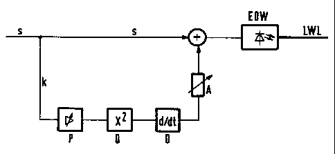
For the purpose of electric compensation of
signal distortion in an optical telecommunication system
caused by laser chirp and fiber dispersion, a correction
signal is derived from the electric transmission and/or
reception signal by squaring followed by differentiation
and added to the electric transmission signal and/or
reception signal, respectively, after necessary attenuation.


Claims

Note: Claims are shown in the official language in which they were submitted.


-8-
CLAIMS:
1. A method for electric compensation of signal
distortion in an optical telecommunication system caused by
laser chirp and fiber dispersion, characterized in that a
correction signal is derived from the electric transmission
signal by squaring followed by differentiation and is added
to the electric transmission signal after a level correction
necessary per se in the form of a signal attenuation.
2. The method for electric compensation of signal
distortion in an optical telecommunication system caused by
laser chirp and fiber dispersion, as claimed in Claim 1,
characterized in that a correction signal is derived from
the electric reception signal by squaring followed by
differentiation and is added to the electric transmission
signal after a level correction necessary per se in the form
of a signal attenuation.
3. A circuit arrangement for electric compensation of
signal distortion in an optical telecommunication system
caused by laser chirp and fiber dispersion, characterized in
that, branching from the electric transmission signal path
(s) is a correction signal path (k) which has a squaring
element (Q) and a downstream differentiating element (D) and
opens out again into the electric signal path (s) after a
downstream level correction circuit (A) via an adding input.
4. The circuit arrangement for electric compensation
of signal distortion in an optical telecommunication system
caused by laser chirp and fiber dispersion, as claimed in
Claim 3, characterized in that, branching from the electric
reception signal path (e) is a correction signal path (k)
which has a squaring element (Q) and a downstream
differentiating element (D) and opens out again into the

-9-
electric signal path (e) after a downstream level correction
circuit (A) via an adding input.
5. The circuit arrangement as claimed in Claim 3 or
4, characterized in that a level adapting circuit (P) is
connected upstream of the squaring element (Q) in the
correction signal path (k).

Description

Note: Descriptions are shown in the official language in which they were submitted.


. ,~' ~2141~6~
..
Method and circuit arrangement for electric compensation
of signal distortion caused by laser chirp and fiber
dispersion
In optical telecommunication systems with signal
transmission via optical fibers, the interaction of laser
chirp, on the one hand, and fiber dispersion, on the
other hand, leads to possibly substantial signal distor-
tion which, in particular in the case of analog signal
transmission (for example, AM-CATV) in the wavelength
window around 1.55 ~m via standard monomode fibers, can
restrict the range of such systems to a few hundred
meters.
Laser chirp, that is to say the modulation-
dependent frequency deviation of a laser, can be circum-
vented by the use of external modulators, but this
entails an appreciable outlay. An attempt can be made to
combat fiber dispersion, that is to say the wavelength-
dependent spread of the signal propagation time in the
optical fiber, by splicing in fiber pieces having a
dispersion opposite to that of the standard fiber, but it
is then necessary to accept an appreciable additional
attenuation. A further approach to a solution is offered
by electronic compensation measures; thus, an all-pass
and a low-pass filter structure (with a varactor diode)
for compensating the fiber dispersion by corresponding
signal delays are known from ELECTRONICS LETTERS
27(1991)5 dated 28.02.1991, pages 421 to 423.
By contrast, the invention adopts a different
approach for the purpose of electric compensation of
signal distortion in an optical telecommunication system
caused by laser chirp and fiber dispersion.

~1~~~6y.
~_ s ~ _
- 2 -
The invention relates to a method and a circuit
arrangement for electric compensation of signal distor-
tion caused by laser chirp and fiber dispersion. The
method is characterized in that a correction signal is
derived from the electric transmission and/or reception
signal by squaring followed by differentiation and is
added to the electric transmission signal and/or reception
signal, respectively, after a level correction necessary
per se in the form of a signal attenuation; the circuit
arrangement is characterized according to the invention
in that, branching from the electric transmission and/or
reception signal path is a correction signal path which
has a squaring element and a downstream differentiating
element and opens out again into the electric signal path
after a downstream level correction circuit via an adding
input, it being the case that in a further embodiment of
the invention a level adapting circuit can be connected
upstream of the squaring element in the correction signal
path.
The invention, which proceeds from a relationship
between the light output and the optical frequency of the
laser which is linear and phase-locked at least to a good
approximation, and is based on the finding that a signal
occurring at the end of a dispersive transmission link
essentially comprises the original signal and an inter-
ference term which can be simulated electrically in a
very simple way, is attended by the advantage that signal
distortion caused by laser chirp and fiber dispersion can
be compensated electrically at the receiving end and/or
(given a defined length of link) at the transmission end
in a very effective way independently of the mean signal
level with a very low outlay on circuitry.
The invention is explained in still further
detail with the aid of the drawings, in which
Figure 1 shows a circuit arrangement for electric com-
pensation at the transmission end, and

~~~~~s r~
..~ _
- 3 -
Figure 2 shows a circuit arrangement for electric com-
pensation at the reception end of signal dis-
tortion induced by laser chirp and fiber dis-
persion.
Represented diagrammatically in Figure 1 to an
extent required in order to understand the invention is
an exemplary embodiment of a circuit arrangement for
electric compensation of signal distortions in an optical
telecommunication system caused by laser chirp and fiber
dispersion, in which an electric transmission signal path
s leads to an optical fiber LWL via an electro-optic
transducer EOW formed by a laser diode. Branching off
from the electric transmission signal path s is a correc-
tion signal path k which has a squaring element Q and a
downstream differentiating element D and which opens out
again into the electric signal path s after a downstream
signal attenuating element A via an adding input; as may
be seen from Figure 1, a level adapting circuit P can be
connected upstream of the squaring element Q in the
correction signal path k deDendina on the tvnP of tha
squaring element.
Owing to the fact that a correction signal is
derived from the electric transmission signal by squaring
followed by differentiation and added to the electric
transmission signal after a necessary attenuation, signal
distortion caused in the optical telecommunication system
containing the optical fiber LWL by the interaction of
laser chirp and fiber dispersion is electrically compen-
sated:
The starting point is assumed to be a relation-
ship between the light output of the laser EOW and the
optical frequency thereof, which is at least approximate-
ly linear and phase-locked and can be described by means
of
~f = ~ p~t~ ~1~
wherein
Of is the frequency deviation of the laser from
the mean value given at the mean light output
poi

,
- 4 -
a is the ratio of the change in output to the
change in current of the laser,
3 is the ratio of the change in frequency to the
change in current of the laser, and
P(t) is the change in output of the laser caused by
modulation.
Owing to this (linear) relationship between light output
and optical frequency, in the case of a dispersive
optical fiber LWL the - frequency-dependent - signal
propagation time on the optical fiber depends on the
signal amplitude; if the fiber dispersion is denoted by
D and the fiber length by L, the signal propagation time
deviates from the mean value io given in the case of the
mean light output Po by
Di ~ D~LWf (2)
In the case of a change in optical output
P(t) = Pom cos(wit), (3)
caused by modulation, wherein wi/2a is the carrier fre-
quency of the ith transmission channel, the result at the
far end of the optical fiber hWL is thus a light output
of
w n
P (t-'ro)-~~ Pom~cos(wi(t-~~)) = Po'm:~cos(wit - wiDL~P(t)),t4)
wherein m is the modulation index (identical for all
signal channels). In practice, in the case of slight
interference, it holds that wi- D~ L~ ~~ P(t)cl; for example,
in the case of a standard monomode fiber it can be that
D = 1.18 10'as sa/m ( at a wavelength of 1. 55 Vim) and
L ~ 10,000 m
and in the case of a laser (Fujitsu FLD 150 F2KP)
a ~ 0.04 mW/mA and a = 550 MHz/mA,
from which it follows that D~ L~ ~ $ 1.77 10-11 s/mW.

.~ _
- 5 -
Using cos(u-v) = cos u~cos v + sin a ~ sin v
(addition theorem)
and cos v = 1 for v c 1,
cos v ~ v for v c 1
and ~cos wt = - sin wt,
-~tcos~wt ~ -2w cos wt ~ sin wt,
it is also possible to write
h w
P~(t-'~)~Pown~~cos(wit - wi~~'d = Pom~~cos wit (6)
:ail ~wi'OL~P(t)~sin wit
_ P(t)
+ wiDL~(t)~(- ~ P(t))
_ P(t) -'~iDL~ d ~~f P2~t).
instead of equation (4), when substituting equation (3)
in equation .( 4 ) .

.~ _
~~.~~~60
- 6 -
The position and intensity of the interference
term is obtained as
s'
D~~.~~ ~d~-P2(t) - ~~D~L~ ~ ~Po.m2.~~Ai. Sin(2wit)
a w
+~.~(wi+w~)~sin( (wi+w~)t) (7)
. ~s~t a=~~1
+ (w~-wi ) ~ sin( (w~-wi )t ) } .
by substituting equation (3) in equation (6).
n (n+lj/2 interference lines occur. The signal at the far
end of the optical fiber is composed of the original
signal and an interference signal orthogonal thereto.
This interference signal is proportional not only to the
optical fiber length, dispersion and chirp, but also to
the frequency at which the interference occurs.
By squaring and subsequent differentiation of the
transmission signal P(t), the correction signal is
obtained, after attenuation in accordance with the factor
- ~wiDh~, for electric compensation of the signal distor
tions caused by the interaction of laser chirp and fiber
dispersion.
Since the signal distortion term is very small
per se (approximately 40 to 60 dB below the useful signal
level), it is also possible to use the disturbed recep-
tion signal to generate the correction signal by using
squaring and subsequent differentiation to derive from
the electric reception signal a correction signal which
is added to the electric reception signal after a level

l . ~ _
correction which is necessary per se in the form of
signal attenuation.
Figure 2 represents an exemplary embodiment of a
circuit arrangement for electric compensation of signal
distortion in an optical telecommunication system caused
by laser chirp and fiber dispersion, in which an optical
fiber LWL leads to an electric reception signal path a
via an optoelectric transducer OEW. Branching from the
electric reception path a is a correction signal path k
which has a squaring element Q and a downstream differen-
tiating element D and which opens out again into the
electric signal path a after a downstream signal attenu-
ating element A; a level adapting circuit P can be
connected in turn upstream of the squaring element Q in
the correction signal path k, depending on the squaring
element used.
As follows from the above explanation of the
invention, the correction signal formed by squaring
followed by differentiation further requires a level
adaptation, specifically in principle in the form of a
signal attenuation; in the case of poor efficiency of the
squaring element and differentiating element and an
excessively low correction signal level resulting there-
from, however, a level correction in the form of a
correction signal amplification can also become necessary
on occasion.

Representative Drawing
A single figure which represents the drawing illustrating the invention.
Administrative Status

2024-08-01:As part of the Next Generation Patents (NGP) transition, the Canadian Patents Database (CPD) now contains a more detailed Event History, which replicates the Event Log of our new back-office solution.

Please note that "Inactive:" events refers to events no longer in use in our new back-office solution.

For a clearer understanding of the status of the application/patent presented on this page, the site Disclaimer , as well as the definitions for Patent , Event History , Maintenance Fee  and Payment History  should be consulted.

Event History

Description Date
Inactive: IPC expired 2013-01-01
Time Limit for Reversal Expired 2006-08-07
Letter Sent 2005-08-05
Grant by Issuance 2004-06-29
Inactive: Cover page published 2004-06-28
Inactive: Final fee received 2004-04-16
Pre-grant 2004-04-16
Notice of Allowance is Issued 2003-11-20
Letter Sent 2003-11-20
Notice of Allowance is Issued 2003-11-20
Inactive: Approved for allowance (AFA) 2003-10-23
Letter Sent 2003-09-19
Amendment Received - Voluntary Amendment 2003-08-27
Reinstatement Request Received 2003-08-27
Reinstatement Requirements Deemed Compliant for All Abandonment Reasons 2003-08-27
Inactive: Abandoned - No reply to s.30(2) Rules requisition 2003-07-07
Inactive: S.30(2) Rules - Examiner requisition 2003-03-05
Letter Sent 2000-07-13
Inactive: Status info is complete as of Log entry date 2000-07-13
Inactive: Application prosecuted on TS as of Log entry date 2000-07-13
All Requirements for Examination Determined Compliant 2000-06-29
Request for Examination Requirements Determined Compliant 2000-06-29
National Entry Requirements Determined Compliant 1995-02-03
Application Published (Open to Public Inspection) 1994-02-17

Abandonment History

Abandonment Date Reason Reinstatement Date
2003-08-27

Maintenance Fee

The last payment was received on 2003-07-21

Note : If the full payment has not been received on or before the date indicated, a further fee may be required which may be one of the following

  • the reinstatement fee;
  • the late payment fee; or
  • additional fee to reverse deemed expiry.

Patent fees are adjusted on the 1st of January every year. The amounts above are the current amounts if received by December 31 of the current year.
Please refer to the CIPO Patent Fees web page to see all current fee amounts.

Fee History

Fee Type Anniversary Year Due Date Paid Date
MF (application, 4th anniv.) - standard 04 1997-08-05 1997-07-15
MF (application, 5th anniv.) - standard 05 1998-08-05 1998-07-23
MF (application, 6th anniv.) - standard 06 1999-08-05 1999-07-23
Request for examination - standard 2000-06-29
MF (application, 7th anniv.) - standard 07 2000-08-07 2000-07-18
MF (application, 8th anniv.) - standard 08 2001-08-06 2001-07-12
MF (application, 9th anniv.) - standard 09 2002-08-05 2002-07-22
MF (application, 10th anniv.) - standard 10 2003-08-05 2003-07-21
Reinstatement 2003-08-27
Final fee - standard 2004-04-16
MF (patent, 11th anniv.) - standard 2004-08-05 2004-07-13
Owners on Record

Note: Records showing the ownership history in alphabetical order.

Current Owners on Record
SIEMENS AKTIENGESELLSCHAFT
Past Owners on Record
ERICH GOTTWALD
Past Owners that do not appear in the "Owners on Record" listing will appear in other documentation within the application.
Documents

To view selected files, please enter reCAPTCHA code :


To view images, click a link in the Document Description column. To download the documents, select one or more checkboxes in the first column and then click the "Download Selected in PDF format (Zip Archive)" or the "Download Selected as Single PDF" button.

List of published and non-published patent-specific documents on the CPD .

If you have any difficulty accessing content, you can call the Client Service Centre at 1-866-997-1936 or send them an e-mail at CIPO Client Service Centre.


Document
Description 
Date
(yyyy-mm-dd) 
Number of pages   Size of Image (KB) 
Claims 2003-08-26 2 55
Description 1994-02-16 7 257
Abstract 1994-02-16 1 14
Claims 1994-02-16 2 57
Drawings 1994-02-16 1 9
Representative drawing 2004-05-26 1 3
Drawings 1995-02-02 1 7
Abstract 1995-02-02 1 43
Reminder - Request for Examination 2000-04-05 1 117
Acknowledgement of Request for Examination 2000-07-12 1 177
Courtesy - Abandonment Letter (R30(2)) 2003-09-14 1 167
Notice of Reinstatement 2003-09-18 1 167
Commissioner's Notice - Application Found Allowable 2003-11-19 1 160
Maintenance Fee Notice 2005-10-02 1 172
Correspondence 2004-04-15 1 31
PCT 1995-02-02 4 109
PCT 1995-02-03 4 115
Fees 1996-07-22 1 80
Fees 1995-07-13 1 74
International preliminary examination report 1995-02-02 21 730