Note: Descriptions are shown in the official language in which they were submitted.
~
t
CA 02141689 2004-05-19
1
PEDESTAL MOUNT CAPACITIVE PRESSURE SENSOR
The present invention relates to a pedestal mount
capacitive pressure sensor used primarily for sensing air
pressures in air vehicle operations which is constructed to
provide long-term stability, reduce temperature-induced errors
and to provide a rugged, accurate pressure sensor assembly.
Solid-state capacitive type pressure sensors have been
well-known in the art, and are widely accepted because of their
ability to be miniaturized, and to be made using batch
fabricating techniques to hold costs down. Such prior art
sensors have used glass or semiconductor bases and formed
diaphragm layers joined together around the rim of the diaphragm
with anodic bonding, glass frit layers, metal diffusion and
similar bonding techniques.
It also has been known in the art to metalize
borosilicate glass (a type available under the trademark Pyrex,
used hereinafter) layers for forming capacitive electrodes for
use with deflecting semiconductor diaphragms. Temperature
stability is a problem for pressure sensors used in air vehicles
because they are subject to wide, quite sudden swings in
temperature. Temperature induced stresses caused by materials
which have different temperature coefficients continues to be a
problem, and stress isolation between the outer housing and the .
sensor die package is also necessary.
The present invention relates to capacitive pressure
sensors used for sensing changes in fluid pressures across a
wide range of temperatures. The temperature coefficient of the
overall sensor assembly is reduced. The capacitive sensors are
mounted on a glass tube pedestal which is secured in an outer
housing to provide isolation from both mounting and temperature
induced stresses between the metal housing and the sensor
components.
CA 02141689 2004-05-19
2
In accordance with this invention a pressure sensor
comprises a backing plate; a semiconductor-material diaphragm
having a peripheral rim and mounted on the backing plate, with
portions of the diaphragm within the peripheral rim being
deflectable relative to the backing plate under fluid pressure;
and an electrode plate for forming a capacitive-pressure sensor
in combination with the diaphragm and mounted to the diaphragm
around the peripheral rim of the diaphragm. A support mounts
the pressure sensor relative to a housing for the sensor; the
support comprising a glass tube directly supporting the backing
plate for stress isolation of the backing plate and the
electrode plate relative to the housing. A fluid-pressure inlet
passes through the support and the backing plate, to permit
fluid pressure to act on the diaphragm to deflect the diaphragm
relative to the electrode plate and cause a change in spacing
between the diaphragm and the electrode plate.
In an alternative embodiment a pressure sensor comprises
a backing plate made of a rigid material; a semiconductor-
material diaphragm mounted on the backing plate, the diaphragm
having a support rim around a periphery of the diaphragm, the
diaphragm having portions within the support rim which are
deflectable relative to the backing plate when under fluid
pressure, and the backing plate being at least two and one half
times as thick as the rim. An electrode plate forms a
capacitive-pressure sensor in combination with the diaphragm,
and is mounted to the diaphragm support rim. A housing encloses
the pressure sensor, and a glass tube is secured to a wall of
the housing and directly supports the backing plate for stress
isolation of the backing plate and electrode plate relative to
the housing. A fluid-pressure inlet passes through the wall of
the housing, the glass tube and the backing plate, to permit
fluid pressure to act on center portions of the diaphragm to
deflect the center portions of the diaphragm relative to the
CA 02141689 2004-05-19
3
electrode plate, and to cause a change in spacing between the
center portions of the diaphragm and the electrode plate.
The invention also provides a pressure sensor assembly
comprising an outer housing having a substantially rectangular
configuration with a base wall, upstanding sidewalls extending
from that base wall and a cover plate overlying the base wall. A
pressure-sensing die is sealingly mounted on the base wall and
has a pressure fitting formed to extend to the exterior of the
housing. A reference-pressure die is constructed substantially
identically to the pressure-sensing die, and is sealingly
mounted on the base wall and is oriented substantially parallel
to the pressure-sensing die. Electrical connector means
sealingly pass through one sidewall and a pair of mounting studs
are mounted on that one sidewall adjacent opposite ends thereof,
with the electrical connector means therebetween; the studs
being welded to the one sidewall for supporting the housing in a
usable position.
The sensor assembly is anchored to the housing through
bonding and brazing techniques to withstand high G-forces and
shock loads.
The sensor includes a base backing plate, a diaphragm
bonded to the backing plate around its rim and an electrode
plate overlying the diaphragm. The diaphragm and electrode
plates form a capacitive sensor which changes output as the
diaphragm deflects relative to the electrode plate.
The ratio of thickness of the base support or backing
plate relative to the diaphragm thickness and the thickness of
the electrode plate bonded to the diaphragm is selected to
assure a low temperature coefficient and provide for high
stability at widely changing temperatures. Additionally, the
thin metalization layer on the electrode plate used with the
diaphragm is formed in a manner to minimize the effect of thin
film stress relaxation over time for continued accuracy.
CA 02141689 2004-05-19
4
The housing for the pressure sensor assembly contains
two mounted sensors, one of which is active and the other of
which serves as a reference sensor. Because the two sensors are
constructed identically and mounted side by side, their
capacitive outputs, when ratioed electrically, will cancel out
common mode errors such as arising from acceleration, mechanical
stresses, thermal stresses and circuit dependent phenomena.
Illustrative specific embodiments of the invention now
will be described, with reference to the accompanying drawings
in which.
Figure 1 is a perspective view of a typical housing assembly
showing connections to the capacitive pressure sensors of the
present invention;
Figure 2 is a vertical sectional view through the housing of
Figure 1 schematically showing the positioning of an active
pressure sensor and a reference pressure sensor within the
housing;
Figure 3 is a vertical sectional view of a first form of a
typical pressure sensor used in the housing of Figures 1 and 2;
Figure 4 is a cross-sectional view of a modified pressure sensor
used in the housings of Figures 1 and 2;
Figure 5 is a view of a further modified preferred form of a
sensor used in the housings of Figures 1 and 2 taken along line
5--5 of Figure 6;
Figure 6 is a typical top plan view of the configuration of the
sensors shown in Figures 3-5;
Figure 7 is an enlarged fragmentation sectional view of the
metalized portions for the electrode shown in the sensors of
Figures 3, 4 and 5; and
Figure 8 is a schematic representation of a glass to glass
anodic bonding process.
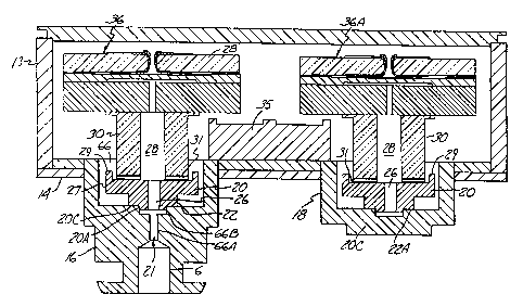
In Figure 1, a pressure sensor assembly for sensing
pressures, primarily in air vehicle installations, is shown
generally at 10 and comprises an outer housing 11, which has a
CA 02141689 2004-05-19
4a
sealed outer cover 12. A base plate 14 of the housing 11 has a
stainless steel pressure connector fitting or housing 16 for a
pressure sensing die (active pressure sensor) 36 protruding
therefrom, and sealed relative to the housing bore. A stainless
steel cap 18 for a static reference die (reference pressure
sensing die) 36A also protrudes from the base of the housing 10.
The housing base plate 14 is secured to housing sidewalls 13 by
welding or brazing. One sidewall 13 has a plurality of
electrical connections 15 sealingly passing through the
sidewall. These connectors are used for carrying signals to and
from the pressure sensing die 36 and the static reference die
36A. Also, this same wall 13 has a pair of threaded mounting
studs 17 thereon mounted near the housing 11. These studs 17
have a head 17A and can be "stud welded" or brazed to the wall
13 and provide convenient supports for mounting the sensor
housing. The connectors 15 can be accessed easily. The pressure
connections extend substantially normal, preferably 90° from the
electrical connectors 15, so access and mounting for each is
simplified. When the pressure sensing die 36 and the static
reference die 36A are sealed into the housing 11 and the cover
sealed, the housing interior chamber is evacuated and sealed so
that the sensing dies have a vacuum reference.
In Figure 2 the pressure connector 16 has an O-ring
groove so a fitting from a pneumatic line of a pitot tube can be
slipped on. The connector 16 has an interior bore 21 that
includes a shoulder formed where the bore widens out. A nickel
plated metal (preferably a nickel-iron alloy sold under the
trademark Kovar, used hereinafter) pedestal 20 is supported on
a radial shoulder surface 22. The cap 18 of the static
reference die also has an interior cavity that receives a
Kovar pedestal 20 which is supported in the bore of cap 18 on
a radial shoulder surface 22A. The cavity of cap 18 is
closed to the outside atmosphere at one end but has
internal venting to the vacuum reference inside the package to
WO 94/0988
-- 2141 ~ 8 ~ p~-/US93/08097
-5-
assure that the reference die diaphragm has zero
differential pressure. The static reference die 36A and
pressure die 36 are batch-fabricatedwørom the same wafer
stack and are identical except for the pressure fitting
and cap.
The pedestal 20 of pressure die 36 is secured
to the radial shoulder surface 22 in connector 16.
Likewise, pedestal 20 of static reference die~36A is
secured to a similar radial shoulder surface 22A in the
cap 18 .
The pedestal 20 has a through opening or bore
indicated at 26 thereto which leads to a bore 28 of a
glass (Pyres or borosilicate glass) pedestal 30 on each
of the reference and pressure sensors. Again, the
pressure die 36 will -be described, but the static
reference die 36A is identical ezcept for cap 18. A
support block 35 is also shown in Figure 2. The support
block may be used for supporting a circuit board which
provides signal processing of the capacitive outputs
from the two sensing die.
In Figure 3, pedestal 20, with annular lip 29,
is preferably made out of Rovar. The glass to Rovar
seal indicated at 31, is a tri-layer of metal on the
surface of the Pyrez pedestal 30, which includes a
bonded, deposited thin first layer of zirconium, (See
Figure 4), indicated at 32. Zirconium can be deposited
on the glass and bonds permanently to the glass. A
layer of nickel 33 is then deposited using known
techniques on the zirconium to provide a solderable or
solder wettable layer. The nickel-zirconium interface
__ is also a permanent bond. An outer coating of gold 34
is provided over the nickel layer 33 to prevent
oxidization of the nickel. The nickel plated Rovar also
SUBSTITUTE SHEET
- WO 94/05988 21 ~ I 6 8 9 PCT/US93/08097
-6-
has a tri-metal layer formed thereon prior to soldering
the metal pedestal to the glass. The tri-metal layer
may be a layer of titanium deposited::on the surface of
the pedestal 20, then a layer of nickel and then a gold
over layer. The tri-metal layer is illustrated on the
metal pedestal only in Figure 3 for convenience, but
each metal pedestal has three layers of materials
thereon where it supports and is brazed to the glass
pedestal as shown on the glass pedestal and in Figure 3.
The pressure die 36 and the static reference
die 36A are identically constructed for purposes of
having accelerations, temperature and other forces and
effects reacted identically by the two sensors to
achieve common error cancellation and thereby ensure
accurate responses across a wide temperature range and
a range of other conditions.
Referring to Figure 3, a first form of the
pressure sensor or die 36 is shown. The Pyres pedestal
indicated at 30 has a flange 38 supporting a backing
plate 40 for the pressure sensor or die 36. The backing
plate 40 is, in the fona shown in Figure 3, made of
Pyrex. A novel glass to glass anodic bond or bond
process at the interface between the surfaces of the
pedestal 30 and the backing plate 40 secures the
pressure die 36 to the pedestal 30. The anodic bond is
indicated schematically at 42. In this form of the
pressure sensor, the backing plate 40 has an opening 44
that leads from Pyrex pedestal 30 to.a pressure chamber
46 formed relative to backing plate 40 by a diaphragm 48
constructed of silicon or other suitable semiconductor.
A thin diaphragm web section 49 is formed by etching a '
cavity into one side of a silicon wafer for forming
chamber 46. The diaphragm web section 49 also is formed '
suBSrnu-rE sHEEr
211689
WO 94/05988 PCT/US93/08097
in part by a shallow recess 50 etched into the upper
surface or active face of the diaphragm. The upper
surface of the diaphragm has a doped layer 51 for
increasing its conductivity for use as a capacitive
plate, and the upper recess is enclosed with a Pyre$
glass electrode plate 52.
The Pyrex electrode plate 52 is bonded to the
rim of the silicon diaphragm, after being metalized with
a deposited metal layer indicated at 54 which has an
upper side layer 54A, and which extends along the wall
surface bounding an opening shown at 56. The opening 56
provides a reference pressure (from the sealed housing)
to the upper side of the diaphragm. The metalizing
layer 54 includes a lower section or portion 548 that is
matched in size and thickness to the upper layer 54A and
which is electrically connected to the upper layer 54A
by the metalized layer in the opening 56. The upper
layer section 54A has a lead path or tab of suitable
small size deposited on the electrode plate surface and
leading from the layer 54A. .An aluminum bonding pad is
applied to the deposited tab used for connecting a
suitable lead to layer 54. This is shown typically in
Figure 6. Also, there are two openings in the electrode
plate as shown in Figure 6 and the metalized layer has
narrower sections adjacent the openings. The cross
section through the electrode plate is to illustrate an
opening.
A lead bonding pad is also attached to doped
layer 51 adjacent to the periphery of the diaphragm and
is situated to the outer side of the electrode plate 52.
See Figure 6 for a typical showing.
In this form of the invention, the glass
pedestal axial length indicated at 62 is approximately
SUBSTITUTE SHEET
- WO 94/05988 2 I. ~ 1 ~ 8 9 P~'/US93/08097
_g_
.275 inches, and the backing layer 40 has a thickness
indicated at 63 of about 18 mils, while the diaphragm at
its rim is about 12.5 mils thick as indicated at 64, and
the electrode thickness is 18 mils as indicated at 65.
These thicknesses are selected, particularly in the
modified forms of the invention, for obtaining desired
sensor precision and long-term stability and temperature
coefficient properties over wide temperature changes.
After forming the three layers of metal on the
bottom surface of the glass pedestal, the nickel/gold
layers are soldered to the nickel plated Rovar metal
pedestal 20, whose surface has also been coated with
three metal layers in a like manner as the Pyrex
pedestal base, by use of a gold/tin eutectic solder for
a very secure mounting. A feature of the present device
is that zirconium can be used for adhesion between the -
glass and the nickel layer, which provides a solder
attachment material. Zirconium forms strong,
thermodynamically stable ozides which will remain bonded
to the glass pedestal during deposition on the soldering
of the end of the glass pedestal to metal pedestal 20.
Zirconium metalization replaces titanium, which is
commonly used for bonding metal to glass.
It should be noted that the Rovar pedestal 20
has machined surfaces Which provide for very precise
alignment with and piloting in the sections of the bore
21 of the stainless steel pressure fitting 16. As shown
in Figure 2, typically stainless steel pressure fitting
16 has a pressure bore section,66, of large diameter,
which reduces in size to a~~passageway 66A, and then
expands to a recess 66B which can be precisely machined '
on an--~insidewdiameter, so it will receive a pilot bore
SUBSTITUTE SHEET
.~ WO 94/05988 214 1 ~ g ~ PCT/US93/08097
_g_
or collar 20A of the Rovar pedestal that fits closely
within this bore 66B.
In fact, the pilot bore 20A~outside.diameter
can be machined to very precise tolerances, and a
shoulder surface 20C can be machined precisely relative
to the central bore 26. Further, the distance between
the radial shoulder surface 22 and the support surface
for the end of the metalization layer 31 can be
precisely controlled, and the surfaces can be kept
parallel to each other as well as perpendicular to the
axis of bore 21.
The cylindrical surfaces piloting the pedestal
into place and planar surfaces that are parallel to
the supporting surface in the pressure fitting 16 for
15 supporting the pedestal 20 provide a very stable, and
properly aligned pedestal 30 for supporting the pressure
die 36 and static reference pressure die 36A. Also, the
upper end of pedestal 20 has a flange 29 surrounding the
tube, the Pyrex pedestal 30 is supported within the
20 flange.
The Rovar isolator pedestal 20 forms a first
stress isolation transition piece between the relatively
high temperature coefficient of expansion of stainless
steel, as used in the fitting 16, and the much lower
temperature coefficient Pyrex pedestal tube 30. The
Pyrex tube provides further stress isolation to the
pressure dies 36 and 36A, and the Rovar fitting has an
intermediate coefficient of thermal expansion to provide
for a thermal stress transition between the two
substantially different thermal coefficient expansion
-- materials . . _
SUBSTITUTE SHEET
- WO 94/05988 21 ~ ~ ~ ~ ~ PCT/US93/08097
-10-
The Pyrex pedestal 30 also provides isolation
from stresses induced by the packaging or housing in
which the pressure sensing dies arewmounted.
While zirconium is a preferred 'metal for
applying a layer that will bond nickel (or other
suitable metal] to the Pyrex, hafnium, niobium,
tantalum, vanadium, chromium, molybdenum and tungsten
could also serve this purpose.
In the form of the invention shown in Figure
3, there is a glass-to-glass anodic bond between the
base layer 40 and the upper surface 30A of pedestal 30,
which includes a flange 38.
In Figure 4, a modified form of the invention
is shown, and includes the same glass pedestal 30 as
previously, but in this case, the upper surface 30 of
the pedestal is bonded to a silicon backing or base
plate 70 for a pressure die 71. The silicon backing
plate 70 is supported on the end of the pedestal 30
through an anodic bond. Silicon will band firmly to
Pyrex using the well-known anodic bond process. The
backing plate 70 is relatively thick (measured
perpendicular to the plane of the plate j compared to the
silicon diaphragm indicated at 72, which is directly
silicon-silicon fusion bonded to the backing plate 70-.
The diaphragm 72 has a boundary rim 73 and a thin
diaphragm Web section 74 that is recessed inward from
both surfaces of a wafer having the thickness of the
rim. The recess indicated at 75 is the larger recess
and is directly above the backing layer 70, to form a
pressure chamber 84. A very shallow recess 76 is formed
on the opposite side of the diaphragm to provide
clearance for capacitive web deflection under pressure.
A Pyrex electrode plate 78 is provided over the upper
suRssH~~
WO~ 94/05988 214 ~ ~ g g PCT/US93/08097
-11-
surface of the diaphragm 72, and is bonded to the
diaphragm at the rim 73.
The Pyrex electrode plat~:~ 78 is , made as
previously explained, and has a metali~zed layer
indicated at 80, formed as previously explained with a
top section 80A and an identically shaped and formed
lower capacitive plate section 808. Pressure ports 82
are provided in the backing layer 70 to provide pressure
to be communicated to the chamber 84 formed by the
recess 75. Reference pressure from the outer housing
acts through the opening in the electrode plate.
An aluminum bonding pad is provided on a tab
leading from the metalized layer 80 of the electrode, at
one side as previously explained and as shown in Figure
6. A bonding pad also is used for providing electrical
connection to the active surface of diaphragm 72 facing
the electrode plate, also as shown in Figure 6.
In this form of the invention, the electrode
plate 78 is also maintained at a thickness of 18 mils as
indicated at 86, and the diaphragm rim is also 12.5 mils
thick as shown at 87 and is constructed substantially
the same as that shown in Figure 3. However, the
silicon backing plate is quite thick, and is
substantially double the thickness of the Pyrex
electrode and about three times the thickness of the
diaphragm rim and as shown is in the range of 35 mils as
shown at 88. The other dimensions such as the pedestal
length would be the same as before. The outside
length and width dimensions of the backing plate 70, or
30 the glass backing plate 40 for these sensors typically
are in the range of .45 inches square. The plan view
configuration is illustrated in Figure 6.
SUBSTITUTE SHEET
WO~ 94/05988
PC'T/US93/08097
-12-
The heavy silicon backing plate 70 provides
for a reduction in the overall temperature coefficient
of the sensor. This in turn improves the performance of
the sensor when the sensor is rapidly forced to a cold
condition from high temperature ambient conditions, as
would be present when a high-performance aircraft is,
for example, departing from a desert runway and climbs
immediately into altitudes in the range of 40,000 feet
or more. Additionally, the fusion bond between the
silicon diaphragm and the silicon base plate provides a
very stable bond, with little temperature shift in view
of the fact that both parts are made of the same
materials. The fusion bond is accomplished by heating
the interfacing surfaces to a point where they actually
fuse together.
It should be noted that the silicon diaphragm
is provided with a "doped" layer on the surface facing
the Pyrex electrode, which is indicated by a heavier
line 77. The recess 76 forms a capacitive gap in a
chamber 79 with the metalized layer on the Pyrex
electrode 78. The gap spacing is in the range of eight
microns. The recesses in the diaphragm are formed
through suitable chemical etching techniques. This is
done in a.batch process. The silicon backing plate 70
is preferably P-type silicon, but N-type may be used as
understood in the art.
If P-type silicon is used, the layer 77 is
doped with boron or other suitable dopant to increase
conductivity of the diaphragm surface which is used as
a capacitive sensing surface. If the N-type is used,
phosphorus is the dopant of choice. The doping prevents
surface depletion effects which, if unmanaged, would --
cause shifts in the calibration of the sensor.
SUBSTITUTE SHEET
WO 94/05988 2 I. 4 I ~ ~ ~ PCT/US93/08097
-13-
The metalization layer on the opposing
surfaces of the Pyrex electrode in all forms of the
invention is a nickel chromium metaiization, that is
presently done in the art for forming resistors on glass
or Pyrex layers.
The ratio of the thickness of the silicon
backing plate to the thickness of the diaphragm is at
least two and one half to one and the ratio of thickness
of the silicon backing plate to the electrode plate is
about two to one. The thick backing plate aids in
temperature stability when the backing plate is made of
the same material as the diaphragm so they can be fused
together, with no layer of frit or bonding material
between them. The Pyrex electrode plate is also
substantially thinner than the backing plate.
. The entire sensor 71 is made without the need
for frits or other bonding agents.
In Figure 5, a further modified form of the
pressure die ( and also reference die ) is disclosed. The
form of the sensor of Figure 5 is most preferred, by
providing greater temperature stability and using a
predetermined diaphragm rim thickness relative to the
diaphragm deflecting web thickness, as well as the
additional benefits of reducing the thickness of the
electrode plate.
In the form of the invention of Figure 5, the
Pyrex pedestal 30, which is the same as previously
described, is anodically bonded to a thick silicon
backing plate 90 of a pressure sensor or die 89, which
has a pressure passage 91 in the center. The silicon
backing plate 90 is in turn fusion bonded to_a silicon
diaphragm 92 around a diaphragm rim portion 93. The
diaphragm has a thinner web section 95. The diaphragm
SUBSTITUTE SHEET
WO 94/05988 2 I 41 a ~ ~ p~/US93/08D97
-14-
web section 95 has a desired thickness and is formed by
etching a pressure chamber recess 97, and a capacitive
sensing chamber recess 99. The surfaa,e of the diaphragm
web facing away from the silicon backing plate 90 has a
doped layer 101 thereon, for increasing conductivity,
and an aluminum bonding pad 103 (Figure 6) is connected
to this doped layer outside the periphery of the Pyrex
electrode 104. The Pyrex electrode 104 has a metaiized
layer 105 that is formed as described in connection with
Figure 3, and is metalized through one or more provided
openings (two openings as shown in Figure 6), so that
the metalized layer has two substantially symmetrical
sections 105A, arid 105B. The layer 105B is a sensing
layer forming a capacitive plate that faces the doped
layer 101 on the diaphragm 92. If desired, the openings
in the glass electrodes can be sealed or eliminated to
provide an internal vacuum in the chamber below
electrode plate 104.
In Figure 6 a bonding pad 107 bonded to the
metalized layer 105 is shown provided at the edge of the
Pyrez layer as well. A tab of metal is formed on that
layer for the bonding pad 107.
Referring back to Figure 5, in this form of
the invention, the diaphragm support edge or rim 93 has
been reduced in thickness. It is specifically desired
to be a function of the thickness of the center
diaphragm or web section 95 correlated to the depth of
the etch forming the capacitive sensing recess or
chamber 99. The thickness of rim 93 is formed to be the
thickness of the central web portion 95 of the diaphragm
plus two times the depth of etch of the capacitive.
sensing chamber 99, Whichyis preferably eight microns
deep. Thus, the diaphragm rim thickness indicated at
SUBSTITUTE SHEET
W0~94/05988 ~ ~ ~ ~ ~ ~ ~ PCT/US93/08097
-I5-
110 is the central web thickness plus 16 microns, or in
this instance a 6.5 mil thickness.
The thickness of the Pyre$~electrode_has been
reduced to 12 mils, as indicated by the dimension 112,
and the thickness of the silicon backing plate has been
increased to 50 mils, as indicated by the dimension 114.
All of the parts are bonded together, either
by anodic bonds where Pyre$ to silicon junctions are
made, or by fusion bonding for the silicon-to-silicon
interface between the diaphragm and the backing plate,
to eliminate any need for material that may cause
thermal instability, such as glass frits.
By finite e'~ement modeling,. it has been
established that the temperature coefficient has been
reduced, and is actually about half of the sensor
illustrated in Figure 4, and about a fourth of the
temperature coefficient of the device shown in Figure 3.
By having the Pyrex glass electrode plate in
the range of one-fourth of the thickness of the backing
plate 90, and the diaphragm rim in the range of one-half
of the thickness of the glass electrode based on the
thickness of diaphragm web section 95 and the depth of
capacitive chamber 99, a very temperature stable sensor
results.
When the sensor of Figure 5 is assembled as
shown in Figure 2, and a static reference die
constructed in this manner is also used as shown at 368,
very stable performance is achieved. In the overall
package, additional steps are taken to ensure adequate
long-term stability. One improvement that is used with
the present invention is to minimize the effect of thin-
film stress relaxation over time in relation to the thin
SUgST(TUTE SHEET
_.'VO 94/05988 PCT/US93/08097
214168
-16-
nickel chromium metalized layer placed on the Pyrex
electrode plate.
Figure 6 is a representation of the typical
plan view of one of the miniature sensors utilized in
the present invention, and is specifically a plan view
of Figure 5. The metalized layer 105A is shown on the
top. It has a larger center portion and~narrower end
portions, as shown. The end portions have the pressure
openings therein as shown, the openings 105C. The
passages or openings 105C are also shown. A short tab
107A is formed on one edge of the metal layer 105 with
the aluminum bonding pad 107 thereon. The metal layer
section 105A is formed to be identical in size and
shape, and in registry on both the top and bottom of the
Pyres electrode plate as shown in an enlarged view in
Figure 7. The metal depositing pattern is identical on
the top and the bottom of electrode plate 104, except
for the small tab for the aluminum bonding pad 107. By
replicating the metal pattern from one side of the Pyrex
electrode plate onto the other side, the thin-film
stresses cancel, provided they are deposited under
nearly identical conditions and are of the same
thickness. The metal deposition is carefully carried
out in the process, so that the metalized layers on each ~-
of the electrode plates 104 is the same on the top and
bottom. This can be done at the wafer level during the
batch fabrication process by suitable masking and using
identical deposition techniques on opposite sides of a
large Pyrex wafer from which the electrode plates are
made. In this way, several electrode plates may be
formed on a wafer for later separating into the
individual pressure-sensing dies.
SUBSTtTtlTE SHEET
~14~68~
WO 94/05988 PCT/US93/08097
-17-
The stress-compensating features of having the
metalized layers on the opposite sides of the glass
electrode plate reduces effects which are caused by
differences between the coefficient of thermal expansion
of the metalization layer and the Pyrex glass . In other
words, the stress from different temperature
coefficients will be balanced on opposite sides of the
Pyrex electrode plate. The electrode plate will not be
caused to bow or deform due to the metalization from its
reference position because of metalization on only one
side.
In this invention the diaphragms of the
pressure sensing die and the reference die are etched on
the same silicon wafer, at the same time, and next to
each other in all steps of the processing so that when
the diaphragm wafer is bonded to the electrode and the
backing wafers, adjacent die will react identically to
temperature and other environmental conditions. When
separated from the wafer, adjacent die are kept in pairs
and mounted into the sensor package, one becoming a
pressure sensing die, the other a reference die.
A highly stable pressure sensing die is
provided, utilizing the principles of having a rigid
base plate and selecting the preferred ratios of
diaphragm thickness and thickness of the overlying glass
electrode utilized, to minimize temperature effects.
As shown in Figure 8, a procedure for
anodically bonding Pyrex glass to Pyrex glass is
presented. This is used in the sensor of Figure 3 for
bonding the base layer to the glass pedestal.
In Figure 8, schematically, there is shown a
Pyrex layer 150 and a second Pyrex layer 151 that are
going to be anodically bonded together. on the surface
SUBSTITUTE SHEET
WO 94/05988
1 j~ ~ ~ g ~ PCT/US93/08U9~
-18-
of one of the Pyrex layers or wafers, a layer of
titanium that is approximately 375 thick (preferably
kept within + or - 50~) is deposited and oxidized in air
to forth titanium dioxide (Ti02). Subsequently, a layer
of Si3N4 that is approximately 3200 (preferably kept
within + or - 2500 thick is plasma deposited at a
temperature that is as close to the bonding temperature
as possible. These layers form an ion barrier on the
Pyrex wafer 151 and are shown at 153. The other Pyrex
layer, 150, which is shown at the top layer is then
placed in contact with the layer of Ti02 and Si3N4, and
these two layers are set on top of a gold foil layer
shown schematically at 156. Alternatively, 250 of gold
can be deposited on the side opposite layers 153 to
replace the gold foil. The two wafer stack is then set
on top of a hotplate ar heater that can reach
temperatures in the range of 375°C. This heater is
shown at 158.
The hotplate 158, with the parts resting
together and stacked as seen in the exploded view of
Figure 8, is romped up to a peak temperature of
approximately 375°C. When the temperature of the
hotplate reaches 250°C and thereafter, a voltage of
about 800 volts is applied across the wafer stack with
the polarities as shown in the drawings. The positive
polarity is connected to the gold foil side 156 and the
negative polarity is attached to the upper layer 150.
As the voltage is applied, a hermetic seal begins to
take place between the. two wafers, 150 and 151, reaching
completion in about 15 minutes.
The principal of operation is that Ti02 and
Si3N4 layers serve as a barrier to positive alkaline
ions which can flow up towards the cathode from the
SUBSTITUTE SHEET
'- W0~94/05988
- PCT/US93/08097
-19-
bottom Pyrex wafer 151. This allows the formation of a
depletion layer at the bottom surface of the top wafer.
Layers other than Ti02 and Si3N4,~::which can block
alkaline ions also could be used. The gd~ld foil or
deposited gold film prevents bonding from taking place
at the bottom surface. The bonding mechanism at the
Pyrex and Ti02/Si3N4 interface is - then similar to the
well documented silicon-Pyrex anodic bonding process.
While the most preferred thicknesses of layers
and other parameters are listed above, the Ti02 layer is
based on a deposited titanium layer that ranges between
about 250 and 500. After deposition, the titanium is
oxidized and.the layer will grow. The Si3N4 layer can
be between 2000A and 40001. Bonding temperatures in the
I5 range between about 250°C and about 500°C are useful.
Voltages ranging between 500 and 1000 VDC can be used.
The temperature for plasma depositing the Si3N4 is as
close to the bonding temperature used as possible.
The glass-glass anodic bond process will work
on borosilicate glass or other type of glass having
alkali ion glass modifier.
Although the present invention has been
described with reference to preferred embodiments,
workers skilled in the art will recognize that changes
may be made in form and detail without departing from
the spirit and scope of the invention.
SUBSTITUTE SHEET