Note: Descriptions are shown in the official language in which they were submitted.
d . .
~ WO94~0612~ 2 ~ 5 ~ PCT/US~3/08232 .
s
COINCIDENT ACTIVATION OF PASS TRANSISTC)RS
IN A F~ANDOM ACCESS MEMORY
Field of the lnvention
This invention relates to semiconductor
memory devices and more particularly to high speed,
high density, low power random access memories.
s ~ ~ Backqround~of the Invention
Read/write:memories, al50 referred to as
Random Ac~ess Memories (R~) are widely used to store
:~ programs and data for~microproGessors and other
electronic devicesO The avai;l~ability o~ high speed,
10 ~high density and low power RAM~devices has played a
cr~cial role in the price reduction of personal
compu~ers and in~the integration of computer technology
into ~onsumer electronic devices.
A typia~l RAM:i~n~lud&s a:large number of
;;1;5; memory:ce11s~arranged~in~an array of rows and columns~ j
Eaoh memory~:~cell is;typically capable of storing
therein a binary digi~ e. a binary ONE or a binary
';'ZERO. ~:Ea~Ch row of ~he~;memaxy cell array is typically
connected ~o a word line and each column of ~he memory
20 :cell:array is typicaIly connected to a pair of bit
lines.~Read and write;operations are performed on an
individual cell in the memory by addressing the
appropri~ate row of the array using the word lines and
addressing the appropriate cell 1n the addressed row
WO94~06120 2 ~ P~T/US93/08232
using the bit lines. ~epending upon ~he signals
applied to the bit lines, a write operation may be
performed for storing ~inary data in the RAM or a read
operation may be performed for accessing binary data
which is stored in the RAM. When read and write
operations are not being performed, the RAM is
typically placed in an idle operation for maintaining
the binary data stored therein.
RAMs are typically divided into two general
classes, depending upon the need to refresh the data
stored in the RAM during the idle state. In
particular, i:n a Dynamic Random Access Memory (DRAM),
he data stored in th~ memory is lost unless the memory
is periodically refreshe~ during the idle operation.
In contras~, in a Static Random Access Memory (SRAM~
there is no need to refresh the data during an idle
operation, because the data stored therein is
maintained as long as electrical power is supplied to
the SRAM. In the present state of the art, it is
generally poss:ible to fabricate higher density DRAM
arrays than SR~M arrays because the individual memory
ells of a DRAM include fewer transistors ~han the
indivldual cells of an SRAM.~Howe~er, SRAMs tend to
operate at higher spe~ds than DRAMs, because there is
; 25 no::need:~o~ refresh the data ~tored therein.
Accordingly,~both SRAM5 and:DR~Ms~are typically used in
,
computer systems, with the~SRAMs ~eing used for high
sp~ed memory (of~en referred to as "cache" memory~,
~ whi~le~the DRAM is typically used for lower speed, lower
- ~ 30 cost mass memory.
Three general design criteria govern the
performance of random acceiss~memories. They are
density:, speed and power dissipation. Density
describes the numher of memory cells that can be formed
on a gi~en integrated c1rcuit chip. In general, as
more cells are fabricated on a Very Large Scale
.
~.:
WO94/06120 2 ~ G ~ PCT/US93/08232
~3~
Integration (VLSI) chip, cost is reduced and speed is
increased.
The performance of random access memories is
I also limited by t~e power consumption thereof. As
power consumpticn increases, more sophisticated
packaging is necessary to allow the integrated circuit
to dissipate th high power. Moreover, high power
circuits re~uire expensive power supplies, and limit
applicabili~y to portable or ba~tery powered devices.
, 10 Finally, speed is also an important
consideration in the operation of a random access
memory because the time it takes to reliably access
~; data from the memory and write data into the memory is
an important parameter in the overall system speed. It
will be u~der tood by those having skill in the art
that the parameters of speed, density and power
:~: dissipation are generally interrelated, with
improvements in one area generally requiring tradeoffs
~; in one or more of the other areas.
A typical SR~M cell is a six transistor cell.
Four of the transistors form a pair of complementary
inverte:rs each of whlch includes ~ input and an
output, with the input of the first complementary
inverte~ being connected to the output of the second
complementary inverter and the input of the second
complementary inverter being connected to th~ output of
th~ first compl~mentary inverter. The pair of cross
~ coupled inverters form~ a latch for storing a binary
.~ digit ~herein as long as power is a~plied to the latch.
The fifth and sixth transistors are a pair of "pass
transist`ors" which provide external access to the
~; memory cell for reading and writing operations.
: Typically,:the co~trolled electrodes, (for example the
sour~e and drain electrodes) of the first pass
transistor are serially connected between one of the
associated bit lines and the output of the first
complementary inverter, and the controlled electrodes
,
W094/06l20 21~18~0 4 PCT/US93/08232 ~ ~
of the second pass transistor are connected between the
other associated bit lin~ and the output of the second
complementary inverter. The controlling electrodes
(for example gate elec~rodes) of both pass transistors
are connected to the associated word line. Thus, the
pass transistors of all SR~ cells in a row of the
array are connected to the associat.ed word line, and
the pass transistors of all SRAM cells in a colu~n of
the array are connected to the associated pair of bit
lines~
In operation, when a word line is selected,
one of the pass ~ransistors in each of the cells in the
selected row sink curr~nt from the associated bit line.
The pass transistor in the c~ll which sinks the current
will be dependent on the digital sta~e of the RAM cell,
but one pass transistor in each cell will sink current.
After the word line is deselected, all of the bit lines
are recharged up to a xeference voltage~ ~ypically the
: power ~upply volta:ge VDD-
` 20 ~n~ortunately, the above described current
sinking and bit Iine recharging in each cell connected
~; ; to a selected~word line consumes ~ excessive amount of
¦~ power during read and write operations. For example,
jl : assume there are 256 columns in an S~M array, so that
: : 25 256 pass transl tor pairs are connected to each row.
the sink current for each pass transistor pair is
lmA, then 256mA is ~rawn upon selection of a word line
: a~d another 256m~ is drawn upon deselection of the word
line. Although this power:drain is a transitory power
drain, which only occurs during selection and
' deselection o~ a word line, it nonetheless effects the
:; transient power consumption of the SRAM.
: Attempts ha~e~been made to decrease the
~: transient power consumed during a word sele t/deselect
3S operation by~dividing the SRA~ array into a plurality
of smaller arrays, thus reducing the number of pass
transistor pairs connected to any single word line.
~ !
. 0. ~....... ~0.~...... ~...... 21I~Q~r
. . O . O . ~,0 s ~ . . . s ~
--5--
~nfortuna~ly, word decodin5 tlme incr-ases when the
array is divided- The pnysical size of t:ne array also
increases, resulting in a decrease in density.
; Additional aadress line ca~acitance is also incroducsd,
thereby incr~asing the powe- dissipation to the array,
and a corres?onding loss in spe~d. ......
U.S. Patent 3,529,612 to Har~ert entitled
Operation of Fleld ~frect Transistor Circuit Having
Substantlal Distributed Capacitance describes two pairs .-~
1~ of pass transistors which are serially connected betwe~n - -
~word lines and bit lines and a memory cell for
maintai~ing the d:lstrlbuted capacitance at a Lixed value : :
~ ' during the major portion of the memory o~erating time.
U~S. Patent 3,63~,202 to Schroeder entitled ~ccess r
15 Circuit ArrangemeIlt for E~ualized Loading in Integrat~d
Circuit Arrays descri~es a similar arrangement of two
pairs o~ serial pass transistors for a memory.
u.S. Pat_nt 3,893,087 to Baker e~titl~d ~a~aom
ACCGSS Me~rnory hTi th Shared CQ1UIrU~ Conductors aescribes a
random access memory which lncludes a single c~lumn lire
which ls shared by ad~acent columns o~ memory cells.
; European Patent~Application 0 179 ~51 A2 to Wada et al.
entitled Se.~iconductor Memory Device describes an address
transitio~ detection system ~or a semiconductor mémory
: ~ :
dev}ce which includes CMOS inverters as a part therecr.
Summarv of the lnvention
It is thererore an object of the present
invention to provide an im~rove~ random acc-ss memor-
~` 30 ~cell and an lmproved~random access memory uslng same
It is another object of the inven~icn ~o
provide a memory array which consumes less ~cwer than
con~entional arra~s during word line
selectlon/ceselectlon.
t is ye~ another object of the inventlon to
provide a high density, hich speed, low transi_nt power
random access~me~ory design.
~ ~ .
ENDED S~EET
;~:: : ::
-5/1-
These and other oDjects are provi~ed accordins
to the ~resent invention by activating the pass
ans;stors in a random access memory (R~) cell only
u~on coincident ~simultaneous) selection of both the
S assoc~at~d row and the associated column o the memo~y
cell, ana preventing activation of the pass transi.stors ~ 0
in a memory cell otherwise. Coincident ~ass transistor
activation means is pro~ided for activating only those . .
pass transistors in memory cells which are at an
10~ intersection:of a selected row and a selected column, ard 0
or preve:nting activation of the pass transistors ln
~ memory cells which are not at an intersection o a
selected row and a selected column o the array of memory ..
~; ~ cells. In a con~entional: RAM in which only one cell ln
~; raY is read cr e - the memor cells
at any siven time, w th the pass transistors in the .
f~ is selected, only
~ ~ :
:~ ; 9
~;;' ~ : ,.
f
A~ltNOC~sHcET
W094~06120 2 1 ~ 1 8 ~ ~ PC~/US93tO8232 - ~i
-6-
the pass transistors in the memory cell coupled to the
simultaneously selected bit line are active, rather
than all of the pass transistor pairs connected to the
word line being active. ~ccordingly, in a RAM array
having 256 columns of cells, transient power
consumption during word line sele~tion and deselection
is reduced by a factor of 2~5. Subdivision of the
array, with the resulting loss of density and speed, is
not required.
Coincident pass transistor activation
according to the present invention may be obtained by
providing a column select line for each column of the
memory array. Word:decoders and column decoders
simultaneously select at least one of the plurality of
word lines and at least one of the plurality of column
select lines. Each cell also~includes gating means,
: which is electrically connected to at least one of the
associated column select line, the associated word line
and the associated pass transistors. The gating means
electrically activates the associated pass transistors
only upon simultaneous selection of the associated
column selèct line and the associa~ed word line, and
:prevents activation of the associated pass transistors
otherwise.
; 25 The gating means in each memory cell may be
implemented in many ways. Preferably, the gating means
is a third complementary transistor~inverter which is
connected between one o~ the associated row sel~ct line
: or column select line, and a reference ~oltage such as
ground. Thus, each cell is preferably an eight
ransistor céll; ~our transistors for the latch, two
pass transistors and two transistors for the-gating
means. The output of the third complementary inverter
is connec~ed to ~he con~rolling elP-ctrodes (for example
gates~ of the pair of pass transistors. The input of
he third inverter is connected to the other of the
column select line or row select line. Thus~ when a
2~41~
, , ~094/06120 PCT/US93/08232
--7--
row is sel~c~ed, the pass transistors are not activated
unless the associated column is also sele~ted.
! Accordingly, the gating means provides a logical ~ND
¦ function, in which the pass transis~ors are activated-
only upon selection of the word line and column select
line of the cell. In an alternate embodiment of the
gating means, the complementary inverter may be
replaced by a single transistor and resistor serially
connected between the word line and a reference
voltage.
In yet another embodiment of the gating means
of the present invention, each cell is provided with a
seventh and eighth transistor. The controlled
~ electrodes (for example source and drain) of the first
pass transistor and the seventh ~ransistor are serially
connected between the associated bit line and the
:;~ output of the first complementary inverter. The
~: co~trolled electrodes of the second pass transistor and
the eighth transistor are serially connected bPtween
the associated bit line and ~he output of the second
. : complementary:inverter. The controlling (for example
gate) electrode of one of the first pass transistor and J~
the seventh transistor is connected to the word line,
: ~ and the controlling electrodes of the other of the
~irst pass transistor and the seventh transistor is
connected to the associated column select line. The
;:~ controlling ~ilectrode of one of the second pass
transistor and the eighth transistor is connected to !~
: the associated word line and the controlling ele~trode -~
of the other o~ the second pass transistor and the
eighth transistor i5 ~connected to the associated column
select line. Accordingly, the pass ~ransist~rs are not
: acti~ated unless the seventh and eighth transistors are
activated by selection of the associated bit lineO
As describe~ above, a R~M cell according to
the present invention will preferably use eight
transistors rather than the six transistors typically ,,
;
.~
i WO94/06120 21~18~ PCT/US93/0823~ ~ ~
1 -8-
~ used. However, in the preferred embodiment the
3 additional transistors are minimum geometry transistors
so that the size of the individual cells dses not
j~ increase appreclably. ~oreover, three unexpected
;3 5 advantages aris~ as a result of the use of the
Ji coincident selection means of the present invention: 1
increased speed due to reduced capacitance; (2)
increased manufacturing yields; and (3) the ability to
~,1 share blt lines.
Decreased capacitance is present because
.~ during a row select operation only diffusion
~ capacitance of the gating means per column loads the
.1 word line, rather than gate capacitance of the two pass
transi~tors per column. The loading capacitance on the
15 word line driver is thus decreased significantly,
resulting in faster operation. Increased manufacturing
: yields may be obtained because the memory only selects
cells at the intersection of a selected row and column.
Thus, it is easier to provide redundant cells to
20 replace defective cells because the word driver need
~ not address all celIs in a row. Increased
::~ manu~acturing yields may therefore~be expected.
: ~
The third unexpected advantage of th~ -
: coincident selection means of the present invention is
~: 25 the ability of the memory columns to share adjacent bit
; lines. In particular, in the conventional RAM
architecture described above, each column includes a
pair of bit lines which are used for column addressing
as well as data reading and writing. ~owever, since
30 the coincident selecti~n means of the present invention
includes a column select line for each column of the
array, a shared bit line may be used between adjacent
columns of cells, since only one of the columns will be
selected by the coIumn:select line.
3S In a conventional RAM architec~ure, shared
bit lines would create erroneous operation. However,
~ when the coincident selection means of the present
!1 ~
o o ~ ~ ..
o ~ e ~ U
~? ~ o 9 ~ ~ o ~ ~ ~ .
! - J ~ O ~ ~0 ~ O ~ ~ ~ ' 6~
O ~ ,, . " ~ , .
O ~ O ~ o ~ ~ o o
g_
invention is used, snared ~it lines arQ possible.
Accordingly, the SR~ of the presert invention preferably
includes a single bit li~e ~etweQn each pair o adjacent
columns of memory cells for transl~erring binary cata to ,,
5 and from the memory cells, wich the memory cel~s in each
air of adjacent columns being connected to the bit line ~-oo-
cherebetween- A high density memory design is therefore
provided. 7
The coincident selection means of the present ,-~ -
10 invention including shared bit lines may be used in any ~-
~M design. ~owever, the coincident selection and shared
it lines of the present invention are prererably used : :
~ with the Dif_erential Latching Inverter (DLI) o,~ U.S. - -
Patent ~os. 5,304,874 and 5,305,259 both entitled ~. .
lS Di rferential La tching Inverter and Random Access Memcry
Using Same, hereinafter referred to as the "~arent
Applications". As desc_ibed in the Parent Applications, ..
the DiLIer-ntial Latchi~g Inverter (DLI) is responsive to :-
the volta~e on a pair G-- diLf2rential inputs thereto.
The DiLre~ential LatchinG Inverter (DLI) may be connected
;~ to a pair of bit lines in a memory array, for sensing the
binary state of the state of a selec~ed memory cell.
When one of the-input signals to the DLI rise above a
predetermln2d threshold, the DLI is responsive to a small
differentlal component between the signals applied
thereto to rapidly latch the output of the inverter to
one logical state or another. For example, in a memory
using five volt and ground ref2rence voltages, when an
i~put signal to the DLI is above one volt, and an input
di iLerential ' of at least two millivolts is ~resent
e~wee~ the in~ut signals, the DLI rapidly latches up to
a first or a second logical value depending u~on which o
the inputs has the higher input diffPrential.
The Di-ferential Latching Inverter of the
?a~ent Appl t cations~ may be implemented using a mlnimal
t
h~ N~ED SHEET
i
1,
'~, W094/0~20 2 ~ 41~ fi ~ P~r/uss3/os232 ~
-10-j
number of field effect transistors, as described below,
~ and does not require the generation of a separate
;~ reference voltage or require high gain analog linear
sense amplifiers ~or operation. Accordingly, high
speed, low power, high density sensing of signals
stored in a random access memory is provided.
A basic design of a Differential Latching
~: Inverter of the Parent ~pplications includes a pair of
complementary field effe t ~ransistor inverters, each
of which is connected between first and second
: reference voltages, typically the power supply voltage
~DD and ground, with each inverter including an input
and an outputO ~ccQrding to the Paren~ Applications,
~he F~Ts of each of the first and second co~plementary
~;~ 15 inverters are designed to producs an inverter transfer
function which is skewed toward one of the first or
econd reference voltages. ~n other words, the
inverters do not produce a symmetrical inv~rter
transfer function relative to the first and second
réference volt~gPs . Rather, the transfer function is
skewed toward one of the~re~erence voltages. In a
~ preferred~embodiment,:the voltage ~ransfer function is
`~ skewed towards ground by a ~actor o~ 2~ less than a
`~ symmetrical inve~ter, so~ tha~ a voltage thr~shold of
2S abo~t one volt causes tha inverter ~o rapidly change
.~ state,~;upon sensing a voltage differential of about two
: millivolts.
The:first and second skewed inverters of the
Parent Applications are cross coupled ~y connecting the
inpu~ :o~ the first inverter to the output of tha second
;~ inverter ànd the input of the second inverter to the
ou~put of the first inverter, to thereby create a
latch. A ~irst bit line is connected to the input of
the first inverter and a~second bit line is connected
; 35 to the inpu~ of the second Lnverter ~
The ~if~erential Latching Inverter (DLI) of
the Parent Applications exhibits three stat~s. When
:J~
~,WO94/06120 2 ~ a~ PCT/US93/08~3
one or the other input to the DLI rises above the
threshold voltage and an input differential of two
. millivolt or greater is found between ~he two bit line
inputs, the DLI latches to a binary ONE or binary ZERO
state. In a third or reset state, in which the bit
line inputs thereto are both below the D~I's threshold
voltage, both outputs o~ the DLI are ZERO. No DC power
j is dissipated by the DLI in either of its three ~table
states, and minimal power is dissipated by the DLI when
10 it switches from one state to another.
The skewed transfer function, first and
s~cond complementary inverters of the DLI may be
produced by controlling the dimensions of the
cs~plementary FET transis~ors of the skewed inverters
15 so that the product of the square channel saturation
current and the ratio of channel width to length of the
FETs of a first conductivity type is substantially
greater than the product of the square channel
saturatiQn current and the ratio of the channel width
20 to length of the FETs of the second conductivity type~
Preferably, the products of the square channel
saturation current and the ratio o~ channel width to
length ~if~er~by a factor of ten.
; : In a particular embodiment of the DLI, a pair
25 of pull-up FET~ may also be provided, with the
controlled electrodes (source and drain) of a firs~
pull up FET being connect~ between the first reference
voltage and the output: of the first complementary FET 5
inverter, and the controlled electrodes of a second
30 pull-up FET being conn~cted batween the first reference
voItage and the output of the second complementary FET
inv~rter. The controlling electrode (g~te) ~f the
~:~ first pull-up:FET is connected to the output of the
~: secon~ complementa~y FET inverter and the controlling
:~ 3~ electrod~ of the second pull-up FET is connected to the
output of the first complementary FET~inVerter. These 7
.
.
WO94/~120 2 ~ ~ 1 8 6 ~ PCT/US93/08232 ~ ~
-12-
cross coupled pull-up FETs increase the latching speed
of the DLI.
The output of the first and second
complementary inverters may be coupled to a third and a
fourth complementary FET inverter, respectively. The
third and fourth inverters produce an inverter voltage
transfer ~unction which ~s symmetrical be~ween the
first and secund reference voltages. The outputs of
the differential latching inverker are the outputs of
the third and fourth complementary FET inverters.
The DLI may also include a second pull up
circuit, which is connected to the outputs of the first
an~ second skewed transfer function inverters, for
rapidly pulling the outputs of the firs~ and second
inverters to the first reference voltage (VDD), and
thereby pulling the outputs of the third and fourth
~ symmetrIcal transfer function inverters to the second
:~; reference voltage~ (ground) in response to an input
signal applied thereto. The input signal is applied
;~ 20 immediately upon a successful data read, or immediately
upon verification of a success~ul data write, to
rapidly bring the ~LI ~o the third~(reset) state and
prepare the DLI for a next read or write operation.
External clock timing is not requ red. Rather, the
reset set is initiated internally, upon completion of a
~ ~ read or write operation.
:;: The Differential Latching Inverter of the
Parent Applications may b~ used in high speed, high
density, low power random access memory architecture as
follows. An array of memory cells is arranged in a
plurality of rows and~columns,~with a word line
conneoted to each row and a pair of primary ~it lines
connect~ad to each colum~. Signal bit lines are ~;1
: provided, orthogonal to the primary bit lines, and a
respectiv~ pair of signal bi~ lines is connected to at
least o~e respec~ive pair of the primary bit lines at
`~ 21~1~6-~ ~
.WO~4/06120 - PCT/~'S93/08232-
-13-
one end of the primary bit lines. A DLI is connected
between each pair of signal bit lines.
. The primary bit lines are coupled to a first
~,; reference voltage, typically power supply voltage VDD~ ',
31 5 during the idle operation, an~ a selected one of the
primary bit line pairs is decoupled from the first
reference voltage during a write operation. The signal
bit lines are coupled to a second reference voltage,
` preferably ground, during an idle operation and are
: lO decoupled from the second voltage during a read or
write operation. The primary bit lines and the signal
bit lines are coupled together during read and write
3 operations and decoupled from one another during an
idle operation.
The primary bit lines may ~e coupled to the
first reference voltage using a first coupling means.
The signal bit lines may be coupled to a second
reference voltage using a second coupling means, and
the primary bit lines and the signal bit lines may be
20 coupled togPther Using a third coupling means. In one ,~
embodiment, the third coupling means is loated at the
one end of the primary bit lines,~adjacent the signal
:~` bit lines, and the first coupling means is located at
the opposite end of th~ primary bit lines t distant from
the signal bit lines.
,~
It:has been found, according to the Parent
Applicatlons, that improved results are obtained when
. both the first and the third coupling means are located
a~ the;one end~of the primary bit lines, adjac~nt the
signal bit lines. The ~oltage drop due to the
~i .
resistan;~e of the primary bit lines is eliminated, and
!~ the speed of the random access memory is increased. In
this configuration, the primary bit lines operate as
unterminated transmission linesr Feed~ack between the
signal bit lines and either the firs~ coupling means or
the second coupling means, or both, may also b~
provided to further increase speed.
.
.. . .. .. , i
WO94/06120 PCT/US93/~8232
21 il~60
Accordingly, during an idle operation each of
the primary bit line pairs is referenced to VDD and each
of the signal bit line pairs is referenced to ground.
All of the DLIs are in their third or rPset state. In
order to read, thP. signal bit lines are decoupled from
the second voltage reference source (ground) and the
primary bit lines remain coupled to the first voltage
reference source ~VDD)~ A word decoder selects a given
row. A bit decoder couples a primary bit line pair in
:~ 10 a sPlected column to its associated signal bit line
pair. The amount of voltage delivered to one bit line
or the other of the sel~cted primary bit line pair
drops more rapidly than the other due to the current
conducted by one of thG memory cell pass transistors,
~, 15 as controlled by the state of the selected m~mory cell
being read. This current differential translates to a
voltage differential on one:or the other of the signal
bit lines of the associated signal bit line pair. When
the voltage differential on one of the signal bit lines
exceeds the ~LI's threshold voltage, the DLI will
rapldly latch into one or the other state depending on
the signal bit line which had the~higher voltage.
Accoxdingly, high speed sensing of data read from a
random access memory is:provided with minimal
supporting circuitry.
The outputs of all of the DLIs may be
directly connected to a pair o~ OR gates, with the
output of one OR gat~ signifying that a logical ONE has
been rea~ and the outpu~ of ~he second OR yate ',
: 30 signifying ~hat a logical ZERO has been read.
Connection of all of the DL~s to a single OR gate for
reading is possible because all of the DLIs which are
not being read are in their third or reset state with
bo~h outputs thereof at ground potential. The output
of the activated DLI may be placed in a read register
; and provided as the memory output. Once a DLI has been
latched and the data has been read, the memory is
2 1 ~
WO94/06120 PCT/U593~08232
15-
I rapidly restored to the idle state by pulling the
active DLI back to its idle stateO The signal bit
lines are recoupled to ground, t~e primary bit lines
. remain coupled to VDD and the signal bit lines and
primary bit lines are decoupled from one another.
~ Accordingly, a self-timing operation is provided.
I In a write operation, a word decoder selects
I a given row, a selected pair of primary bit lines is
j decoupled from VDD by a decoded write gate, and one
selected primary bit line pair is coupled to an
` appropriate signal bi~ line pair. One of the signal
bit lines is clamped a~ a LOW level thereby forcing the
assoclated primary bit line towards ground. This
forces one side of the selected memory cell towards
ground while holding the o~her side to greater than
VDD/2, thereby storing data into the selected ~AM cell.
At the same time, ~he da~a wxi~en into the selected
memory cell is also read by the a~sociated DLI as
described above~ The successful read causes the memory
: 20 to be reset in its idle state as describ d above.
According to another aspect of the Parent
Applications a circuit may be use~ wi~h the DLI and
I memory architecture described above, to detect an
; address change at the memory input and initiate a read
25 or write operation. The ~ddress change detection
~ystem uses a transition detection delay unit for each
addr~ss bit of the memory. The transition delay unit
is responsive:to a change in its a~socia~ed addres~ bit
: to provide a clock output pulse of predet~rmined
30 duration.
he transition detec~ion delay unit comprises
a latch which is coupled to the associated address bit, J
and a pair of Delay Ring Segment Buf ers each coupled
to a respective output of the latch. The design and
35 operation of ~he Delay Ring Segment Buffer is described
in U.S. Patent No. 5,030,853 dated July ~, l99l
entitled High Speed Logic and ~emory Family Using Ring
~: i
... . .. . . . ..... . .... , . ., - - .. - . - . - . .
o ~ 13 6 D
-16-
~ Segment ~UL er ~y the present inventor Al~ert w. vinal,
¦ assisned to the assignee of the ~arent Ap~lications, the
¦ disclosur~ of which is her~y incor~orated hereir 'Dy
!~ rererence. The out~ut of the aela-~ rinS segment bu_~er
is providea to cascaded M~ND gates to '~orm the out~ut o~
the tran.sition detection delay unlt. .... :~
The outputs of all of the transition dstectlon
delay un~ts are provided to an OR gate which is .... :.
pre~erably a Complementary Logic Input Parallel (CLI~) OR .~
gate, as described in U.S. Patent No. 5,247,212 entitled - -
i
1 ~ Com~I emen tary Logi c Inpu t : Para l l e 7 ( CLIP ) Logi c Ci :rcu i t
¦ ~ Family by the present inventor Albert W. Vinal and
- ~ assigned ~o the assignee of the Parent A~plicatiors, the ~ .
disclosure of which is incorporated hereln by rererence. ..-.-
The output Q~ the CLIP OR gate p~ovides an indication ofan address change. Accordingly, the transition deteccion
delay unlt uses simple circuitry to detect an address
cha~nge, with less time delay than knowr add_ess change
de;ec~lon circuits. Simllar transit~on de~ectior is
e~ployed to detect a chlp select active transition and a
write enable transition. The outputs of these transition
detect delay units are also coupled~o the CLIP OR sate,
,~
~ and are al~o used to activate the memory cycle.
;~ Once a change in the address~has been detec~ed,
25 ~ or a chlp~select~or write enable signal kas been
det~ected,~-nternal timing OL:: t he memory may be provided
by a~series~ of Delay Ring Segment Buffers. T~e Delay
Ring Segment ~Buffers provide~the required timing signals
to word and bit decoders an~ the ~LIs as desc~ibed abcve.
Onc-!~the data has been~read,~ or data has been writtenjand
veriLiedl the tim~ng clrcuitry generat-s a r2set sisnal
; to rap~idly place the memory~in t~e idle st~t~ Selr-
tlmlng OL memory operations is ~her-by proviGed. ~~
AMEMDE3 C~E-~T
`~ 2 ~ L ~ L
WO94/061~ PC~/U~93/0i~232
;, -17-
It will be understood by those having skill
in the art that the Differential Latching Inverter of
~ the Parent Applications may be used in conjunction with
j other m~mory archite~tures than described herein.
5 Similarly, the m mory architecture described herein may
~` be used with sensing circuits other than the
¦ Differential Latching Inverter. Finally, the unique
control circuits such as the address detection change
~ circuits and the timing circuits using ring segment
3 10 buf~ers, may be used to control memories athPr than
~ those described herein. However, it will be also be
I understood by those having skill in the ar~ that the
¦ unique combination of the DLI, memory architecture and
3~ ~ supporting:control circui~ry described herein provides
15 a high density, high s~eed random accesis memory with
j very low power disisipation.
i: Brief Descripti~n of the Drawin~s
¦ Figure 1 illustrates a schematic circuit
20 diagram of a Differential La~ching Inverter according
to the Parent Applications.
il
Figure 2 illustrates th~ inverter transfer
~unctions of the symmetrical inverters and the skewed
inverters of the Differential Latching Inverter of
25 Figure 1.
Fi~ures 3A-3D illustrate timing diagrams for
~ operation of the Differential Latching Inverter of
¦~ Figure l o
Figures 4A and 4B, which form Figure 4 when
~ : 30 pl~ced adjacent one another as indicated, illustrate a
$1~ block diagram of a random accesis memory architecture
¦~ according to the Parent Applications incorporating the .~
~ Dif~erential Latching Inverter of Figure 1. `-`~7
¦ Figure S illustratesi a schemi~tic circuit
35 diagram o~ read and write control circuits for a random ~.
access memory according to the Parent Applications.
~ ~ !
~ '~
S~i W0~4/Ofil20 PCT/US93/Og232
!i 2 1 4 ~ 8 6 0 ~ t
-18-
Figure 6 illustrates a schematic circuit
diagram of a data input register for a random access
memory according to the Parent Applications.
;1 Figure 7 illustrates a schematic circuit
f~ S diagram of timing contro~ circuitry for a random access t
~i, memory according to the Parent Applications.
~`~ Figure B illustrates a block diagram of an
address change detection circuit according to the
. ` Parent Applications.
Figure 9 illustrates a block diagram of an
:~ : alternative addres~ change detec~ion circuit according
; to the Parent Applications.
: Figure ~io illustrates a timing diagram for
~'f~ ~ ^ operation of the address change detection circuits of
Figures ~ and;9.
. ~ . ,
~; Figures llA and llB are truth tables to
illustrate the operation of the address change
detection circuits of Figures 8 and 9 respectively.
Figure 12 is a circuit schematic diagram of
the address change detection circuitry of Figure 9.
Figure 13 is a timing diagram for a random
~ ,
;~ access memory according to the Pa~ent Appli~ations.
Figures 14A and 14B, which form Figure 14
when placed adjacent one another as indicated,
illustra~e a ~lock diagram o~f an alternate random
acc~s memory architecture a~cording to the Parent
Applications, incorporating first and third coupling
means which~ are both located between the;primary bit .-
lines and~he si~nal bit li~es.
Figures 15-19 illustrate alternate . f
i" ~ a~bodiments o~ the first and third coupling means ofi
Figure 14~ : it
Figures 20~ and 20B, which form Figure 20
when placed adjacent one another as indicated,
illustrate the random access memory architecture of
Figure 4 using conventional six transistor memory
cells:~
,~wo94/06120 21~ GO p,~ s93/0823~ ~
--19--
Figures 21A and 21B, which form Figure 21
when placed adj acent one another as indicated,
illustrate a random access me~ory having coincident
pass transistor activation means according to the
pre~ent invention.
Figures 22A and 22B, which form Figure 22
when placed adjacent one another as indicated,
illustrate a random access memory including an
alternate embodiment of the coincident pass transistor
activation means according to the prei~ent invention.
Figures 23A and 23B, which fo~m Figure 23
when placed adjacent one another as indicated,
illustrate a random access memory including another
alternate embodiment of the coincident pass transistor
activation means according to the present invention.
Figures 24A and 2~B, which form Figure 24
when placed adjacent one another as indicated,
~; illustrate the memory array of Figure 21, including
shared bit lines according to the present inYention~
Fîgures 25A and 25B, which form Figure 25
when placed adjacent one another as indicated,
illustrate the memory array of Figure 22, including
shared bit lines according to the present invention.
Figures 26A and 26B, which form Figure ?6
25 :when placed adjacent one another as indicated,
illustrate the memory array of Figure 23, including
~: shared bit lines according to the present invention.
Fi~ res 27A and ~7B, which form Figure 27
when placed adjacent one another as indicatedt
illu~trate modifications to the ~irst coupling ircuit
and third;coupling circuit o~ Figures 4~ and 4B to .
accommadate the shared bit lines of Figures 24, 25 or
26.
Description of a Preferred Embodiment
The present invention now will be descri~ed
more fully hereinafter with reference to the
~: !
i
W094/06l20 2i~1~60 PCT/US93/08232 ~ ~
-20-
acGompanying drawings, in which a preferred embodiment
of the invention is shownO This invention may,
however, be embodied in many dif~erent forms and should
not be construed as limited to the embodiment set forth
: : S herein; rath~r, this em~odiment is provided so that
~ this disclosure will be ~horough and complete, and will
: fully con~ey the scope of the invention to those
~skilled in the ar~. Like numbers refer to like
elements throughvut.
~ 10 The design and opera~ion of the random access
: memory of the Parent ~pplica~ions will be described by
first describing the DiffPrential Latching Inverter
(DLI). The overall architecture of the memory array
including the Differential La~ching Inverter will then
be described, followed by the operation of the memory
during idle,:read and write cycles. The control
: CircUits ~or performing ~he read, write and idle
; operations will then be descrlbed. Then, coincident
; pass transistor activation and bi~ line sharing
: 20 according to the present invention will be described.
Differentlal LatchioP !~
Re~erring now to Figure 1,~a Differential
Latching Xnverter (D~I) according to the Parent
; Applications will now be described. ~s shown in Figure
S :1,~DLI 10 includes a pair of cross coupled, skewed
transf~er function complementary ~i~ld e~fect ~ransistor
:: inverters ll,~ The manner in which the skewed
transfer function inverters are d~signed will be
described belowl ~hen the input signals on one of bit
30 lines 20 or 20' rise above the DhI's threshold voltage,
and~a sm ll differential ~ignal component, for example 7
at least two milli~olts,; is present, a binary ou~put
latchup condition rapidly occurs that produces a binary
ONE value at one of output terminals 27, 27' of th~ D~I
35 and a: binary ZER0 ~alue at the other one of output
terminals 27, ~7' of the ~LI. The binary signal state
21~1~3~
094~06120 PCT/USg3/08232 .
-21-
of ~he selected RAM cell being read i5 determined by
i which output terminal 27, 27' of the ~LI is ~IGH.
The skewed inverters ~ are connected
betw~en a first reference ~oltage 14 (~ere shown as .
power supply voltage VD~) and a second reference voltage
15 (here shown as ground). The input 12, 12' of a
respec~ive inverter 11, 11' is connected to a
~l respective one of a pair of bit lines 20, 20~. As also
shown in Figure 1, the sk~wed complementary inv2rters
¦ 10 11, ~1' are cross coupled, with the output 13 of
inverter 11 being connected to an input of inverter 11
and the output 13~ of inver~er 11~ being connected to
an input of inverter 11.
~ It will be understood by those having skill
in the art that skewed complementary inverters 11, 11'
may be formed using a pair of complementary (i.e. N-
channel and P-channel) field effect transistors, with
the inverter input being the gates of the transistors
and the sources~and drains o~ the transistors being
serially connected between power supply a~d ground, and
~ the inverter output being ~he connection node betw2en
:~ ~ the field effect transistors. However, a pre~erred
mbodiment of the skewed inverters 11, 11' is as
illustrated in Figure 1. As shown, each inverter
~ 25 comp~lses a first conductivity ~P-channel) transistor
;~ 21, ~1' and a pair of second conductivity (N-channel)
~ transi~tors 22, ~2' an~ 23, ~3', respectively. The
. : ~ ~
controlled electrodes of these transistors (drains and
: sources) are~serially connected between the power
supply 1~ and ground I5. The g~tes of transistors ~1
, and 22 axe:coupled to bit line ~O and the output of ~he
inverter 13 is the-connection node between ~-channel
transistor 21 and N-channel ~ransistor 2~. Similar
connections apply to inverter 11'. In order to cross
~ouple the inverters, the output ~3 of inverter 11 is
coupled to the gate of transistor 23' and the output
a ~
1,~':
`. ~
i ~
W09~/06~.0 2 ~ 4 1 8 6 0 PCT/US93/08232
-22-
13' of inverter 11' is coupled to the gate of
transistor 23.
. DLI lO also includes an optional pair of
sy~metrical transfer function inver~ers 15, 16' with
each symmetrical inverter 16, 1~' comprising a pair of
complementary transistors 24, 24' and 25, 25',
connected hetween power supply voltage 14 and ground
15. The input 17, ~7~ of ~he symmetriiral invert~r 16,
6' is connected to the respective output 13, 13' of
:~ 10 the skewed inv~rter 11, 11~. The outputs ~8, 18' of
the~symmetricaI inver~er:~6, 16i form the outputs 27,
27' of the DLI.~ The manner in which symmetrical
inverters 16, 16 7 are designed:will be descriked below.
`:: ~ DLI 10~also includes optional pull-up circuit
~;15 1~. As show~,:pull-up circuit transistors 2~, 26' are
connected between power supply l~ and the respectiYe
OUtpUt:13, 13' of skewed inverter 1~ '. The gates
of~pull up transistors 26, 26' are cross-coupled to th
respective output 13, 13~of the skewed inverter 11,
:: Still referring to Figure 1, an optional
: second set of 29, ~9' of pull-up transistors is
provided. Each optional second pull-up circuit 2~, 29'
:includes~a pair of transistors 30, 30' and 31, 31',
25: serial~ly~Goupled batween power~supply voltaqe 1~ and a
respective output:l3, 13'~of the skewed inverter ll,
1'. As:shown:/ the gate of one transistor 30, 30' is
onnected~to;the respeGt~ive bit line 20, 20' and tha
gates o~ the other transistors 31,~:3 ' are~:coupled
: 30 togather:to form a memory operation (MOP) input 28.
he operation~of this MOP input will be described in ! - .
deta~il below. Briefly, during read or write operation,
: the~MOP:input 2B is high so that it doesn't effect
operation:of the DLIO However, at the conclusion of a ~
35 ~read or write operation, ~he NOP input 2~ is brought ;
LOW to turn on the pull-up circuit~29, 29', and rapidly
2 1 ~ S ~3
, ~ WO94/061~0 PCT/US93/08232 .-
.
force nodes 13, 13~ to VDD~ there~y forcing DLI outputs
l 27, 27' to ground~ 3
;3. Referring now to Figure 2, the inverter
transfer functions of symmetrical inYerters 16, ~6' and
5 skewed inver~ers 11, 11~ are shown. As shown, the
output ~oltages (at nodes 13, 13~) of the s~ewed
~ inverters 1~ are skewed towards the second
i~ reference potential 15 (i.e. ground) relative to the
input voltages thereof ~a~ nodes 12, 12 ' ) . In
lO particularJ for reference voltages of 5 volts and
ground, the output voltages of skewed invert~rs 11, 11
rapidly change state at an input voltage of about one
volt. Stated differently, the output voltage is skewed
~: ~ by a factor of 2~ less than a symm~trical inverterO
¦ 15 This contrasts with the inver~er transfer function of
the symmetrical inver~ers 16, 16~, the output voltages
¦ of which (at nod~s 18, 18~) change sta~e s~mmP.trically
about an input voltage (at nodes 17, 17~) approximately
midway between the first r~ference voltage 14 and the
20 second reference vol~age 15. For five volt and ground
reference voltayes, the s ~ etrical inverters switch
` state at about 2.5 volts.
I,eft hand skewing of inverters ll, 11'
accomplishes two primary results. First, it llows DLI
10 to sense a voltage differential on bit lines 23, 20'
! immediately a~ter one o~ the bit lines rises abo~e the
noise lev~l. Sensing not need to wait URtil the bit
lines rise to half the power supply ~oltage. Second,
, ,~
it causes the slope (voltage gain) of the transfer
function at the skewed switching point to be much
higher ~han it is at the midway point. Compare~the ~
slopes of the two curves of Figure 2. Rapid.latchup is
ther~by provided.
Left hand skewing of the voltage transfer
function of inverters 11, 11~ is accomplished by making
the product of the N-channel transistor (22, 22', 23,
23') maximum square channel saturation current (I satN)
~ .
~ W~94/06120 2 ~ ~ ~ 3 6 ~ PCT/US93/08232. ~
, -2~-
¦ and the channel width-to-length ra~io of the N-channel
I transistors substantially larger than ~he product of
the P-channel square channel saturation current (I~satP~
and the channel width-to-length ratio of the P-channel
transistors 21-21~. It will be understood by those
j having skill in the ar~ that the square channel
saturation current is the maximum current which can be
produced by a channel having e~ual length and wi~th.
` The squar~ channel saturation current is proportional
to the value of the carrier mobility in the respective
transistor; i.e. the electron mobility in the ~-channel
~; transistor and the hole mobility in the P-channel
; trans~sto~. Since the channel lengths of all FET
~ ~ transistors in a typical integrated circuit are
! ~ ~ 15 generally made equal, above the relationship may be
~ generally represented as:
I ~
(I satN) (ZN)>>(I~satP) (~p)
Preferably the product of saturation current and
channel width of the N-chann 1 devices is made ten
times greater than that of the P-channel devices. For
sili~con devices having equal channel lengths, the
`~ relative channel widths of the P-channel devices 21,
21' and the N-channel devices 22, 22i, ~3, 23' are
hown in Figure l inside the respecti~e txansistors.
25: These channel wid~hs can be scaled to any desired
roundrul~s,:
As also:shown in Figure 2, inverter 16, 1~
has a symmetrical vol~age tr nsfer function~ This is
obtained~by maki~g the product of the square channel
saturati~n current and ~he width-to-leng~h ratio of the
P-channel transistors substantially e~ual to that of
: the~N-channel transistors. Since for silicon, the P-
channel transistor has a square channel saturation
current about hal~that of a N-channel transistor, the
symmetrical transfer function is obtained by making the
}
94/061~0 2 ~ a Pcr/US93/08232 i~
-25-
channel the P-channel transistor twice as wide as the
N-channel transistor. The rela~ive dimensions are
shown in ~ach transistor in Figure l.
Differ~n~ial Latchina~nverter Opera~ion
Operation of the Differential Latching
Inverter (D~I) lO of ~'igure l will now be described.
In general, when the input signal on one of bit lines
~O, 201 rises above the DLI's threshold voltage, the
DLI outputs 27, 27~ rapidly la~ch to represent one or
the other binaxy signal state. Specifically, when one
of the signals on the bit lines 20, 20~ is abov~ the
~: threshold voltage of the DLI, and a small di~ferential
: signal component, for example of at least two
millivolts, is presen~, a binary output latchup
condition rapidly occurs that produces ~ binary ONE
signal at one output terminal 27, 27' of the DLI and a
~:~ binary ZERO (down) signal at the other output 27, 27'
of the DLI. The binary signal state of the selected
memory cell being read is d~termined by which output
20 terminal 27, 27~ of the DLI is HIGH. For example, wh n
output 27 goes up to VDD~ a binary~ONE has been read
from memory, and when output 27' goes up to VDD a ~inary
XERO has been read from memory.
The D~I has a third or reset sta~e that
: 25 occ~rs when~both outputs ~7 and ~7' are at DOWN level
( i r e . at o~ n~ar ground leYel). The third state is
automatically set when the bit lines 20, 20' are both
~: :: at or near ground potential. When the ~LI is not.being
called to read or write, both o~ the bit l~ines 20, ~0
30 are placed at ground po~ential so that both output
~; ~ : terminals 27, 271 are at LOW output state, i;e. at ~
ground. It will be understood by those having skill in ~,
the:art that substantially no DC power is dissipated by S
: D~I lO in any of the three stabl states. Minimal ;~
35 power is dissipated only during the switchin~ interval;
i.e. when switching from one state to another. The
WO94~612~ 6 0 PCT/US93/08232
26-
amount of power dissipated is a function of the
switching frequency.
~ uring a read operation, a selected bit line
pair is coupled to a single memory cell selected by a
word line. Once coupled ~ogether, the voltage on bit
lines 20, ~0' both ramp-up from ground. However, the
ramp-up rate is fas~er on one bit line than the other
bit line as;a function of whether the selected mPmory
cell is storing a binary ONE or ZERO.
~It will be recalled that the inverter
~ ,
transfer function of inverters ll, ll~ is skewed
towards ~round potential.~ For example, voltage level
transfer may occur~at around one volt. Accordingly,
;~ ~ ~ : assume that the voltages on bit lines 20 and 20' are
: }S increasing from ground, but ~hat the voltage on bit .
line 20 is increasing from ground::at a slightly fastër
rate due to the binary value stored in the selected RAM
cell:. When the voltage on bit line 20 exceeds one
,~ volt,~:the output~13 of inverter 11 rapidly switches LOW
2:0 (to ground potential), forcing the output 13' to remain
IGH (near VDD). Since~output 13 is at ground
potential, the inPut to cross-coupled transistor 23' is
i~ also at:ground potential~turning off transistor 231 and
thereby ~rcing node 13' to VDD. According1y, latchup
"~ 25 rapi:dly~occurs. ~ :~
;In~summary, the~DLI~includes a feedback mode
of:operatian:whi-h results:in a high gain~rapid
;: la~ching candition determined by the imbalance in input
.
;~ (bit line~:ramp-up voltage rates. A:two millivolt
30: difference between the i~npu~signals above threshcld is
ufficient~to cause~the desired lat hup state. The ~!
sensitivity of th~ DLX~to the RAM cell s~ate.to induce
~$ ~ a differential signal component during a read cycle is
primarily~due:to the heavily left hand skewed voltage
transfe~ function;in the~inverters ll, 1l'.
.~ The first pull-up circuit 19 increases the
~ ::: latchup speed of DLI ~0.: In particular, if bit line 20 i,
:~
.'~
~,
~} ~
094/06120 ~ PCT/US93/08232
-27-
first excee~s threshold and the output 13 of skewed
inverter ll is first forced to ground, transistor 25'
of pull-up circuit 19 is turned on, thereby also
rapidly bringing (or holding) node 13~ to ~DD Since
node ~3' is HIGH, transis~or 26 is turned of~ and does
not pull node 13 up. Accordingly, pull-up circuit lg
increases the speed a~ which latchup occurs.
It will be assumed for khe present that MOP
input 28 is at ~IGH logic level so ~hat transistors 30,
30~, 3~ and 31~ are of~ and the second pull-up circuits
29, 29~ are not operational. Se~ond pull~up circuits
. 29, 29' are used to restore the ~hird or reset state of
the DLI at the conclusion o~ a read or write operation,
~ as will be described in detail below.
It will also be understood by those having;
skill in the ar~ ~hat symmetrical inverter 16, 1~' may
;~ ~ be used to provi~e an output 2~, ~79 for the DLI which
~: is a TRUE output (as opposed to a COMPLEMENT output) of
the sensed signal~ In other words, if the voltage in
O: bit line ~0 increases faster than 20~, the latchup will
force output 27 HIGE and ~7' LOW. It will also be
understood that inverters ~ 6' ~should have a
~mmetrical voltagi ~ransfer function so that they
latch up rapidly when output nodes 13, 13~ of the
2:5 skewed inverters change state~
Re~erring now ~o Figures 3~ 3D, the above
~: described operation is illu trated. Vol~age wave forms
for:the hit lines 20 and 20' and the outputs 27, 27' of
the skewe~ inverters ll, ll' are shown. As shown in
30 the first time intarval for Figures 3A-3D, when the :¦
input on bit`!line ~0, 20' are below about one volt,
the outputs ~7, 27' remain at ground. However, as
shown in the first time interval of Figure 3A, when the .
voltage on bit line 20' is greater than about one volt
and exceeds the volt~ge on bit lins 20 by about two
;~ ~ ; millivol~s, line 27~ rapidly latche~ to 5 volts and the
slight rise in line 27 is immediately suppressed by the
:
~ '
WO 94/06120 ~ 8 6 v PCT/~JS93/08232 ~ .
-28-
feedback condi~ion. During a data read operation
latchup occurs in about l . 65 nanoseconds from the start
of the word pulse, using 0.8 micron groundrules. The
second time interval of Figures 3A-3D illustrates the.
latchup of output 27 in response to the voltage on bit
line 20 being higher than that of bit line 20 ~ . After
sensing of the s~ored data occurs, the voltage on both
outputs are rapidly brought to ground by operation of
the MOP input 28 which will be~ described below.
o Memory Ar~hitecture Incor~oratin~The DLI
Having described the design and operation of
the DLI, a high speed, low power, high density memory
architecture whi h uses the DLI will now be described.
:This architecture wlll be described relative to a~
15 SRAM, however it will be understood by those having
skiIl in the: art that the architecture may also be used
in a DRAM.
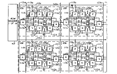
Referring now to Figures 4A and 4B, which are
: placed together as indicated to form Figure 4, random
20 ~access memory t~AM) 40 comprises an array of RAM cells
41.::It will be understood by thos~ having skill in the
art that RAM cells 4I may be SRAM cells or DRAM cells,
: and may use cell d~signs well known to those having
skill in~thè art. As illustrated in Fi~ure 4, RAM
25 ~cells~41~are;configured in an arra~ of m rows and n
columns~. For~example, in a l2~k bit RAM, 256 rows and
5:12:columns of RAM cells may ~e used. As also shown, m
word lines 42~-~2~ are coupled to a one-of-m row
~:decoder 43 for accessing one of word lines ~2~ 2m.
30!~ ~s~a1so shown in Figure 4,~ n~pairs of bit lines 44a,
: 4~a'-44~, ~4~' a~e connected to the respective n rows
of the array. ~As will be;described below, two sets of
bit ~ines are used in R~M ~0, so tha~ bit lines ~4 are
referred to as the "primary" ~it lines.
Still referring ~o Figure 4, it may be se~n
;~ ~: that p pairs of "signal" bit lines ~5~, 45a-~Sp, 45p'
~``~::~:;
!3
`` 21~ ~60
94/061~0 . PCr/~S93/08232
~ -29-
3 are provided, with every p'th pair of primary bit lines
heing conn c~ed to a respective one o~ the signal
bit lines 45. In the example shown herein, p-16, i.e.
16 pairs of signal bit lines ~5, 45' are provided, with
~ 5 every 16th column being connected to a respective one S
j of the bit lines. In other words, bit line pairs ~41
1 ~41~ ~ 4417, 4417~ 597, 4459~' ar connect~d to signal
bit lines 45~, 45all and bit lines ~416~ 432
¦~ ~432~ 4S12~ 44S121 are connected to signal bit line
lO pair 45p, ~5p'. The signal bit lines are generally
orthogonal to the primary bit lines.
The choice of the number of signal bit line
pairs depends on several factors. In particular, it
has been found ~hat the total capacitance which loads
15 the primary bit lines 44 should be equal to or greater
: than the total capaci~ance loading ~he signal bit lines
45. The total capacitance which loads the signal bit
lines 45 is primarily due to the diffusion capacitance
of;the coupling transistors which couple the primary
20 and signal bit lines, as described below. It has been
: found that this loading capacitance should be minimized
~; to achieve the maximum memory cloxk rate and minimum
; data access time and is inversely proportional to the
nu ~ er of DLI lO ~sed to configure the system.
25 Fin~lly, the relationship between m (the number of
rowsj, n (the number of co1umns), and p (the number of
DLIs) will also d pend on the overall configuration of
: th~ RAM ~0.
Continuing with the description of Figure 4,
~; : 30 a DLI lQn~... lOp is connected to a respective signal bit
' : line 45~ 5p~. First, second and third coupling
means, 4~, ~7 and 48 respectively, are used ~o
selectively couple the primary bit lines 44 to the
first reference potential 14 (VDD~, to selecti~ely
couple the signal bit lines 45 to the second rPference
potential 2B (ground), and to selectively couple the
rImary bit lines ~4 to the signal bit lines 45. In
WO94/06120 ~ 1 4 1 ~ 6 0 PCT/VS~3/08232
~30-
particular, the first coupling means comprises n pairsof P-channel transistors 49a, 49a'-49~, ~9n' for
coupling a respec~ive primary bit line 4~a, ~4~'...44~,
44~' to VDD under control of gate inputs 51 -5ln.
Second coupling means ~7 comprises p pairs of N~channel
FETs 52a, 52~-52p, 52p~, each of which couples a
respective signal bit line ~5a, 45~a_4Sp~ 45p' to
ground ~ under control of gate 53. Finally, third
coupling means ~ is seen to include P-channel
transistors 54a, 54~'-54~, 54n~ for coupling a primary
bit line 4~ 4a~-44~, 4~ to a respective signal bit
line 45~, ~5~'~45p, 45~ under control of gate 55~-55~.
An N-channel transist~r ~6a, 56a3-56~, 56~ also
couples a respective primary bit line ~a, 44a'-44~,
15 ~4~1 to ~ respective signal bit line 45a, 45ai-45p,
45pf under control of gates 57a-57~.
As will be seen from the operati~nal
description below, the first coupling means 4~ couples
; the primary bit lines to VD~ during the idle opQration
and during the read operation and decouples at least
one o~ the primary bit line pairs from VDD during a
~:~ write operation. ~he ~econd coup~ing means ~7 couples
the signal bi~t;lines to ground during the idle
operation and decouples t~e signal bit lines from
ground during a read operation and a write operation.
Th~ thir~ coupling means~48 couples the primary bit
lines to the signal bit lines during a read and write
operation and decouples the primary bit lines and
::
i~: signal bit lines from one another during an idle
; 30 opsration. In particular, P channel transistors 54
~` couple the primary bit lines to the signal bit lines
during read operation and N-channel transistors 56
couple the primary bit lines to the signal bit lines
during a write operation.
35 OE~eration of the Random Acc~ss Memo~
.
~: :
~094~06120 2 ~ - PC~/US93/08232
-31-
The detailed operation of the random access
~ - memory ~0 (Figure ~) will now be described. The idle ~.
`I state will first be described followed by the read
~ state and then the write state~
i~ 5 ~uring the idle state, a LOW logic level is
provided to gates 51 of first coupling means 46 to turn
: all of transistors ~9 on and thereby place the primary
bit lines 44 at the power suppIy level VDD~ At the same
~ time/ a HIGH logic level is provided to input 53 to
: 10 turn on second coupling means ~7, and ~hereby couple
all of the signal bit lines 45 to ground. A high logic
le~el is applied to inputs 55 and a low logic level is
applied to inputs 57 to there~y turn transistors 5~ and
5~ of and thereby decouple the primary bit lines 44
:~.15 ~rom the signal:bit lines 45. Finally, since all of
the signal bit lines ~S are a~ ground~ all of the DLIs
; 10 are in their third or idle state with all o~ the
outE~uts 27 and 27 ~ being at ground potential . No DC
:power is consumed by the~ cirs~:uit during the idle state.
: 20 During a read operation, row decoder 43
selects one of word lines 42a...42~ to access a
particular row of RAM cell 41. ~ logic LOW signal is
applied:to input 53~to turn second coupling means ~7
off to thereby decouple ~ignal bit lines 45 from
S~ ground~ Al~though not coupled ~o ground, the
capacitance of the siqnal bit lines maintains the
sign~l bit lines near ground:potential. ~ logic LOW
; : lsve} is~maintained at~ gate~ 51 to thereby continue to
couple the:prima~y bit lines to VDD. A column decoder,
:30 not shown in:Figure 4, provides a LOW logic level to a
selected ~ne of inputs of 55~-55~ depending upon the
:column to be read. This turns on the approp~iate
transistor pai~ S~, 54~ and causes current to flow
between the associated primary bit lines ~4, 44~, and
th~ signal bit lines 4~, ~5~.
It should be noted that FETs 54 are co~nected
as current controlled devices, the current through
~ WO9~/06~20 ~ 8 ~ ~ P~T/US93/08232 t
,
-32-
I which is controlled by their source voltage.
I Accordingly, the primary bit line which is at a higher
voltage will produce more current to-pull up the signal
bit lines, than the primary bit line which is at a
1 5 lower Yoltage. Since the selected RAM cell current
tries to discharge one or the other side of the primary
bit lines ~ ', the voltage of one of the primary
bit lines drops from VDD a~ a rate faster than the
other, depending on the state of the selected RAM cell
~: 10 41. Current flows ~etween the selec~ed primary bit
line pair 4~, 4~, and the si~nal bits lines 45, 45',
causing a dif~erence to occur in the voltage ramp-up
¦~ rate on the signal bit line:pair ~5, ~51, When the
ramp-up voltage on one or the other of the signal bit
: 15 lines 45, 45' exceeds the threshold of th~ ~LI ZO, the
~; output of the DLI is rapidly latched to a ONE or ZERO.
: In other words, either output 27 goes HIGH and 27' goes
LOW or output 27~ goes HI~H and 27 goes LOW.
As described in de~ail below, the outputs 27
20 of all of the DLIs may be gated ~ORed) together because
all of the DLIs which are not:active are in their third
~: ~
state. Accordingly,:the output of~the activated DLI
:~: may be placed in a read regis~er and proYided as the
chip output, as described in detail below.
Once a DLI has been latched and the data has
:: :
been read, the:RAM is rapidly restored to the idle
state by activating the MOP input 28 (Figur~ 1) with a
logic LOW signal, to immediately pull the DLI back to
: its idle state. At the same time, once the data has
been read, a HIG~ signal is applied to input 53 ~o
hereby reacti~a~e second coupling means to return th!e
signal bit lines to ground and a ~IGH signal is applied
to input 55 to decouple primary bit lines 44, 4~' f~om
signal bit lines g5, 45~. Once this has occurred, the
MOP input 28 is again brought HI~H to disable the
second pUll-up circuit ~9 because the DLI is now in the
reset state. The operation of the control circuits for
~ I
~1418~0
.W~94/~6~2~ PCT/US93/Og~32
~`'`":
-33-
restoring the RAM after a read operation will be
described in detail below.
From the above des~ription it may be seen
that the read operation is self~iming. In other
words, once the data has been read, ~he RAM resets
itself to the idle state without the need for a reset
clock pulse. Accordingly, speed is not hampered by
clocking requirements, and operations can occur 35 fast
as possible consistent with reliable reading o~ data.
The DLI also provides reliable reading of data at high
speed, so tha~ high speed operation of RAM ~0 may be
: obtained.
In the wri~e operation, a selected one of
inputs 51a-51n is placed HIG~ by a column decoder to
thereby deactivate the associated ~irst coupling means
46 and th~re~y decouple the associated pair of primary
bit lines ~ 4' from VDD. A ~ logic signal i5
applied to select one of inputs 57~-57~ to thereby
coupIe the selected primary bi~ lines 44, 44 t to the
~ 20 appropriate signàl bit lines ~5, 451. One of the
: : signal bit lines is clamped at ~OW level which thereby
:~ forces one of the selected primar~ bit lines to ground.
~: This forces one side of the selected RAM cell to ground
and cau~es the other side to go up thereby storin~ data
25 in the sel~cted cell. During the write operation,
:
transistors 54:are maintained off and ~ransistors 52
ar~ turned off to decouple the signal bit lines from
ground.~ After the write operation is successfully
performed, the written data is automatically sensed by
30 the associated DLI, and the memory is reset as
'described~above for the read operation. The operation
of the control circui~s for restoring the R~M after a
write operation will be described in detail below. a
: Having described the general operation of the
35 RAM of the Parent Applications, the detailed circuitry
for controlling th op ration of the RAM will now be
describ~d.
,
o~ oo~ o ~ u ~ f 1 ~ 1 Q ~ ~
o ~ ~ ~ ~ o ~ ~ 9 ~ (~ ~ u
~ '~ ~ o ~ t~ 2 t ~ ~ .
o~t D ~
-34 -
Read_and Write Control Circuit
Reerring now to Figure 5, there i9 illustrated
a schematic circult dia5ram ol the circuit Lor coupling
eacn o~ ~ sicnal bit line pairs 45a, ~5a~-~5p, 45~ -o a
5 DLI lOa-lOp a~d coupling the outputs 27, 27~ o~ each 3L-~
to a data out~ut register. Circuitry for refere~cirg the
signal ~it li~e pairs 45a, 45a'-45p, ~Sp' to srounc. is
also shown along with circuitry to control the binary ~
value written into a selected R~M cell 41 from a gi-~e~
1~ signal bit line pair. - -
; ~ Referring again to Figure S, each of the output .
terminals 27, ~7' of a DLI 10, for example, output ....
- term}nals 27p, 27p' ol DLI lOp, is shown coupled to a p- -- -
input Com~lementary Logic Input Parallel Cloc~ed OR gate '- -
61, 61' also referred to as a CLIP-C OR gate. The C~I -C
OR gate is described in detail in U.S. Patent No.
O ~, . .
5,2g7,212 entitled Complementary Logl~ Input ~arallel
(CLID) Logic C~ rcui t .r~mily by the present inventor
Albert W. Vinal and assisned to the assigne- oL the
~arent Ap~lications, the disclosure OL which is
lncorporated herein by reference. Conventional cascaded
OR gates may also be used; however~as described in the
aforesaid copending application, a si~gle CLIP-C OR gate
can handle large nu~bers of inputs ~t high speed and low
power.
As shown, ou~tputs 271-27~ and 27l'-27~1~ of the
; remaining DLI circuits lQl-lOpl drive other input ~terminaIs of these CLIP-C OR gates. The logic out~ut 78,
78' of each CLIP-C OR gate drives the in~ut of a transfer
, 30 memory (TR~M) output cell 62 comprisins a p~ir OL cross-
coupled complemen~ary inverters, via coupling transis~ors
63, 63'. As shown, il output 27p ol DLI lOp 's HIGr,
then N-channel transistor 63 is turned on and the lert :~
side of TR~M cell 5a is ~riven LOW. Alternatively, 1-
`~ 35 output 27p' of DLI lOp ls HIGH, then N-channel transistor
63~ is turned on via CLIP OR gate Sl' and the out~ut o~ -
TR~M cell 62 is HIGX. The cloc~
, .
~ ~ AMEN~ED SHEET
~ o ~ o ~ r ~ 2 1 4 ~ ~
O 9 0 ~
-35-
inDuts 75, 75' to CLIP-C OR gates 61, 61' will he
desc_ibed below, in connection with Figure 7. The
outputs 78, 78' o_ OR gates ~1, 61' are also provided to
reset circuit a8 oL Figure 7, via lines 77, 77~ as
5 described below. :~
As shown, the output 64 of TP~M c-ll 62 is ---
couplea to a ring segment buffer 65 having four stages,
;` to allow the output of the~T~M cell ~o ra~idly drive .~
ofI_chip or on-chip load capacitance with a specified -- -
10 voltage rise and delay time. The ring se~ment ~uffer - -
design is described in U.~S. Patent No. 5,030,853 entitled
Hlgh S~eed ~Log~c and :Memory~ ~arnily Using Ring S~ment
Buffer by the present inven:tor Albert W. Vinal assigned ,~
to the assignee of the Parent Applications, the - -
disclosure of which is hereby incorporated he~ein by
ref2re~ce. The output 66 o the ring segment buffer 65 : . :
is the digital data output oL the memory array. ~O
; AccsrainGly, durin~ a read operation, one
output o_ one DL:I will go HIC-r~ as a function o~ the
:: 20 voltage ram~ differential on the associated signal bit
. line. One input~to OR-gate 61, or one input to OR gate
:: 62 will thereby go HIG~. One of OR gate outDuts 78 or
78~ wiIl thereby go ~IGH, thereby setting or resetting
TR~M 62~. The output of T~M 62 drives ring sesment
buffer 65, to thereby provide a HIG~ or LOW data in~ut.
The ring se~ment:buffer 65 may be configured as a
trista~te driver, under~ control of a chip select signal,
~ in order to ac~om~modate a p~urality of ~ outputs on a
l~ single bus.
30 ~ S~ referring to Figure 5, when the R3~ s in
its idle s~ate, the gates or transistors 52p,. 52p' are
H-~C-'~ becaus~ the MOP gate 28 is LO~ causing the output 53
of complementary inverter 63 to be HIG~. The a~te input
t~rm~nals OL ~he transistors in inve~ter ~9 are driven by
: 39 the ~OP Sat~ 28. G-neration of the MOP signal is
cesc_ibed in detail below. In the absence of
f~
f:~
~ A~N~S~E~
f~
W~94~061~0 2 ~ ~ 1 8 ~ O PC~/US93t~8232 ~ j
36-
a MOP gate 28, each bit line of all signal bit line
pairs is continually referenced to ground by
transistors 52, 521. Voltage referencing is terminated
only when a MQP gate is active.
During a write interval, transistors ~7,
and 71 provide means for controlling the binary state
¦ written into a selected RAM cell. A RAM cell selection
occurs at the intersection of a selected word line 42
and a selected primary bit line pair ~5 (Figure 4).
The gate input tarminals of transistors 67, 67~, ar~
coupled through a lo~ic AND ga~e (not shown), to the
ONE and ZE~O output terminals respectively, of a binary
data input register described below in connection with
Figure 6.
During a write in~erval, the gate inpu~ 6~ to
transistor 71 is brought HIGH, thereby clamping the
common source connection between transistors 67 ~nd 67'
: at ground potential. Transistor 71 allows one or the
other bit line of a signal bit line pair to be clamped
to ground, depending on whether the gate voltage is
~ applied to ~ransistor 67 or 67~. If the data input
¦; register contains a binary ONE, th~n transist~rs 67 and
71 conduct, cl~mping the ZERO side 20 of ~he signal bit
line pair to ground, At the same time, the ONE side of
the signal bit line pair 20' is not clamped to ground.
The oppo~ite conditions exist if the data input
1~ -
register produces an UP level voltage at the gate of
transistor 67~ and a DOWN voltage at the gate of
transistor 67.
; 30 Figure 6 illus~ra~es the data input r gister
70. As shown, a data input 76 to the RAM array is
coupled to a transfer memory output cell 73, the ZERO
output of which is coupled to a first ring segment
buf~er 74 and the ONE output of which is coupled to a
;~;35 second ring se~ment ~uffer 74' to produce a 2ERO output
:~7~' or a ONE output 7~ which is coupled to the input
72, 72' of Figure 5. The ring segment buffer is
;:
0 . . ~ i . 2 ~ o
ii " . . ~ ~ 3 ~ t
t '. 9 ~
_37_ !
descriDea in the aforesala u.S. Patent 5, 030, 853 . IL
allows a given load to be driven, with a prece~erminec
ris2 time, and minimum delay.
The data inout register circuit 70 allows a
S slow rise time inDut to be converted into raSt rise time
TRUE and COMPLEM_NT outputs, with a minimum ~elay.
Accordinqly, the circuit o~ Figure 5 may also be used to
buf~er slow ris2 time ~M in~uts (such as addr-ss or .--- o
select inputsj, for use in the RAM array. .-~
Continuing with the description or the write
operation, and referring again to Figure 4, assume that a
particular primary ~lt l_ne~pair 44, 44' iâ decoded and
activated by bit line decoder. Transistors 49, 49' o~
this bit line pair are turned off during a wrl~e cycle by c- O
selecting the ap~ropriate input 51 via the bit line
decoder. ADproQriate decoded coupling transis.ors 56,
56' are tur~ed on. One side or the other or a sisnal bit
.~
"~ line oair 45, 45' is clamped to ground by the datG inou~ -
;~ r-gister via trznsistors 67:! 67' (Figure 5~. This causes
; 20 the associa~ed transisto~r 56, 56' (Figure a) to pull aown
; one primary bit line ~4, 44i.towards ground potential.
The unclamped signal bit line rapid~y rises in voltage
unti~ the sum of~this voltage and the drop in the primary
bit llne voltage equals the power supply voltage ~D.
Preferably, the R~M cell design allows the inc~_ase in
~; the~unclampe~ signal bit~line voltage to be e~ual ~o the
decrease in the primary signal bit line voltage.
; During a write cycle, one or m word lines a2 is
also turned on by row decoder 43 (Fi~u~- a ), aoolyins
(galt~voltage~to~!the pass transistors o~ the R~ c-ll.~
The selected R~M cell pass transistors ther-~y couole -he
; ;potential o~ the primary bit lines to or from a common
signal point in the R~M cell. During write, the primary
bit line ehat is~driven to near ground potential s~ts ~e
state of the selected R~ cell. When the stat~ o_ the
selected R~ cell is
~: ~
'~
AMNI l~n ~FET
WO~4/0612~ 2 1 ~ O PCT/US93J08232
-38-
set, the MOP ga~e generator described below is
terminated along with the write gate 68 (Figure 53, and
transistors ~9, 49~ are turned on t~ recharge the 1-
primary bit lines ~4 back to power supply voltage VDD. I
Simultan~ously, transistor 71 of Figure 5 is turned off
and transistors 52, 52~ are turned on allowing both
signal bi.t lines 45, 45~ to be returned to ground '.
potential.
During the write interval, the rising
potential of the unclamped signal bit line rapidly
. causes the associated DLI to respond to this signal
: voltage when it exceeds the threshold voltage of the
DLI. The binary state written into the RAM cell is
therefore also transmitted to the output TRAM 62
(Figure 5) and presented to the output 6~, as described
above for the read operation, allowing error detection
functions to be performed~ It will be understood by
~: those having skill in the art that the simultaneous
~ sensing of the signal voltage writ~en into ~he selected
: 20 RA~ cell during a write operation allows the RAM to
terminate the write operation without the need for
external clocking~ Resetting of tpe RAM after a write
or read operation will be described below.
emor~ QPeration (MOP) Timinq Gontro!
~: 25 Referriny now to Figure 7, the circuitry for
controlling the timing of a read and write operation,
collectively referred to as a memory operation ~MOP) is
shown. ~his circuitry generates a MOP signal which is
used at ~arious portions of the RAM architecture as
30 `~reviously described. Activ~ion of the MOP signal
initiates a read or write operation, and deactivation
of the MOP signal terminates the r~ad or write .
operation, as described below. By yenerating an
internal M9P signal, and using the MOP signal to
control the timing of read and write operations, the
memory operation is independent of an external clock.
:'
:::
~WO94/06120 ~ , , PCT/US93/08232
., . . . I
-39-
System power is dissipated only during the MOP
interval, and is primarily related to the switching
power; i.e. it is proportional to capacitance times
voltage squared times the switching frequency. When
the MOP gate is of~, the only power dissipated by the
sy~tem is due to transistor leakage current. None of
the circuits within the system dissipate standby power
~: when the memory is not functioning in a read or write
: mode, regardless of whether the chip select is active
or not. A low power, high speed memory is thereby
~ : provided. :~
:~ Moreover, sinc~ the memory creates its own
timing signals for read and write operations, all
~ iming and logic functions within the memory are
; l5 automatically temperature compensated, a~lowing ~he RAM
to reliably operate over a broad range of temperatures.
: At high temperatures, the maximum access rate is
:: lowered from room temperature due to the reduced
current ~apabiIities~ of the transistors. A~ low
0 temperatures:, the maximum access:rate is increased
: above the room temperature value due to the increased
current capabilities of the transi~tor.
eferring again to Figure 7, the read/write
operation:timing circui~ry~0 is controlled by a TRAM
25 cell:~82 comprising a pair of cross-coupled inverters
and~a pair;of pass transistors:of well known design.
This~:TRAM cell is turned on and the output 83 thereof
goes HTGH when a:n address change detection system
; issues an address changP detection clDck pulse on input
30 85, upon detecting a change in the input address. This
TRAM cel~l i5` also turned on when a chip sel~ect
transition going active, or a~write enablP tr~nsition
: going active, is detected by a TDLU discussed below in ~
connection with Figure 8~ The address change detection t
35 ystem is described in connection with Figure 8 below.
The output 83 of RAM cell 82 is~coupled to a
ring seg~ent buffer 86, the output of which is coupled
,
t
W~4/06120 ~ llll 3 6 0 PCT/US93108232
-40-
to a group of ring segment buffers a4~ These ring
segment buffers provide the mechanism for driving the
total load capacity associat~d wi~h the clock lines and
the system logic cells such as the bit and word address
decoding drivers and the DLI sensing systems. These
ring segment buffers also provide the proper delay for
timing the various internal circuits in the RAM, as
described ~elow.
As shown in Figure 7, five delay ring segment
buffers 84a-84e are used, however other numbers of ring
s~gment buffers may be used in other memory
architectures. Ring segment buffers 8~a and 84b are
used to clock the bit decoders ~-not shown) for the
primary bit line pairs, and ring seyment buffers ~c
and 84~ are used to clock the row decoder 43 (~igure
1 4). The input stage of each of ring segment buffers
¦ ~ 8~ a comprise a two input CMOS NAND gate. One of
: the input gate electrodes of this N~ND gate is driven
~:~ by the appropriate output of the high order bit of the
1~ 20 m bit word a~d n bit address registers. The other
input is drive~ by the MOP gate. This NAND gate
¦ ~ permits segmenting the total numbe~ of row and column
selects of the RAM into at least two halves. The first
half contains m/2 low order addresses and n/2 high
~rder addresses. Accordingly, clocking in high order
groups is inhibited when addressing low order group
~; ~ selection and vice versa. This procedure eliminates
: di sipatin~ unnecessary wi~ching power during a read
.
~; or write memory cycle and simplifies the design of the
clock driver. However, it will be understood by tho~e
~ hàving skill in the art that the word and ~it decode ~}
¦~ functions need not be divided into groups.
~:; The output of d lay ring segment buffer 84e
~:~ is provided to the DLI input 2~ (Figures l and 5) and
i . 35 to the clock inputs of the CLIP-C OR circuits 75, 7~'
¦; ~Figure 5~. Accordingly, after a predetermined period
~ from the time an address change is detected, the DLI
2141~0
~W~94/06120 PCT/US93/~Z32.
-41-
input ~8 is activated and a clock pulse is applied to
the CLIP-C OR gate. Application of the MOP input 28 to
- the DLI lO of Figure 1, allows the DLI to rapidly latch S
into one or the other ~inary state, without
5 interference from the second pull-up circuit 29, 29'.
Application of the MOP input to clocking inputs of the
CLIP-C OR gates 75 provides a clock pulse for timing
the output of the CLIP-C OR gate.
Still referring to Figure 7, two input CMOS
OR gate 88 is drlven ~y the outputs 77, 77~ of the p-
input CLIP-C OR gates 61, 61~ (Figure 5). The reset
output 81 of this OR gate resets TRAM 82 and thereby
resets each ring segment buffer 84 after the
: predetermined delay of each ring segment buffer. After
a RAM cell has been read (either during a read cycl~ or
at the end of a write cycle~ one or the other p-input
CLIP-C OR gates 61, 61~ (Figure 6) will deliver a logic
HIGH voltage at outpu~ 71 or 71~, to signal completion
of the intended operation. In other words, a DLI has
properly stored a bit value which was read or has
properly stored a bit ~alue which was written to
~: confirm that writing has taken pl~ce. When this event
occurs, the MOP gate is no longer required and is
automatically terminated by action of the MOP ga~e
reset dri~er 88. All clock drivers subsequently shut
down within~the propagation delay time of the ring
agment buffers 84.
In particular, ring segment buffers ~4a and
: 84~shut down the bit decoders an~ ring segment buffers
30 ~40 and 8~ shu~ down the word decoders 43 ~Figure 4).
:
Ring seg~ent buffPr 84c terminates the MOP signal which~
shuts of~ CLIP-C OR gates 61, 6~ (Figure 5) and also
causes second pull-up circuits 29, 29~ ~Figure 1) to
rapidly bring D~I 10 to its reset stat (both inputs at
: 35 ground). A memory operation (read or write) is thereby .
automatically terminated.
1~' ~ ..... .
WO9~/06120 2 ~ ~13 6 ~ PCT/US93/08232
-42-
From the above description it may be seen
that th feedbacX shutdown control of the NOP gate
generator automatically accommodates broad thermal
environments that ~he RAM may experience, since MOP
shutdown occurs only after a read or write function
completion has been detected by the DLI. In other
words, the MOP gate is initiated when either an address
change, chip select or write enable is detected,
indicating that a r~ad or write operation is to begin,
and is automatically terminated once the proper read or
writ~ function has been completed. When neither a
write or read function is required, the M~P gate is off
: and remains off un~il tur~ed on again by the output of
the change detector. The address change detector
operation will be described in the next section in
: connection with Figure 8.
Address Chan~ Detection System
In general, a random access memory can begin
a memory operation ~i.e. a read or a write operation~
by detecting a change in at least one of thP input
address bits. In a conventional ~ddress change
~ detection system, the time required to detect a change
¦ in the input address can significantly slow the memory
cycle time. According to ~he Parent Applications, an
~: 25 improved addxess change detection system detects a
change in an input:address in minimum time. The system
; : uses a ~ransition detection logic unit ~TDLU) which is
hown in ~igure 8. :Pri~r to descri~ing the TDLU, a
:~ conventional address change detection system will be
~ 30`idescrib~d.
I : There are three basic elements r~quired in a
conventional address change dete~tion system. The
first is a latch which i used to increase the rise
ime of the input address bit. Using the examplP of a
memory with m rows and n columns, a total of m+n
latches are required to compare the m+n latches allow
2 1 ~
~ ~94/06120 - PCT/US93/0823~ -
.,.. . , .
-43-
comparison of the m~n address bits. The second
component of a conventional address change detection ~.
I system is an excluci~e OR circuit for each of the
¦ latches. The exclusive OR circuit will provide an
S output whenever the previous address bit and the
present address bit are different. Finally, all of the
~:- exclusive OR gate outputs are ORed together, to provide
HIGH logic level when any of the exclusive OR ~ates
are HIGH~ A change in the address is thereby detected.
The above described exclusive OR and OR logic
: is responsible for mos~ of:the delay in detecting the
change in th~ input address, due to the large number of
inputs which~have to be ORed together. For example,
for a 64k bit RAM, the total nu~ber of address bits
(m+n) is 16, and for;a 256k bit RAM the total number of
address bits (m+n) is e~ual to 18. Using conventional
~; CMOS:g~tes,:a cascaded:tree:of CMOS gates is required
~ : :
:~ to provide the function of a 16 or 18 input OR gate.
For example, using conventional three input
~CMOS OR gates,:a nine-OR gate tree is necessary to OR
18 inputs. six~o~ gates accept the total of 18 inputs
at a first level of the tree. The ~utputs of each
~,;~; . ~ , .
group of:three gates are provided to an OR gate at a
: second level. Two OR gates are used in the econd
::: 25 level to~accept all six ou~puts from the first levelO
: Finally, at a ~hird level, one OR gate combines the
o~tput~of the two second level OR gates. Propagation
delay time:through this~logic tree is excessive and
.~ requires many ~ransistors~to perform the ~unction.
: 30 ~eferring~now to Figure 8, a block diagram of
:the~address~change detection system! 9o of the Parent
: : Appl~ications will now be de~cri~ed. As shown, the
address change detection:system comprises m~n
Transition Detection Delay Units (TDLU) 9~a-9~
respective~address:bit 91a-91D is provided ~s the input
; to a r spective~transition detection delay unit 92a-
92n. The respective outputs 93~-93n of the transition :
,~
O ~ ~ - a ~ q ~
,~ ~ D ~ S ~
~ 9, 0 ~ % ~ ~
-~a_
detection delay units 92a-~2n are provided as inDuts ~ a
single m+n inpu~ Com~lementary Logic InDut Para
(CI.I~) OR gate 102. The outDut 85 of C~IP OR sate 102
provides an address change detection sisnal which is J
5 provided to the I~OP generatin5 circuit 80 or Figure 7. 1,
The desicn a~d oDeratlon of a complementa~y logic i--~ut ~ ~o
parallel OR circuit 102 is described in the
aforementioned U.S. Patent No. 5,2g7,212. .... :.
~ach TDLU 92 delivers a cloc.~ PU1S2 to the .~
appropriate input or the CLIP OR ~ate 102 when an adaress - -
transition is detected on its lnput add~ess line 91. One
: T~LU is cou~led to the chip select latch and one TDLU is : :
coupled to the write enable latch (not shown). Their
outputs are also inputted tO CLIP OR gate 102. The basic .
15 components OL the TDLU are a latch 94a-94n, whose logical
: stat~ is controlled ~y a single input signal,line 91~-91~ q
~: which is connected to the address inputs or the R~-M chi?. .. .
The ON and ZERO outputs or the latch, 95a-95n and 95a~
: 95n' respectlvely,: rapidly switch when a transition in
:
the inPut signal 91 occurs ~nd provides both the TRU~ and
COMP~EMENT Iunction of the input sig~al. Identical ring
.~
:~ ~ segment buffers 96a-96n and:96a'-96~' are coupled to the
;~ true and complement outputs:95a-95n and 95a'-9Sn' of ~he
latches 94a-94n, As shown in Figure 8, ring segment
2:5 ~ buffers 96 are delay ring segment buffers with an odd
number of st~ges to provide an inverting delay ring
sesment buffer (RSB-I).: The design and operation or a
delay rlng~segment bu~fer is described in U.S. Patent ~o. t
5,030,~53. As~described in this application, the aelaY
prd~er~y of the~ring segment buffer is controlled by
proper choice of channel length for the P- and N-chan~el
: : transistors used to form the ring segment bu~Ler
inverters:. The outputs of the ring segment burrers and
the outDuts of the latch are each connected to cascaed
N~D sates
AME~ F~sHEET
~ : . .
2 1 ~ i3 ....
094/Q6120 PCT/US93/08232 -
-45-
98~-9~n as illustrated in Figure 8, to form the output
93~93~ of the TDLUs ~2~-92~. 1
Figure 9 illustrates an alternative design
for the TDLU ~2. In this alternative design,
noninverting delay ring segment buf~ers, consisting of
an even number of inverter stages, are used. The latch
outputs 95~ ~5' are cross-coupled with the ring se~ment
buffer outputs in order to provide the proper inputs to
the cascaded NAND gates ~8. Figure 10 illustrates the
relationship between the input address bit 91 and the
output 93 of each of the TDLUs g2, 92' o~ Figures ~ or
9. As shown; a positive going or negative going
transition in an address bit 3I provides a clock pulse
of a~predetermined duration at the sutput 93. The
duration of the clock pulse resulting from detecting a
transition at the outputs of the latrh, is controlled
: by the time delay designed into the ring segment
buffers 96.- ~ ~
Figures llA and llB illustrate ~he truth
tables for the TDLU 92 of Figure ~ and the TDLU 92 ! of
: Figure g, respe~ctively. Referring to Figures llA and
, it may be seen khat both conf~gurations of the
TDLU produce the same output function for the same
input function.
; The address change detec~ion system of the
Parent Applica~ions, is simple to construct and
: ~irtually eliminates propagation delay time required to
detect a change in an input ~oltage function, and has
broad functional:application for high speed computer
30 design philosophy. It will also be noted that the TDLU :~
~ .
echnology automatically accommodates the demands ofl ` }
the MOP gate generator for temperature effects.
Figures 12A:a~d 12~, which together form
Figure I2 as indicated, illustrat~ a circuit schematic
35 diagram of the ad~ress change de~ection circuitry of
Figure 8. As shown, TRAM 92 includes latch 94 and a
; pair of three stage (inverting) ring segment buffers
W094JO~1~0 2l ql 8 ~ .. PCT/VS93/~8232 ~,
: -46
~6, ~6~. Complementary Logic Input Parallel NAND ga~es
99, 100 and 101 are also shown. ~ssuminq equal channel
lengths, the relative channel widths of the respective
transistors are shown within the respective
transistors.
The outpu~ 93 from the transi~ion detection
delay unit 92 is provided as an input to multiple input
CLIP OR gate 102. The corresponding outpu~s fro~ the
other transition detection delay units are also
prcvided as inputs to the CLIP OR gate ~02r Also
provided as an input to ~he CLIP OR gate is a chip
I
salect input 103 so that the output ~5 of CLIP OR gate
10~ is at logic ~IGH whenever an address change is
~ detected and the ~AM chip has been selected.
Timin~ of RAM Operation
Having now described the individual
components an~ the detailed operation of the Parent
Appli ations, an: Gvervi2w of the memory timing will now
be described in connection with the timing diagram of
Figure 13. The time line of Figure 13 is calibrated in
nanoseconds and~the values ar~ bas~d on simulations of
. the RA~ of the Parent Applications, with the FETs being
fabricated using 0.8 micron groundrules.
The timing diagram be~ins at time equals
Zero, with a:change on input address ~1 o~ ~igure 8.
The change in input-address is detected and the output
: 85~of the addr~ss change detection system o~ Figure 8
is produc~d after 1.~ nanosecsnds. This output is
provided to the:timing circuit ~0 of Figure 7, and the
30' output of ring segmen~ buffer 84e produces the MOP
signal ~fter about 1.75 na~oseconds. At abou~ 3.5
nanoseconds, the bit decoders and word decoders are
clocked via the outputs o~ ring segment buffers 84a-~4d
of Figur 7. Accordingly, ~he read or write interval
begins after about 305 nanoseconds from the tim~ the
input address changed~
~iW~94J~612~ 2 ~ ` PCT/~S93/~8~32
.
-47-
~n output is produced on the DLI at just over
flYe nanoseconds and the MOP reset signal ~1 of Figure
7 is produced shortly therea~ter. The data out signal
66 in Figure 5 is produced approximately 2.7
` 5 nanoseconds from the time the read/write interval
began. The reset signal propaga~es through the ring
segment buffers 84~-84e between five and six
nanoseconds to turn off the CLIP-C O~ gate 7~, 75' of
Figure 5 and to activate the second pull-up circuit of
the DLI via ~P input 28. ~ccordingly, a~ter about
seYen nanoseconds, a new read/wrlte cycle may start
with a new change in the input ~ddress.
; The random access memory of the Parent
Applications may also be operated in a unique write
mode called "burst write". Burst write is achieved
when the~write:enable is active, the chip select (103,
Figure 12):is active, an~ the ~ransition detection
delay unit output starts the memory cycle with each
detected address change and the DLI output ~erminates
~the MOP gate. This burst write cycle can be used
efficiently to fully load all or a part of the total
memory in minimal time and with m~nimal power
consumption. :~ : :
~: :
;~ mproved Goupling Be~een Prima~ and Si~nal Bit Lines
25;; ~The memo~y~architecture of FigurPs 4~ and 4B
inc;ludes~a~first coupling means ~9 for coupling a
: : primary~bit line ~4 to VDD under control;of gate inputs
51. ~A third coupling means 48 couples at least one
primary bit llne pair 44 Xo a respective~signal bit
` ` : 30 line pair:45. The:first and ~hird coupling means are
located;a t Dpposite ends of the primary bit lines ~4.
In particular, each of the primary bit lines includes
one ~nd~whtch is relatiYQly close to the signal bit
linas and an~opposite end which is relatively distant
3:~ from the signal bit lines. The ~irst coupling means
are located at the oppo~ite (relatively distant) end of
~. ~
. W094/06l~0 21~1S~O PCT/US93/08~32 ~ ~
48-
the primary bit lines and the third coupling means are
~; located at the one (relatively close) end of the
primary bit lines, adjacent the signal bit lines.
~ In the configuration of Figures 4A and 4B it
;~ 5 has bfen found that the remote positioning of the first
coupling means may degrade the performance of the RAM.
In particular, the performance of ths third coupling
~ means may be degraded by the electrical resistance of
i~ the primary bi~ lines ~4. When the first coupling
means ~g i5 loca~ed at the opposite end of the primary
~ bit lines, t~e pull-up transistors remain on and serve
'j to control the source voltage of the pass transistors
: 5~ in the third coupling m ans. These pass transistors
~ shuttle current from the primary bit lines to one of
.~ 15 the signal bit line pairs ~5. ~he amount of shu~tle
current decreases with increasing source voltage.. The
~:~ differance in source voltage o~ the P-channel
~ ~ .
transistors 54 in the third coupling means accounts for
the dif~'erential component of the current which is
shuttled through the signal bit lines. This
differential current component is produced by current
~ flowing to ground from one side or~the other of the
; ` primary bit lines as a resl~lt of a selected ~AM cell
; ~ during a data read operation. The difference in the
25 shuttle current: accounts for the difference in the
:: : ~ :
voltage ramp~up rate o~ the selected bit line detected
: by the DLI 10.
:: The remote position of the first coupling
ans 4~ of Figure ~ allows the shut~le current to flow
30 through the primary bit lines 44. Unfortlmately, this
urrent produces an additional voltage drop at the
source terminal of the ~ransistors 5~ in thf third
coupling means,~ due ~o the resistance of the primary ~ ¦
bit lines 4~ This additional vol~age drop reduces
35 shuttle current and thereby increases the ramp-up time ' t
t
~ on the signal bit lines, thereby delaying detection of
3~ the state of th~ selected RAM cell.
~,WO94/06120 2 1 ~ 1 5 ~ ~ PCT/US93/08232
;~'"' ' i
-49-
Moreover, a significant imbalance may occur
in the resistance of one of the main bit lines of each
main bit line pair as a result of manu~acturing
imperfections. This resistance imbalance may increase
the probability of a fa~se signal being detected by the
~LI. Finally, the remote position of the ~irst
coupling means 49 requires a conductor to run along the
length of each primary bit line pair 44 in order to
` terminate the pull-up current on a selected bit line
pair during a write operation. In other words,
terminals:51 and 57 are~connected by running a
` conductor line across the entire length of the main bit
: line. These conductor lines add to the complexity of
: the RAM layout. `
~, ~ ; 15 Figures 14A and 14B, which when placed
~: together form Figure 14, describe a solution to all of
:
these probiems.::As shown in Figures 14A and 14B, thP
firs~ coupling:means 49 is~pos:itioned at the one end 6fi
:; of~the primary bit lines ~4, relatively cl~se to the
20: signal bi~ lines 45~, rather than being positioned at
the opposite e~d 65 of the primary bit lines 4~,
relatively distant from the~signal bit lines 45. By
positioning the~first coupling means at tha one end of
; thè~primary bit~lines, close to the~third coupling
2~5~ means,~it~1ine resistance:~effects are eliminated.
Accordingly,~the re~uced shuttle current due to prlmary
bit l~ine:voltage~drop is~eliminated, and~sensing deIay~
is ~educed. Moreover, an imbalance in the resistance
of;one~or~the~other primary bit l;ines as~a~result of
manufacturing~imperfecti~ns does not ad~ersely impact
the~accurate sens~ing of;da~a read from a ~selected RAM
cell. Finally, the placement of the firs~ coupling
m~an~s adjacent the third~c~oupling means allows
terminals 51~ and 57:~o be electrically:connected using
a~short~conductor line,~which nead not run the entire
length of~tne primary~:bit lines.
, ' . ! : ` ' .
W~9~/06120 PCT/US93/08232 ~;
214l~60
-50
It will be understood by those having skill
in the art that in the conf1guration shown in Figure
14, the main bit lines ~4 become stub transmission
lines with no termination at the opposite end 65. RAM
cells which are located toward the opposite end 65 are
therefore not sensed immediately at the one end ~6 due
to transmission line delay ~ime. The maximum delay
: time Td is ~iven by the following equation:
: :
Td 2 [ I~ Rl]
: :
~here î
V0 ~ is the valtage operating point of the
first coupling ~ransistor 49~with full shu~tle current
flowing, typical 0.5 Volts.
:
DD = Power supply voltage.
Cl = Total capacitance of the main bit line
,~,,40 ~ ~
IM~ - RAM cell 41 curren~.
Rl =:Electrical resistance of the main bit
:: :
line 44. ~ ~ -
For a~RAM~architecture which:includes 256 RAM cells 47
per~main bit line pair ~4, the delay time Td iS
typically 200:picoseconds. :This delay may b2
: accommodated ~y activating a selected word line 42
~prior to~activating the selected transistor 5~ in the
~' third coupling means by a time equal to the worst main
~ as ~ bit line delay time Td.
A number o~ alternate embodiments for the
first and third coupling means are illustrated in
Figures ~-l9.~ It will be understood by those h ving
skill ln th art that:the first coupling means may be
: 30 located at the opposite (far3 end 65 of the primary bit
~:
2 ~
~94/0612~ P~T/US93/~232
-51-
lines 44, as was illustra~ed in Figure 4. Preferably,
however, the first coupling means is located at the one
~ (near) end 66 of the primary bit lines as illustrated
d~ in Figures 14A and 14B. Other embodiments o~ the first
and third coupling means will also be envisioned by
those having skill in the art.
In ord r to simplify Fi~ures 15-l9, only a
single first coup1ing means ~6 and a single third
coupling means 48 are shown. However, it will be
: lO understood by those having skill in the ar~ that a
plura1ity of f1rst coupling means ~6 and third coupling
means 4~ may be substituted into Figures 14A and 14B.
Xe~erring now to~Figure 15, the embodimant
shown includes third coupling means 4~ which is
;~` 15 identical to that shown in Figure 14. However, first
~ coupling means 46 adds a pair of cross coupled P type
`;~ ransistors:6l,~6l~, ~he control1ed electrodes of which
`~ are~serially~coupled b tween;power supply ~oltage VDD
and:a r~spective one of ~he primary bit lines 44, 44'.
The~controlling:;eIectrodes are cross coupled to a
: respective:one of the associated signal bit lines 45',
`~ 45~ ~he ch nnel widths and length~ of all of the P
channe1~transistors ~1, 61~,:and ~9, 49~ are identical.
~ Tha tran istors:.61, 61~ provide an analog
`~ 25 feedback~path:~from the~signal:b~it lines to the first
coupling means to enh~nce ~he RAM cell induced
dif~erential~:signal:component which is shuttled from
the~;~:ma~i;n bit~lines~ ~to the signal bit lines.: The effect
: o~ thiæ feedback confIgurat:ion i~ to almos~ double the
:~ 30 differentia1 of ~he signal~ componen~ due to R~M cell
urrent.~ The~feedback a1lows almost all of the RAM
current to~be~shuttled to the signal bi~ line as a
differential signal~, instead o~ slightly over half the
R~M~current~which is shu~tled without the use of
feedback~ Accor~ingly, the signal being detected by
the~ DL~ 20~is increased,~and smaller RAM c ll designs
ith~reduced current outputs, may ~e used.
W094tO61~0 2 ~ ~ 1 8 ~ ~ PCT/~S93/08232 ~. ,
,
52-
This feedback technique also plays a
fundamental role in controlling the voltage of each
primary bit line of the selected pair during the
writing of data. Specifically, feedback voltage
signals are cross coupled from the signal bit line to
the gates of the first coupling means, allowing one of
the selected primary bit lines to be held close to
supply voltage VDD~ while the other selec~ed memory bit
line is forced close to ~round. This technique of
utilizing feedback~control ~rom the signal bit line to
the ~irst coupling means:greatly impro~es the
reliability of writing data into a selected RAM c~ll.
: It will be understood that an additional
~ small capacitive loading of the signal bit line is
produced due to the gate capacity of ~ransistors 6~. .
However, when the Fermi threshold field effect
: transistor, described in U.S. Patent Nos. 4,990,974 and
~: ~ 4,9~4,043 (assigned to the assignee of the Parent
.
Applications) are used, this capacitive loading becomes
almost nesligible. :The embodiment of Figure 15 is
presently considered by the inventor to be the best
mode for configuring the first and third coupling means
at the first end of the primary bit lines.
: Re~erring now to Figure 16, another
aIternativ~ embodiment of the first and third coupling
: m~ans is~shown. The third coupling means ~8 i~
: identical to Figure 15. However, the first coupling
:: means~6 uses only the cross coupled pair of
transistors 61, 61' and eliminates the need for the
:; 30 transistors ~g, 49~ of Figure 15. This embodiment may
provide mor~e feedback than is necessary in some RAM
architectures.~
Referrin~ now to~th~ embodiment of Figure 17,
the third coupling means 48 is identical to Figure 16.
The first coupling means 4~ ic identical to Figure 16,
xcept that another P channel transistor 62 is added in
:::: : :
' ~ '`.
~094/06120 21~ PCT/U593/OB232
-53-
order to allow ~he transis~ors 61, 61' ~o be turned off
: during a write operation.
Figure 18 describes another embodiment of the
Parent Applications. The first coupling means 46 is
identical to Figure 14. However, the second coupling
means 4~ adds a pair of cross coupled transistors 63,
63~ to provide additional feedback and thereby amplify
the differential signal. As shown in Figure 18, the
;~ ~ additional transistors may be located between
transistors 54, 54~ and the signal bit lines 45, 45l,
Alternatively, as shown in Figure 1~, the cross coupled
: transistors ~3, 63' may be located between the first
coupling means 46 and the transistors 54, 54^.
Other embodiments of the first and third
coupling means will be envisioned by those having skill
;~ in the art, in which the first and third coupling means
are located at one end of the~primary bit lines,
adjacent the signal bit lines. The first coupling
:~
means is not located at the opposit (remote) end o~
the primary bit lines. Although it would appear to be
undesirable to allow the remote end of the primary bit
lins to act as an unterminated transmission line, it
has been unexpectedly found, both experimentally and
theore~ically,: that improved performance may be
obtained when the first coupling means are moved to the
.~ close end~of the:primary bit lines, adjacent the signal
:: bit:lines and the third coupling means.
From the above Description of a Preferred
Embodiment, it will be understood by those having skill
~ :
in the art that the Differential Latching Inverter,
emory a~chitecture, read and wri~e control cir~uit,
~ :; memory o peration timing control cirt::uit and addres~
;~ change ~detecti~n circ:ui~ may be used independently to
imp~ove the operation of conventional random ac:cess
35 memories. However, ~ it will also be understood by those
having skill in the ar~ ~ha~ these elements may all be
inco~po~ated together into a uni:que random acce~s
WO94/06120 21 1 i' g ~ PCT/U593/08232
-54-
memory design which exhibits high speed an~ low power
dissipation. Fox example, a computer simulation of a
128 kilob}t SRA~ array using thase circuits and
implemented in 0~8 micron MOSFET technology exhibits a
read or writ2 cycle time of eight nanoseconds, and a
power dissipation of 200 milliwatts operating at 125
mHz, at room temperature. The memoxy dissipates ~00
microwatts when idle. This performance is unheard of
in the present state of ~he art of S~AM design. When
0.8 micron Fermi-FET technology is employed, 200 mHz
performance i5 readily achieved with less power.
Coincident Activation of Pass Transistors
In order to describe the problems of
conventional six transistor SRAM cells, the operation
of a conventional SRAM cell in the architecture of the
Parent Applications will be described.
Figures 20A and 20~, which when placed
together f~rm Figure 20, illustra~e an array of SRAM
cells 41 opera~ing in the SRAM architecture of Figures
4A-4B and 14A-14B. It will be und~rstood by thos~
having skill~in the art that the S ~ cells 4~ may also
operate in a conventional S ~ architecture.
: As illustrated in Figure 20, an array 35 of m
rows and n columns of SRAM cells 41 is shown. Each
SR~M cell 4~ includes a pair of cross coupled
complementary inverters. The first complementary
:inverter 11~ includes an input l~lb and an outpu~ l~la,
and is comp~ised of P-channel transistor ~l~c and N-
::: :
: channel transistor llld which are serially connected
30` ~etween fi;rst and second re~erence voltag ~l typicallytha power supply voltage VD~ and ground. Inv~rter input
: lllb is the controlling electrodes ~gates) of
transistors lllc and 11 ~ and output llla is the
connection node between serially connected transistors
111G and llld. Complementary topologies can also be
used. The second complementary inverter 112 includes
WO94/06120 21~ PCI/US93/~8~2
--55
an output ~12a and an input 1~2b and is comprised of
: serially connected P-channel transistor 112c and N-
channel transistor ~12d. Inverter input 112b is the
controlling electrodes (gates) of transistors ~12c and
112~ and output 112~ is the connection node between
serially connected transistors 112c and 112~. The
~: output lll~ of the first complementary inverter 111 is
~ electricaIly connacted to the input 112b of the second
:~ ~ complementary inverter ~1~, and the output 112a of the
: 10 second inverter 112 is connected to the input ~llb of
the first inverter:lll to form a latch of cross-coupl~d
: : complementary tra~nsistor in~erters, which is capable of
storing a binary l or 0 therein~
. Also:included in~the SRAM cell ~1 is a pair
:
~: : ,15~ of pass transistors 113a and 113b. The controlled
electrodes, (source~and drain)~of the first pass
transi:sto-r ~13~ are connected between a first
associated~blt line ~4~.O.44~ and the output llla of
: :the:first complementary inverter ll~. The controlling
20~electrode (gate~) of first pass transistor 113a is
c~nnected~:to~the;associated word line 42a-42m.
.`,;~ Similarly, the:controlled~electrod~s of the second pass
: ;transistor~113~:are connected between the output 112a
of~the:~second complementary inverter 112 and an
25~ ssoclated~bit:1ine 4,4a'-~4n', and~the controlling
: :eleotrode~of t~e second pass transistor 113b is
conne~ted~to~the-~associated word llne 42a-42~. ~It will
be:understood~by~those~ha~ing skill in the art that an
'array~off~ only~ wo rows and four columns of cell~ are
:. 30~ shown in~ Figure:20. :However, typically, up to 256 or
~ore~rows fand up to 256 or more columns of cPlls may be
used:. :
:In operation,~ each~bit line 44a-4~ and ~
4~D' is referenced to positive potential such as VDD.
~In~order~to read:~or:write into a selfected cell 41, the
row decoder 43~selects the row ~2a~ f~2~ associated with
the desired cell ~ for~example by bringing the
W~94/06120 2 1 4 ~ P~T/US93/08232
~-56-
,, I
.. selected row to VDD. When the decoded word line is
energized, one o~ the pass transistors 113a or 113b in
. each of the SRAM cells ~1 connected to that row wiil
sink current to ground from ~he appropriate bit line
5 44a-4~ or ~4a~ , depending on the digital s~ate of
the R~M cell. Ac~ordinyly, i~ there are 256 RAM cells
41 in aach row, and the sink current is lmA, then 256~A
flows between yround and VDD when a word line is
3 selected. ~t the end of the word pulse upon
10 de~election of the word line, all 256 bit line pairs
are recharged back up to VnD, again resulting in
: substantial ~:ransient power co~sumption.
:
~ XeXerring now to Figures 2lA and 2lB, which
:~ when placed together as indicated form Figure 21, a
lS random access memory having coincident pass transistor
activation means accordin~ to the present invention
will now be described. It will be understood that the
i
;~ SRAM ~ell described in Figure 21 may be used in a
conventional SRAM architec~ure as well as the unique
20 architec~ure described in the Parent Applications. As
shown in Figure 21, SRAM cell llO includes a column
select line 115a ~S~ f~r each colu~n of the array.
Each column select line lI~a-~15~ is coupled to a
gating means ~6 such that the pass transistors 113 in
25 the memory cell 110 are only activated upon coincident
(simultaneous) selection of the word line 44 and column
select lin~ llS associated with that cell. Selection
of only the word line or only ~he column select line
will not activate the pa~s transistors. ~ccordingly,
30 wh~n a word line 42 is selected, all of the pa s
~ t~ansistors in the selected row will not ~e activated.
:~: Power consumption is thereby dramatically reduced. For
example, if 256 cells are included in each row,
transient power consumption is reduced to 1~256 of its
value without the coincident pass transistor activ~tion
~ means~
::~
,`.
094/06120 ~ 1 4 ~ ~ ~ 3 PCTJUS93/~8232
-57-
As shown in Figure 21, a preferred embodiment
of the gating means 11~ is a third inverter comprising
a complementary pair of transistors 117 and 118 which
are serially connected between the word line 42 and a
reference voltage such as ground. By coupling the
transistor 1~7 to the associated word line 4~, the word
line acts as a power input for the transistor so that
the gating means 116 is inaotive unless the word line
is accessed by the row decoder. The output of the
inverter 121 is connected to the controlled electrodes
:~ ~gate~) of t:he associated pass transistors 113a and
113~, and the column select line 115a is connected to
:~ the input 119 of the gating means 11~. Alternatively,
~ transistor 117 can:be coupled to the associated column
select line 115 and the inpu~ 1~9 of the inverter can
be coup~ed to the associated word line 4ZO
The gating means ~6 functions as an AND
gate, so that the pass tr~nsistors ~13a and 113b are
,
only activated~when the associa~ed word line 42 is
~:~;; : 20 selected and the associated column select line 11~ is
selected. Unle~s both the word line and column select
line are selected, the pass transi~stors are inactive.
Accordingly, all other pass transistors in the row
elected by ~he;word de~oder 43 remain inactive. ~ower
~;~ 25 ~consumption is thereby dramatically reduced, It will
: be understood by ~hose having skill in the art, that ~s
configured, the gating means ~1~ is activated by
: negative~logic, i.e. a column select means is activated
by a transition from VDD to 0 ~olts.
It will also be understood by those having
slkill in~the ar~ that the seventh and eighth
transistors 117 and 11~ may b~ of minimum dimensions.
, ~
: Thus,:i~ the P;channel tran istors 111~ and 112c have
; :channel width of 2~m and the N-channel transistors ll~d
and 112~ have channel width of 6~m, and the pass
transistors 1~3~ and 113b have channel width of 3~m,
the P- and N-channel transistors of the gating inverter
W0~4/06~0 2 1 ~ O PCT/US93/0~232
-58-
may have channel width of l~m or less because they
~ merely function as a logic AND gate, and drive very
,j little capacitive loading.
It will be understood by those ha~ing skill
in the art that the gating means shown in F,gure 21
~ also reduce the capacitive loading on row decoder 43
;I because the source of one transistor 117 is connected
to ths word line ~2, rather than having a pair O r p25S
transistor gates connected thereto. It will also be
~: 10 understood that the coincident selection means of the
!~ present invention greatly simpli~ies the ability to
provide redundant bit locations to compensate for
defects in the manufactured~array of bits. Only a few
extra word lines intérsecting all bit line pairs need
be provided, along with means to select the alternate
word lines. Manufacturing yields are thereby
Zl~ increased.
Figures 22~ and 22B, which when placed
together as indicated form Figure 22, illust~ate an
alternate embodiment of the gating m ans 116. As
shown, gating means 11~ comprises a P-channel field
effect transistor 117, and a resistor 122 instead of N-
channel transistor 11~. Preferably a 12kn resistor
~: ~ fa~ricated in polysilicon is used.
~ 25 Figures 23A and 23B, which when placed
: ~o~eth~r as indicated ~orm Figure 23, illustrate a
: third e~bodiment of the RAM cell oX the present
invention. ~In thiæ embodiment, gating means 116 is
embodied by a pair of transi~ors 123, 124. The
3~ controlled electrodes of seventh transistor 123 are
i serially connecte~ between pass transistor 113a~and the
output llla of~first inverter ll~. The contr~lled
electrodes of the eighth transistor 124 are serially
connected between the second pass transistor 113 and
. 35 the output 112~ of the ~econd inverter 112. The
controlling el~ctrodes of transistors 123 and ~24 are
~ coupled to the column select line 115. The controlling
;y~
hY ~ ~
2 ~ 6 ~
~ WO94/06120 PCTtUS93/08232
,~ . . .
-59-
electrodes o~ pass transistors 113a and 113b are
coupled to the word line ~2.
As described above, gating means 116
functions as an ~ND gate, for preventing ac~ivation of
pass transistors 113 or 113b unless the associated
word line is selected and ~he associated column select
line 115 is selected. Otherwise, the pass transistors
113a and 113b are deactiva~ed. In comparing the size
` of tha gating transistors of Figure 23 with the
transistors:of Figure 21, the width of each of the
transistors 13~, 113b, 123 and 124 must be twice the
value of a conven~ional pass transis~or if the original
: pass current is to be maintained. Thus, for example,
~ if transistors llld:and 112d are 6~m in width, each of
transistors 113a, 113b, ~23 and 124 are preferably $~m
in width, rather than 3~m fox transistors 113a and 113b
in Figure 21, for example. ~lso, the capacitive
loading on the row and column drivers is greater than
the:embodiment o~ Figure 21.
Shared Bit Lines :
As described, the coinc~dent pass transistor
activation means of the present invention greatly
reduces transient power dissipation of the SRAM array,
: r~duces~capacitive loading on the word drivers and
allows simplified cell redundancy, at the expense of
:~` sligh~ly greater cell araa due~to ~he addition of the
gatin g means and coIumn select lines. However, the
~ : : coincidQnt:pass transistor activation means of the
,~ pre~ent invention provide another unexpected advantage
iwhich allows reduction in the size of the array~ In
particularj because the~bit lines are no longer used to
select a particular column in the array, the bit lines
;: : between adjacent columns of the array may be shared.
Accordingly, rather than providing a pair o~ bi~ lines
: 35 for each column~sf the array, a single bit line is
provided between each ¢olumn, and is conn~cted to both
~, ~
3:~
wo g4~06120 2 ~ ~ 1 g 1~ 0 PCI/US93/08232 ,~-
- 6 0 -
adjacent columns of the array. The number of ~it lines
is therefore reduced in half compared to a conventional
SRAM array. ~ccordingly, the array size may be
reduced.
! 5 Figures 24A and 24B, which when placed
together as indicated form Figure ~4, illustrate the
SRAM array of Figure 21 including n~l shared bit lines
¦ 125~ 125~ s shown, for example~ bit line 125b is
, ~ cunnected to the pass transistors 113~ and 113~ in the
i 10 SRAM cells on both sides ~hereof. Since the co~umn
: select lines 1~5a-115~ govern the selection of a pair
of pass transistors, those memory cells which are
unsel cted by a column select line will not b~ affected
~ by the state of the associated bit line. Thus, the bit
lines can be shared.
For example, if column select line 115b and
~; ~ word line 42a are selQcted, only the pass transistors
- ~ in the cell at the intersection ~hereof will be
activated. The pa ransistors in the cells to the
: 20 left of bit line 125b and the right of bit line 1~5c
will not be activated. Thus, data can be transferred
to and from the celI select~d by~column select line
115b using bit lines 125b and 125c, without affecting
any of the other cells connected to these bit lines. A
more compact array:of ~ cells may thereby be
construc~ed~with minimum bit:line width and pitch
~: . :
~: compared with the a 5iX transistor RAM array.
It will be understood by th~s~ having skill
:in the~art that for~SRAM organizations requiring
30~ simultaneous reading or writing of multiple bits, the
shared bit lines require all bit groups~read or'written
to have odd or even column num~ers, so that cells in
adjacent columns are not slmultaneously accessed. If 3
only a single read or write~operation takes place at a
given time, there i:s no such restriction. Figures 25A
and 25B and Figures 26A and 26B illustrate the SRAM
2 ~
~W~ 94/~6120 ~ . PCT/US93/~8232
. -61-
arrays of Figures 22 and 23 respectively, with shared
bit lines.
Referring now to Fiyures 27A and 27B, which
together form Figure 27, modifications to the first
5 coupling circuit ~6 and third coupling circuit 48 of
Figures 4A and 4B will be described, which permit
shared bit line access. Operation of the memory with
th~ modified circuit was already described in
connection with Figure 4. It will be unders~ood by
10 those having skill in the art that similar shared bit
line access circuitry can be provided for any memory
architecture that uses ~he coincident selection means
and shared bit lines of~the present invention.
~ In particular, referring to Figure 27, the
15 first couplin~ circuit ~ includes stacked pairs of
` transistors 12~a, 127a', 127b, 127b'.~, to provide
coupllng of gates Sl~-S1~ to the shared bit lines 125a-
125~ Operation o~ gates Sla-51~ was already described
; in connection with Figures 4A and 4B. Third coupling
20 ci~cuit ~8 also operates as was described in connection
with Figures 4A and 4B, as far as read signal lines
55~-55p, and wri~e signal lines 57a-57p are concerned.
~: The internal circuitry is modified, however, to
acco~modate sharing of bit lines, as shown in Figure
25 27.
~ particular, P-channel transistors 128
:~ ~ reference the shared bit lines 125a-1~5p to supply
potential ~DD. These transistors 12~ are in continuous
: mode o~ operal:ion except during a write cycle. During
~ 30 a write cycle, the row and column select signals s
:l ~ activate.the ~ ce~l connected betwe~n the appropriate
main bit lines. A write signal is applied to the
appropriate line 57 to thereby disable the VDD
referencin~ condition only on the associated pair of
35 shared bit lines.~ The n channel ~ransistors 131 in the
appropriate column are acti~ated, 50 that the
predete~mined signal voltage line potential allows a 1
r
3~
,
~i
a ~ ~ o ~ o ~ o ~ 2 ~ j 3
- ~
-62-
or a o to ~e written into the acti-~ated R~ cell. During
a read oDeration, the ~-channel transistors 129 cause the
aD~rooriate pair of signal bit lines to rise in
pocencial, allowing the difIerential latching invert-r 10
to sense the digital state oI the activated R~ cell.
All other features of the already descri'oed SR~ are ~
unaltered except ,~or the internal circuit conLigura.ion
of circuits 48 and 46 to accommodate sharing of bit ... ~:.
lines. The column select signal CS1-CSN is provided from .-- -
the column decoder outputs, with a ring sesment buffer or - .
other known means being used to ir.vert the logic state if
necessary, and to provide the recuisite delay ror timing
~ purposes. .~- ~
The coincident pass transistor activation means .. .-
lS described above can be used together t~ith or separate
from thé shared bit li~es described above. Moreover,
eithe~ or both a~ the coincident pass transistor
act'vaticn means and the sha~2d~bit lines can be used in - ^
conve~tional memory archlt~ctures to reduce transl-nt
~ . ~
powe~ and to produce a dense design. However,
~; prefe~ably, both o these concepts are used with the
Differ2n~ial Latchlng In~erter and Random Access Merno~y
Us~'n~ Same, as described in U.S. Patent Nos. 5,304,87a
and 5, 3n5~, 259 to provide a high speed, low power, dense
random access mèmory.
the drawings~and specification, there have
be~n disclosed typical pre~erred embodiments of the
invention and~,~ although speci~lc terms are employed, they
ar- useG ~n a generic and descriptive sense only and not
~f~r purpos~s of limltation, the scope of the invention
being s2t forth~in the;~ollowing claims.
E~n~ S~rT