Note: Descriptions are shown in the official language in which they were submitted.
CA 02141966 1995-02-13 ~-
02-18-94
RES-M-66
Item 1
SEMICONDUCTOR PHOTOVOLTAIC
DIFFRACTIVE RESONANT OPTICAL CAVITY
INFRARED DETECTOR
Field of the Invention
The present invention pertains in general to infrared
detectors and in particular to an infrared detector having a
photovoltaic detector diode.
1 OF 28
CA 02141966 1995-02-13
i
Background of the Invention
Infrared detector cells, and corresponding arrays, are used to
produce images in situations where optical imaging is not
effective, such as in darkness, or where infrared signatures
provide additional information about the target.
Continuing objectives in the design of infrared detectors are
to increase detectivity performance (D*) and to increase the
resistance of the diode detectors.
A prior heterojunction photovoltaic refractive resonant
optical cavity infrared detector which has thermal detector
regions, but is configured as a large area detector, is described
in "The Resonant-Optical-Cavity HgCdTe Heterojunction Photodiode
A New Device for 10.6 ~m Heterodyne Detector at ? GH2", by R. B.
Brady, D~. R. Resler, P. W. Pastel, M. B. Refine and C. C. Wang in
Proc. IRIS Detector, 1987, Vol. III, p. 189-200.
2 OF 28
CA 02141966 1995-02-13 ~-
Summary of the Invention
A selected embodiment of the present invention is a
photovoltaic diffractive resonant optical cavity detector cell for
detecting incident infrared radiation in a selected bandwidth range
defined by a first wavelength and a second, longer wavelength. The
detector cell includes a diffractive grating structure comprising
a plurality of parallel, elongate photovaltaic segments spaced
apart periodically at a spacing which is equal to or less than the
first wavelength of the bandwidth range. Each photovoltaic segment
has a first portion having a first conductivity type and a second
portion having a second conductivity type to form a p-n junction
between the first and second portions. The first portions ark
electrically connected together, and the second portions are
electrically connected together. A planar reflector is positioned
offset from the photovoltaic segments. The photovoltaic
diffractzve grating structure combined with the planar reflector
form a diffractive resonant optical cavity structure in which the
incident infrared radiation is efficiently coupled into trapped
diffractive modes and efficienr_ly absorbed. A detection signal is
produced-between the first and second portions of the pho~ovoltaic
segments in response to reception of incident infrared radiation.
3 OF 28
CA 02141966 1995-02-13
1 i
Brief Description of the Drawinas
....__For a. more complete understanding of the present invention and
the advantages thereof, reference is now made to the following
description taken in conjunction with the accompanying drawings,
which are not necessarily shown to scale, in which:
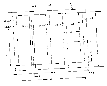
Figure 1 is a planar view of a one-dimension polarization
sensitive infrared detector cell in accordance with the present
invention,
Figure 2 is a section view taken along line 2-2 of a segment
of the infrared detector cell shown in Figure 1,
Figure 3 is a section view taken along line 3-3 illustrating
a group of segments in the infrared detector cell shown in Figure
1,
Figure 4 is a graph of predicted infrared energy absorbance
for detector cell 10,
Figure 5 is a section view of a further embodiment of the
present invention which comprises a modified segment of an infrared
detector cell as shown in Figure 1 with the addition of metal
contacts to the base and cap layers,
Figure 6 is a planar view of a further embodiment of the
present invention which includes transverse segments for a two-
dimension polarization independent design, and
Figure 7 is a graph of predicted infrared energy absorptance
for detector cell 100 shown in Figure 6.
4 OF 28
CA 02141966 1995-02-13
.
Detailed Description of the Invention
A first embodiment of the present invention is illustrated in
Figures 1, 2, and 3. An infrared detector cell 10 functions as a
diffractive resonant optical cavity diode. The cell 10 includes
parallel photovoltaic segments 16, 18, 20, 22 and 24, each
Comprising a plurality of layers as shown in section views in
Figures 2 and 3. The parallel segments 16, 18, 20, 22 and 24 make
up a one-dimensional diffractive grating structure. A transverse
segment 14 interconnects the segments 16, 18, 20, 22 and 24.
The segments 16, 18, 20, 22 and 24 are made up of etched
portions of a conductive layer 28, a base layer 30, a p-n junction
32 and a cap layer 34. The cell 10 further includes a conductive
layer 36 and a passivation layer 46. The characteristics of these
layers are set forth as follows, where the symbol "A" represents
the dimensional unit "angstrom":
ELEMENT THICKNESS MATERIAL
Conductive Layer 28 1,000 A HgTe(conductive semi-
metal)
Base Layer 30 7,000 A HgCdTe (x=.21-.225)
(indium or iodine
doped n-type 10'S/cm3)
Junction 32 5,000 A Graded p-n junction
between layers 30 and 34
Cap Layer 34 15,000 A HgCdTe (x = 0.26-0.3)
(arsenic doped p-type
101'/cm3)
Conductive Layer 36 1,000 A HgTe (conductive semi-
metal)
Passivation Layer 46 1,000 A CdTe (nonconductive)
5 OF 28
CA 02141966 1995-02-13
., _ , __ Mercury. cadmium. telluride . (Hgl_XCdxTe ) is characterized by the
symbol "x" which represents the proportion of Cd to Hg. The
proportion of Hg is represented by "1-x".
The diffractive resonant optical cavity diode as described is
a p-on-n heterojunction diode configuration. Alternative
embodiments include n-on-p heterojunction configuration, or, p-on-n
or n-on-p homojunction configurations. In a homojunction, the base
and cap layer "x" values are the same. In a heterojunction, the
base and cap "x" values are different.
A segment structurally similar to segment 14 is located
beneath conductor 12 and provides the same electrical functions as
segment 14.
.,
An aluminum conductor 12 is a strip of deposited aluminum
which is in electrical contact with the layer 28. Conductor 12 has
a thickness of approximately 500 A and a width of approximately 5
mlcrons.~
The- detector cell 10 shown in Figures 1, 2 and 3 is designed
for receiving in the long wave infrared (LWIR) radiation band,
i.e., wavelengths in the range of 8-12 microns. The uniform
spacing distance of the segments 16, 18, 20, 22 and 24 is defined
as the "period" of the diffractive grating structure and is
represented in Figure 1 by the symbol "A". The period, A, of the
cell 10 is less than or equal to the shortest wavelength in the
radiation band of interest. For this embodiment, A is 8.0 microns.
Using this period, the diffraction of reflected infrared radiation
is suppressed while the diffraction of infrared radiation in the
diffractive resonant optical cavity is promoted. The efficient
6 Ur~ ~ a
CA 02141966 1995-02-13
coupling of diffractive mode energy in the diffractive resonant
optical cavity structure leads to high absorption of infrared
energy. Hence, cell 10 is referred to as a "diffractive resonant
optical cavity" structure. The cavity extend, from the surface of
the reflector layer to the upper surface of the passivation layer.
The width of each of the segments 16, 18, 20, 22 and 24 is
represent in Figure 1 by the symbol "w". The preferred w for these
segments of cell 10 is 1.5 microns.
The overall width of the detector cell .LO is represented by
the symbol "W" in Figure 1. The preferred W for cell 10 is 40
microns. The overall length of the cell 10 is represented by the
symbol "L". The preferred L for cell 10 is 40 microns.
The cap layer 34 is farmed on the surface of layer 36 which is
electrically conductive.
The, conductive layer 36 is formed on the surface of a ground
plane layer 38. The layer 38 comprises deposited aluminum having
a thickness of approximately 500 A. Layer 38 has a reflective
surface 40 which serves to reflect incident infrared radiation
received by cell 10 and forms a highly reflective surface in the
diffractive resonant optical cavity structure. The layer 38 also
serves~as an electrical conductor which is ohmically connected to
the cap layer 34 segments through the conductive layer 36.
An epoxy layer 42 bonds a substrate 44 to the ground plane
layer 38. The epoxy layer 42 has a selected thickness of 10,000 A
and comprises an optical grade epoxy, such as made by Masterbond
Company. The substrate 44, which preferably is 20-40 mils thick,
i yr ~ cs
CA 02141966 1995-02-13
provides a mechanical support for the cell 10 and can comprise, for
example, sapphire or silicon. The substrate 44 may comprise a
silicon integrated circuit. which has circuit components to receive
the detection signal produced at the electrical conductor outputs
(such as 12 and 38) of the cell 10. Such read out integrated
circuits (ROIL) for infrared detectors are shown in U.S. patents
5,179,283 to Cockrum et. al., which issued ~Tanuary 12, 1993 and is
entitled "Infrared Detector Focal Plane", and 4,970,567 to Ahlgren
et al., which issued November 13, 1990 and is entitled "Method and
Apparatus for Detecting Infrared Radiation, Monolithic
Photodetector", and these two issued U.S. patents are incorporated
herein by reference.
The detector cell 10 further includes the passivation layer
46, comprising nonconductive CdTe. Layer 46 is shown only in
i
Figure 3, not Figures 1 and 2, for clarity of illustration.
The distance from the reflective surface 40 to the upper
surface eof the passivation layer 46 is approximately an odd
multiple of the effective wavelength of the incident infrared
radiation in the region between the reflective surface 40 and the
upper surface of the passivation Layer 46. For the present
embodiment, this distance is 3.0 microns which is a 3 factor
multiple of the effective quarter wavelength of approximately 1.0
micron. The effective quarter wavelengt=h is the free space quarter
wavelength (which is 2.5 microns for a detector designed to operate
at a wavelength of 10 microns) divided by the effective refractive
index for this embodiment. The refractive index varies from layer
to layer, but for the structure 10 as a whole, the effective
refractive index is 2.5. This yields the effective quarter
wavelength of 1.0 micron.
8 OF ~ti
CA 02141966 1995-02-13
f
Fabrication of the detector 10 is preferably performed as
follows. The base layer 30, junction 32 and cap layer 34 are
epitaxially grown on a substrate (not shown) of CdTe, CdZnTe, or
GaAs, with the value of "x" and extrinsic doping being changed as
the growing proceeds to produce the layers 30 and 34 and junction
32 as described above.
The conductor layer 36 is deposited or epitaxially grown on
the cap layer 34 and the aluminum ground plane layer 38 is
deposited on the conductor. layer 36.
The device, as thus far produced, is bonded to the substrate
44 by the epoxy layer 42. The substrate (not shown), on which the
layer 30 was grown, is then removed by use of selective etching,
for example, the use of HF, peroxide (H?Oz) and water (H20) , or HN03~
H~OZ and HzO.
The conductor layer 28 is deposited on the base layer 30.
A conventional resist is applied to the layer 28 in the
desired .configuration for forming the diffractive structure
consisting of segments 14, 16, 18, 20, 22, 24 and a corresponding
segment beneath strip 12. Etching is preferably performed by
bromine ethylene glycol aerosol etching or free methyl radical
plasma~etching.
The aluminum conductor 12 is delineated <~nd deposited on the
layer 28 using standard photolithographic lift-off processing.
The detector cell 10 shown in Figures 1, 2, and 3 primarily
absorbs anly one linear polarity of the inc:iden.t infrared radiation
9 OF 28
CA 02141966 1995-02-13
because of the physical configuration of the elongate segments 16,
18, 20, 22 and 24, which receive the incident infrared radiation.
A two-dimension polarity detector cell 100 is described below in
reference to Figure 6.
Referring to Figures 1, 2 and 3, the detector. cell 10 receives
incident, primarily normal, infrared radiation. The detector cell
with the segments 16, 7.8, 20, 22 and 24 functions as an optical
diffraction grating as described in "Analysis and Applications of
Optical Diffraction by Gratings" by Thomas K. Gaylord and M. G.
10 Moharam in Proceedings of the IEEE, Vol. 73, No. 5, May 1985. The
detector cell 10, which includes the reflective ground plane layer
38, operates as a diffractive resonant optical cavity. Incident
infrared radiation is efficiently coupled into diffractive mode
energy in cell 10 and absorbed in the base layer 30 to generate a
photovoltaic current betv:~een t~~e base layer 30 and cap layer 34 in
each of the segments 16, 18, 20, 22 and 24. This current comprises
a detection signal which is conducted through the interconnect
segments of layer 30, including segment 14, t.o the aluminum
conductor 12, and through the r_onductor layer 36 to the conductive
ground plane layer 38. Thus, the detection signal for cell 10 is
produced between aluminum conductor 12 and aluminum ground plane
layer 38. The detection signal for one cell 10 preferably
represents a picture element (pel) within an array of cells 10. A
plurality of such detection signals c:an be used to produce an
image.
The detection signals for each of a group of. cells 10 can be
provided to an ROIC substrate, as noted above, to produce a
composite infrared image.
10 OF 28
CA 02141966 1995-02-13
Figure 4 is a graph representing the predicted quantum
efficiency of the detector cell shown in Figures 1-3. Cell 10 is
optimized for detection in the middle of the 8-12 micron band at
approximately 10 microns.
A second embodiment of the present invention is a detector
cell 60 illustrated in a section view i.n F:igure 5, which
corresponds to the section view in Figure 2. This embodiment is a
modification of the embodiment shown in Figures 1, 2, and 3. Like
reference numerals previously described above refer to like
elements in detector cel.1 60. A passivation layer 37 of CdTe
having a thickness of approximately 1000 A is formed on layer 34.
An aluminum groundplane layer 66 having a thickness of
approximately 1000 A is formed on layer 37 thereby producing a
reflective surface 68 at t:he interface of the layers 37 and 66. ,
A conductive strip 70, preferably aluminum having a thickness
of 1000 A, is formed on and in electrical contact with layer 34.
An aluminum strip 64, having a thickness of 1000 A, is formed on
layer 30.
In detector cell 60, the detection signal. is produced between
the conductive strips 64 and 70.
A'further embodiment of the present invention is a detector
cell 100 shown in Figure 6. Cell 100 is similar t:o cell 10 shown
in Figure 1 but includes added transverse photovoltaic segments,
physically corresponding too the previously described segments 16,
18, 20, 22, and 24. The horizontal and transverse photovoltaic
segments form a rectangular two-dimensional diffraction grating.
11. Vr ~o
CA 02141966 1995-02-13
Detector cell 100 includes vertical- photovoltaic segments 116,
118, 120, 122, and 124 together with intersecting horizontal
photovoltaic segments 130, 132, 134, and 136. Layer 112 is a
similar aluminum layer to layer 12 shown in Figure 1. A
photovoltaic segment 114 corresponds to segment 14 in Figure 1.
The spacing and dimensions of t:he horizontal and vertical segments
in detector cell 100 correspond to the segment spacing in cell 10
shown in Figures 1, 2, and 3.
The detector cell 100 absorbs both horizontally and vertically
polarized infrared radiation and is thus an unpolarized detector.
The detector cell 100 has a cross-sectian configuration
substantially as shown in Figures 2 and 3 and having the following
characteristics (the material is the same as shown in the chart for
detector cell 10):
Element Thickness
Conductive Layer 28 1,000 A
Base Layer 30 7,000 A
Junction 32 5,000 A
Cap Layer 34 15,000 A
Conductive Layer 36 1,000 A
Passivation Layer 46 1,000 A
The predicted spectral quantum efficiency, f:or a 3/4 wavelength
resonance detector cell 100, i.s shown in Figure 7 for a detector
cell, as shown in Figure 6, in which the base layer 30 has x = .21,
and the cap layer 34 has x = .26. The total diode thickness is 3.0
microns. The period A is 7 microns, and the width w is 1.0
microns. The passivation layer 46 in this embodiment is 1000 A.
The effective refractive index for detector cell 100 is 2.5. This
yields an effective quarter wavelength of 1 micron.
12 OF ~~s
CA 02141966 1995-02-13
Referring to Figure 7, it can be seen that the predicted
quantum efficiency exceeds 90~ at the mid-region of the 8-12 micron
band of interest . The detector cell 100 is op t:imized for detection
in the middle of the 8-12 micron band at 10 microns.
The embodiments of the invention described herein involves the
mercury cadmium telluride material system for operation in the LWIR
spectral band. Operation in the LWIR band can also be achieved if
an indium gallium antimonide/indium arsenide or indium antimonide
arsenide/indium antimonide strained layer superlattice material
system is used. The invention can be applied too the mid wavelength
spectral band (3-5 microns) using mercury cadmium telluride, indium
antimonide, indilun gallium antimonide or indium antimonide arsenide
material systems. The invention can also be applied to the short
wavelength spectral band (2-2.5 microns) using the indium gallium
arsenide material system.
The detector cells of the present invention can be scaled for
optimization at selected infrared wavelengths. The detector cell
10 and cell 100 embodiments are opt=imized for use in the 8-12
micron infrared radiation band with peak response in the middle of
the band for approximately 10 micron infrared radiation. The
thickness of the various layers (shown above in charts for cells 10
and 100) can be varied to produce optimizations at other infrared
wavelengths.
The advantage of a photovoltaic diffractive resonant optical
cavity design over a photovoltaic refractive resonant optical
cavity infrared detector and a conventional photovoltaic detector
as described in "Photovoltaic Infrared Detectors" by M. B. Refine,
A. K. Soad and T. J. Tredwell in Semiconductors and Semimetals, Vol
1J ~r ~c~
CA 02141966 1995-02-13
18 , Mercury Cadmium Telluride, edited by R . K . Wi llardson and A. C .
Beer, Academic Fress, 1981, Chapter 6, is that the photovoltaic
diode volume and cross-sectional area are reduced without a
reduction in infrared radiatian absorptance thereby leading to
higher D* performance and increased diode resistance.
Although several embodiments of the invention have been
illustrated in the accompanying drawings and described in the
foregoing Detailed Description, it will be understood that the
invention is not limited to the embodiments disclosed, but is
capable of numerous rearrangements, modifications and substitutions
without departing from the scope of the invention.
14 OF 2$