Note: Descriptions are shown in the official language in which they were submitted.
'- 2142172
. .
Application Of: Jean-Claude Marcou, et al
For: Ground Fault Interrupter Wiring Device and Methods of
Assembly and Testing Thereof
Background Of The Invention
The present invention relates to the class of electrical
wiring devices known as ground fault interrupter (gfi) receptacles
and, more specifically, to novel gfi receptacles suited for fully
automated assembly, and to novel means for and methods of
assembling and testing gfi receptacles.
Receptacles with circuit interrupting capability have come
into wide-spread use in recent years, resulting in concerted
efforts to reduce the cost of parts and labor required for their
assembly while maintaining a high degree of operational
reliability. Automated assembly techniques are widely used today
to reduce labor costs, but at least some operations are still
performed manually in virtually all commercially produced gfi
receptacles.
Certain tests are performed upon gfi receptacles after
complete assembly to ensure proper in-service operation. Some gfi
receptacles have two or more housing sections which are mutually
assembled by releasable connecting means and, following successful
testing, are permanently connected, e.g., by heat fusion of
opposing surfaces. - Permanent connection of the plastic housing
sections by mechanical means such as riveting, while providing
certain advantages, add to assembly costs and are not generally
employed in present-day gfi receptacles. Furthermore, in a
currently conventional manner of fabrication of gfi receptacles,
- 2142~72
certain of the tests performed may not be entirely reliable for the
intended purpose. '
- It is a principal object of the present invention to provide
a gfi receptacle of novel design conducive to fully automated
assembly.
Another object is to provide a novel, fully automated method
of assembly of a gfi receptacle.
A further object is to provide a gfi receptacle having
features which permit testing after complete assembly of all
~ 10 component parts, followed by either permanent assembly in a novel
manner upon successful testing, or disassembly without damage to
any components upon unsuccessful testing.
Still another object is to provide novel and advantageous
means for and method of permanently connecting housing sections of
a gfi receptacle, following complete assembly of all components,
releasable coupling of the housing sections, and performance of all
required tests.
A still further object-is to provide a gfi receptacle
including circuit components mounted on a printed circuit board
having enhanced reliability of testing after assembly.
Yet another object is to provide a novel method of fabrication
of a gfi circuit board which enhances the degree of reliability of
tests designed to detect certain manufacturing defects.
Other objects will in part be obvious and in part appear
hereinafter.
Summary Of The Invention
2142 172
The gfi receptacle of the invention includes a plurality of
components and subassemblies which may be placed in fully assembled
relation by downward, vertical movement in a predetermined
sequence. The parts are uniquely configured to permit assembly in
this manner by fully automated means, thus eliminating costly
manual assembly procedures. The configuration of parts and
sequence of assembly also permit electrical connection of certain
elements without otherwise required soldering.
- Certain subassemblies and individual components are assembled,
all by downward, vertical movement, with the printed circuit board
after attachment thereto of surface-mount-device (SMD) electrical
components. The SMD components-include a pair of jumper cables
which extend between respective pairs of electrical terminals on
the board. One aspect of the assembly method includes breaking
continuity of the usual circuit board traces connecting these pairs
of terminals prior to surface mounting of the jumper cables on the
board. As will be seen, this technique improves the reliability of
operational testing of the gfi device.
Following the soldering operation, the circuit board and
elements previously assembled therewith are moved vertically
downward into the space defined by the rear housing section, the
outer, rear surface of which rests on a horizontal support. After
downward, vertical movement of several other elements into mutually
assembled relation, the front housing section is moved downwardly,
being guided into mating relation with the rear section by a
plurality of posts on the front section which extend through
_ 2-142172
~ I .
openings in the rear section.
At termination of its downward movement the front section is
- releasably attached to the rear section by snap-fit detent means.
The reset and test buttons are then assembled by downward, vertical
movement into respective openings in the front housing section, and
the required electrical tests are performed to ensure proper
operation of the device. If any tests indicate unsatisfactory
operation, the housing sections may be disengaged and the defective
parts replaced or repaired. If the tests indicate proper
operation, the housing sections are permanently joined by
ultrasonic softening and physical deformation of the portions of
the posts on the front section which protrude through the openings
in the rear section. This has the effect of providing a
mechanical-type, permanent connection of the housing sections, with
the deformed ends of the posts being in the nature of rivet heads
without requiring separate rivets and a conventional riveting
operation.
Brief Descri~tion Of The Drawinqs
Figure 1 is a perspective view of a fully assembled ground
fault interrupter wiring device, namely, a duplex electrical
receptacle, embodying features of the invention;
Figure 2 is a top plan view of the front section or cover of
the housing of the receptacle of Figure 1;
Figures 3 and 3a are end elevational views of the front
housing section, as seen from the top and bottom, respectively, of
- Figure 2;
2142172
,, ',;
Figure 4 is a side elevational view of the front housing
section, the appearance being the same from both sides;
. Figure 5 is a bottom plan view of the front housing section;
Figure 6 is a side elevational view in section on the line 6-6
of Figure 5;
Figure 7 is a top plan view of the rear section or body of the
housing of the receptacle of Figure l;
Figures 8 and 8a are end elevational views of the rear housing
section, as seen from the top and bottom, respectively, of Figure
7;
Figure 9 is a side elevational view of the rear housing
section, the appearance being the same from both sides;
Figure 10 is a bottom plan view of the rear housing section;
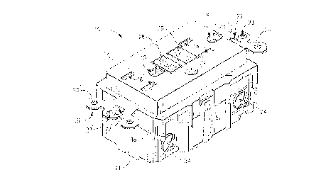
Figure 11 is an exploded perspective view of components of the
GFI device which are configured for automated assembly with the
housing sections;
Figure 12 is a further exploded perspective view of certain of
the components shown in Figure 11;
Figure 13 is a bottom plan view of a printed circuit board,
the top of which is seen in Figures 11 and 12;
Figures 14a and 14b are fragmentary, enlarged, side
-~ . elevational views of portions of Figure 13 illustrating steps in
the fabrication of the device;
Figure 15 is a perspective view of the circuit board and
components mounted thereon assembled within the rear housing
section;
CA 02142172 1997-12-0~
Figure 16 is a side elevational view in section on the line
16-16 of Figure 15;
Figure 17 is an enlarged fragment of Figure 16;
Figure 18 is an enlarged, fragmentary, elevational view, in
section on the line 18-18 of Figure 17;
Figure 19 is a top plan view of a component of the device,
termed a separator;
Figure 20 is a bottom plan view of the separator;
Figure 21 is a side elevational view of the separator;
Figure 22 is a side elevational view in section on the line
22-22 of Figure 19;
Figure 23 is an elevational view in section in the position
of Figure 18, with the separator and other elements in assembled
relation;
Figure 24 is a side elevational view, showing further
elements in assembled relation;
Figure 25 is a top plan view of the elements as shown in
Figure 24;
Figure 26 is a side elevational view in section on the line
26-26 of Figure 25;
Figure 27 is a side elevational view showing the manner of
assembly of the front housing section with the rear housing
section, the latter containing and/or supporting the other
components of the receptacle;
Figure 28 is an end elevational view in section on the line
28-28 of Figure 27, illustrating the manner of releasably securing
VLS:jj 6
''_ 2142172
the housing sections in assembled relation;
Figure 29 is an end elevational ~view in section in the
; positions of Figures 18 and 23 lllustrating the manner of assembly
of the reset mechanism;
- . Figures 30 and 31 are fragmentary, elevational views in
section on the line 30-30 of Figure 29, showing the positions of
the elements with the moveable contacts engaged and disengaged,
respectively, with the fixed contacts;
- -Figure 30a is an enlarged, fragmentary, elevational view in
10 section on the line 30a-30a of Figure 29;
Figure 32 is an elevational view in section on the line 32-32
of Figure 27, illustrating the manner of assembly and operation of
the test mechanism;
Figure 33 is a fragmentary, enlarged elevational view, in
section, illustrating the manner of permanent connection of the
housing sections;
Figures 34 and 35 are perspective views of alternate
embodiments of certain elements;
Figure 36 is a side elevational view of another alternate
embodiment. .
Detailed DescriPtion
-.Referring now to the drawings, in Figure 1 is shown a fully
assembled wiring device 10 typical of the class of devices
embodying the features of the present invention. Device 10 is a
ground fault interrupter (hereinafter abbreviated as "gfi"),
duplex, two-pole, electrical receptacle, although it will be
~_ 2142172
,
understood that certain features of the inventions may be
incorporated in other gfi devices, including circuit breaker types
requiring only one pole or multiphase devices requiring three or
more poles.
As is typical of such devices, components are enclosed in a
space defined by housing means comprising a cover or front section
12 and a body or rear section 14. As will later become apparent,
the front and rear sections are retained in mutually secured
~relation by both releasable and permanent securing means. A first
pair of through openings 16 is provided in front section 12 to
receive a pair of blades of a standard electrical plug, together
- with a third opening 18 for receiving the ground prong of plugs
equipped therewith. A second set of through openings 16', 18' is
provided to accept a second plug.
A metal grounding and mounting strap, denoted generally by
reference numeral 19, includes a central portion, not seen in
Figure 1, disposed within the enclosed space defined by housing
sections 12 and 14, and mounting ears 20, 20' extending outwardly
from opposite ends of device 10. Ears 20, 20' include the usual
openings 22, 22', respectively, for passage-of screws to mount
device 10 in a conventional wall box, as well as threaded openings
23, 23' to receive screws for mounting a conventional wall plate
(not shown). Also seen in Figure 1 are a pair of screws 24, 24'
for electrical connection of the bare ends of conductors on the
line and load sides of the device; as will be seen later, a second
pair of screws are provided for connection of conductors on the
~_ 2142172
opposite side of device 10.
A pair of rectangular buttons 26 and 28, labeled "Test" and
"Reset", respectively, -are-positioned in respective, through
openings 30 and 32 in front housing section 12. Transparent lens
34- covers an opening in front section 12 for viewing of an
operational-indicating LED, as explained later in more detail.
Another feature of particular interëst in connection with front
section 12 is the two rows of four post members each, all indicated
by reference numeral 36, extending rearwardly (i.e., in the
direction of rear housing section 14 in the assembled condition)
along opposite sides-~of the front section. As will be seen, these
post members 36 provide an important function in the final assembly
of device 10.
The appearance of front section 12 is similar at its opposite
ends, as seen in Figures 3 and 3a. The upper end, i.e., the end
adjacent opening 18, includes a pair of notches 38 for
accommodating edges of one of the grounding terminals on the
mounting strap. Edge 40 of end wall-42 mates closely with a
corresponding end wall edge of rear section 14, and open area 44
provides access to the screw for connecting the bare end of a
ground wire to a depending tab on mounting strap 19, as seen later.
Edges 46 of wall portions 48 at the lower end mate closely with
corresponding edges of rear section 14.
- Circular wall portion 50 surrounds the previously mentioned
2S LED in the assembled condition. Tapered lugs 52, 52' extend
outwardly from central portions of the outer surfaces on opposite
21g217~ .
of the front housing section. Lugs 52, 52' provide stepped
shoulders 54, 54' and taper inwardly to-~meet surfaces 56, 56' at
- the edge which mates with rear section 14. Circular wall portions,
termed towers and denoted by reference numerals 58, 58' extend
rearwardly from the inside of the front wall of front section 12 to
provide abutment means for a pair of coil springs described
hereinafter.
Rear housing section 14 is shown in greater detail in Figures
7-lO. As in the case of front section 12, rear section 14 is
preferably formed as a unitary, molded plastic part. The rear or
outer surface of rear section 14, i.e., the surface which is
exposed in the assembled condition, is seen in Figure 7, and the
inner surface, which forms a portion of the enclosed space defined
by the assembled housing sections, is seen in Figure 10. Through
openings 36' in portions 37' of rear sections 14 are positioned
complementary to posts 36 of front section 12 so that, as the front
and rear sections are moved linearly into mating engagement, posts
36 pass through openings 36'. During such relative movement of the
housing sections, tapered lugs 52, 52' on front section 12
outwardly deflect resilient tabs 53, 53' on rear section 14 until
stepped shoulders 56, 56' on the lugs clear edges 55, 55' of
- openings 57, 57' in tabs 53,- 53'. When this occurs, the natural
resilience of tabs 53, 53' causes them to return to their original
positions, wherein stepped shoulders 56, 56' abut edges 55, 55' of
openings 57, 57'. The housing sections are thus retained in mating
engagement by the snap fit means of the lugs and tabs, such
2142172
,
engagement being releasable by using a tool to deflect tabs 53, 53'
outwardly to permit passage of lugs 52, 52' past edges 55, 55'.
- - When the housing sections are in mutually mating engagementj
opposing edges of side and end wall portions thereof abut one
5 - another to provide essentially full enclosure of the space wherein
the other elements of gfi device 10 are positioned. For example,
edge 40 at the upper end of front housing section 12 (Figure 3)
abuts edge 40' of rear section 14 (Figure 8), and edge 41' borders
previously mentioned open area 44. Likewise, edges 46 at the
opposite end (Figure 3a) abut edges 46' (Figure 8a) and end wall
portion 47 of rear housing section 14 fills the space between these
abutting edges. Through openings 59 are provided for passage of
the ends of conductors to be connected to terminals within the
housing, as explained later.
All of the elements which are positioned within the enclosed
space defined by housing sections 12 and 14, including the
previously mentioned mounting strap 19, test button 26 and reset
button 28, are shown in exploded, perspective view in Figure 11.
Further details of construction, assembly and operation of the
elements will be provided later herein, but identification of the
elements and a general understanding of their interrelationship is
facilitated by Figure 11. Printed circuit board 60 provides a
support for solid-state components of the gfi circuitry and
includes the usual copper traces interconnecting the components in
the required manner. In addition to the electrical and electronic
components, certain sub-assemblies are mounted upon board 60.
21421~72
,
.
Solenoid coil 62 is wound on a hollow core portion of plastic
support element 64 and stem 66a of moveable solenoid armature 66,
- having enlarged head portion 66b, passes loosely through this
hollow core. Cylindrical plastic housing 68 and circular plastic
cover 70 provide an enclosure for a pair of toroidal cores 72 and
associated windings used in sensing an imbalance in current flow
through the hot and neutral conductors of device 10 in the usual
manner of gfi devices. Wall 74 is formed integrally with cover 70
- and provides a dielectric separator for upper portions 75a, 76a of
a pair of conducting posts or strips 75, 76, respectively, which
extend through openings in cover 70 and through cores 72. Forward
portions 75b, 76b of strips 75, 76, respectively each carry a fixed
contact through which the circuit of the hot and neutral lines is
completed. Thus, strips 75 and 76, including their upper and
forward portions, form parts of the hot and neutral conductors of
the circuit in which gfi device 10 is connected.
Sheet metal member 78, termed a latch spring, has an abutment
portion 78a at one end, leaf spring 78b at the other end, and
opening 78c in an intermediate portion. When assembled, the U-
shaped end of spring 78b extends into a cavity of support element64, and abutment portions 78a is positioned for contact by the free
end of solenoid armature stem 66a. Buss bars 80, 81 are supported
on opposite, upper sides of latch block 82 with integral posts 82a,
82a' of the latch block extending through openings 80a, 81a,
respectively, to provide positive location of the buss bars on the
latch block. Buss bar 80 carries spaced contacts 80b and 80c; buss
2142172
.,
bar 81 carries spaced contacts 81b and 81c.
An integral, molded, plastic part, termed a separator and
indicated generally by reference numeral 84, -includes a plurality
of wall portions and openings, the locations and purposes of which
are described later. Portions of separator 84 support and
laterally constrain mounting strap 19 which is seen in Figure 11 to
include rivet-connected ground contacts 85, 85' for receiving the
grounding prongs (extending through openings 18, 18') of electrical
plugs connected to device 10. Depending tab 87 has a threaded
opening for screw 87' to connect a ground wire to strap 19.
Openings 86 and 88 in strap 19 are provided for passage through the
strap of pins on test button 26 and reset button 28, respectively.
Pin 26a is integrally formed in the plastic molding of button 26,
and metal pin 28a, having shoulder 28b, is fixedly secured to the
plastic molding of button 28. Coil spring 89 encircles stem 28a
and has a diameter small enough to pass through opening 88.
Load terminals 92 and 94 are mounted within the housing for
connection thereto of the hot and neutral conductors, respectively,
on the load side of device 10. Such connection of the neutral
conductor may be made to terminal 94 by inserting a bare end of the
conductor through either of an appropriate pair of openings 59, and
between depending tab 94a of terminal 94 and pressure plate 94a';
screw 24' passes through an open-ended slot in tab 94a and a
threaded opening in plate 24a', and is tightened to provide good
electrical contact between the conductor and terminal. The hot
conductor on the load side is similarly connected to terminal 92 by
' 2142172
. .
another screw and pressure plate, not shown in Figure 11. Such
connections are known as "back-wiring".~ The connections may be
alternately made by looping the conductor around the screw between
the screw head and the terminal tab. Female contacts 92b and 94b
are positioned to receive the blades of an electrical plug
extending through openings 16' in front housing section 12, and
contacts 92c, 94c are positioned to receive the blades of a plug
extending through openings 16.
Line terminals 96 and 98 are fixedly connected to circuit
board 60 by posts on the terminals extending through openings in
the board, and soldered to terminals on the lower side of the
board. As best seen with respect to terminal 96, an apen-ended
slot is provided to receive screw 24, with the head of the screw on
one side of the terminal and pressure plate 24a on the other side.
A bare end of the neutral conductor on the line side of device 10
may be back-wired by inserting through one of openings 59, between
plate 24a and terminal 96 and tightly urged against the terminal by
tightening the screw. The hot conductor on the line side is
connected to terminal 98 in like fashion.
Coil springs 97 and 97' pass through respective openings in
separator 84 and are compressed between buss bars 80 and 81, and
- towers 58, 58' on the interior of front housing section 12 when
device 10 is fully assembled, as described later. Test blade 100
includes laterally and forwardly extending legs lOOa and lOOb,
respectively, a medial portion of the blade being positioned for
contact by pin 26a upon depression of test button 26. LED 102 is
CA 02142172 1997-12-0~
positioned within the housing for viewing through previously-
mention lens 34; electrical leads 102a extend from opposite sides
of LED 102, with voltage-dropping resistor 102b interposed in one
lead, for connection in the circuit in a manner later described.
Circuit board 60 and elements mounted thereon are shown in
more detail in Figures 12-14. Opposite surfaces 60a and 60b or
board 60 are seen in Figures 12 and 13, respectively. A plurality
of surface-mount-device (SMD) electronic components are attached
by a suitable adhesive to surface 60b at positions interconnected
by preformed copper traces on board 60 to provide portions of the
gfi circuitry. Although the circuitry itself is conventional, and
therefore not described in detail by way of electrical schematics,
or the like, a unique feature is provided by a fabrication
technique relating to jumper cables 104, 104' and related portions
of the circuit, as shown in Figures 14a and 14b.
Cable 104 connects terminals 104a and 104b, and cable 104'
likewise connects terminals 104a' and 104b'. Cables 104, 104' are
preferably formed by flattening initially round sections of
electrical wire on at least one side to provide a flat surface for
adhesion to the board by glue dots 105 (Fig. 14b). As is the
usual practise in construction of circuit boards for gfi devices,
terminals 104a and 104b are connected by a copper trace 104c,
terminals 104a' and 104b' being likewise connected. The reason
for also connecting these terminals via jumper cables is to carry
relatively high currents between these terminals.
In the present gfi device, trace 104c and the trace
connecting
VLS:jj 15
~ ~142172
terminals 104a' and 104b' are broken, as indicated at 104d, prior
to mounting of jumper cable 104. This provides an important and
- useful function in testing the circuitry of device 10. Standard
operational testing of device lo is intended to reveal the presence
5 or absence of circuit continuity through the jumper cables, the
device being rejected as defective if, for example, one or both
cables are inadvertently omitted or defectively connected to the
terminals. In conventional devices it is possible that the traces
may carry the current for the relatively short interval of testing,
10 - thus indicating an operative device even though the jumper cables
are omitted or defectively connected. The traces are then likely
to be blown out by longer application of higher currents during
normal, in-service operation of the device. This problem is
obviated by the technique of fabrication of gfi device 10 since
only the jumper cables can carry current between the terminals.
one of the ends of the wire of coil 62 is connected to
conductive pin 62a which extends rigidly from support element 64
through an opening in circuit board 60 for solder connection to the
circuit on surface 60b. The other end of the coil wire is
connected to a conductive pin which is hidden in Figure 12, but
which extends through opening 62b in board 60. Short posts 64a,
integral parts of the plastic molding of element 64, also extend
through openings in board 60, as does lower end 106a of a
conductive pin which is physically incorporated in element 64
during the molding operation and solder-connected in the circuit on
surface 60b. Upper end 106b of this pin extends through separator
142172
84 upon final assembly for contact by test blade leg lOOb during
in-service testing of device 10, as described later.
Integral posts 96a and 98a extend from line terminals 96 and
98, respectively, through openings in board 60, as does post 98b of
5terminal 98 and a corresponding post (not seen) of terminal 96, the
latter posts being solder-connected to respective ends of jumper
cables 104, 104'. Block 68a is an integral part of the plastic
molding which includes cylindrical housing 68. The lower ends of
four pins which are molded into block 68a, and to which the ends of
10the windings on cores 72 are respectively connected, extend through
openings in board 60 for respective connection on surface 60b. The
two leads of movister 107, three leads of SCR 108, and the two ends
of the conductor carrying resistor 110, likewise extend through
openings in board 60 for connection in the circuit on surface 60b.
15The preferred manner of automated manufacture of device 10
begins with adhesion of the SMD components in their proper
positions on surface 60b, with this surface facing upwardly.
Continuity of trace 104c and the trace (not shown) connecting
terminals 104a' and 104b' is broken, as previously described, and
20SMD jumper cables 104, 104' are adhered by glue dots 105 to surface
60b. After sufficient curing of the adhesive, board 60 is
mechanically flipped over so that surface 60a faces upwardly.
The so-called bobbin and toroid-housing subassemblies are
separately fabricated. The bobbin subassembly is prepared by
25winding coil 62 on the hollow core portion of plastic support
element 64, solder-connecting one end of the coil wire to pin 62a
21~2172
,
and the other end to the pin which, after assembly, extends through
circuit board opening 62b. Armature stem 66a is not inserted
through the core which is surrounded by coil 62 until later in the
operation, as appears hereinafter. Pin 62a, the pin to extend
5through opening 62b, and a pin having opposite ends 106a and 106b
are molded or press fitted into plastic support element 64. The
toroid-housing subassembly is prepared by inserting pre-wound
toroidal cores 72 into housing 68, attaching the ends of the
- windings to the pins in block 68a, placing cover 70 (with integral
10wall 74) on and affixing it to housing 68, and inserting conducting
strips 75, 76 through the openings in cover 70, through toroids 72
in housing-68 and affixing upper portions 75b, 76b to cover 70 on
opposite sides of wall 74 (e.g., by ultrasonic welding of plastic
posts extending through openings in portions 75b, 76b to cover 70).
15With surface 60a facing upwardly, automated assembly proceeds
with downward, vertical movement of movistor 107, SCR 108 and
resistor 110 (in any desired sequence) to insert the respective
leads thereof through the aligned openings in board 60. Armature
stem 66a is mechanically advanced in a horizontal direction through
20the plastic core surrounded by coil 62 to complete the bobbin
subassembly which is then moved vertically downward to insert posts
64a, pin 62a and the other coil wire pin, and pin 106a through the
respective, aligned openings in the circuit board. Latch spring
78, latch block 82 and buss bars 80, 81 are then assembled, in that
25order, by successive, vertical, downward movement of each into
their positions of mutual assembly, best seen in Figures 16-18.
18
CA 02142172 1997-12-0~
The toroid housing subassembly is then moved vertically
downward to insert each of the lower ends of conducting strips 75,
76 and the lower ends of the four pins in block 68a through
aligned openings in circuit board 60. Integral posts 96a, 96b,
98a and 98b on line terminals 96, 98 are then inserted through
openings in board 60 aligned therewith by vertical, downward
movement of the line terminals each carrying one of screws 24 and
plates 24a in the open slot thereof. This is followed by a
soldering operation, connecting all components, leads, pins,
terminals, etc. in the required locations on surface 60b of board
60.
In the next assembly step, rear housing section 14 is placed
with its rear (outer) surface facing downwardly, supported on a
horizontal surface. Circuit board 60, carrying all of the
elements previously assembled as just described, is moved
vertically downward, into the space surrounded by the side and end
walls of rear section 14, as shown in Figure 15. The outer
periphery of board 60 and the inner periphery of the cavity
defined by rear section 14 have complementary configurations to
provide close positional constraint of the board. As seen in
Figure 16, edge portions of board 60 are supported on shoulders
112 within housing section 14, providing clearance for the SMD
components on surface 60b.
Separator 84 is next added to the assembly by vertical,
downward movement to position horizontal wall 84' in essentially
fully covering relation to the elements previously positioned
within rear housing section 14. Details of separator 84 are seen
VLS:jj 19
2142172
in Figures 19-22. Through openings 114, 116 and 116' are mutually
aligned on a laterally extending axis of-~separator 84. Upper end
106b of the test pin extends through opening 117 upon placement of
the separator. A first pair of slots 118, 118', one on each
lateral side of the separator, fit closely around vertically
extending shoulders 119, 119' (Fig. 10), respectively, on the
interior of rear housing section 14. A second pair 120, 120l and
a third pair 122, 122' of separator 84, provide clearances for
portions of terminals 92 and 94 during assembly thereof, as
explained later. Other, unnumbered wall portions on the upper
(Fig. 19) side of separator 84 provides guides and supports for
terminals 92 and 94.
Cavities 124, 124' are surrounded by wall portions integral to
separator 84 along the longitudinal centerline thereof.
Cylindrical wall -126 provides a cavity for placement of LED 102.
Longitudinal cavity 128 on the lower (Fig. 20) side of separator 84
accepts the upper portions of contact strips 75, 76 and wall 74.
A first pair of tabs 130, 130', one on each lateral side, extend
downwardly from wall 84', as does a second pair of tabs 132, 132'.
Upon placement of separator 84, tabs 130, 130' extend along and
provide support for one side of line terminals 96 and 98,
respectively, while tabs 132 and 132' extend into the open, upper
ends of the slots in the line terminals to define, together with
the closed ends of the slots, essentially circular openings
surrounding screws 24. Wall portions 136 extend upwardly on
opposite sides of portions of horizontal support surfaces 137.
' 2142172
With separator 84 in place, LED 102 is moved vertically
downward into the cavity defined by wall 126, with leads 102a
extending-laterally outwardly on opposite sides thereof. Test
blade 100 is then moved vertically downward into position on
- 5 separator 84. Load terminals 92 and 94 are next moved vertically
downward into assembled relation with the separator and other
previously assembled elements. During downward movement of the
terminals, arms 92e and 94e pass through slots 120 and 120',
~ respectively, and tabs 92d and 94d pass through slots 122 and 122',
respectively, as is evident from Figure 25. Leads 102a are firmly
engaged between edge portions of the load terminals and the upper
surface of wall surface 84', thereby connecting LED 102 across the
load side of device 10 without the need for soldered connections of
leads 102a. Also, leg lOOa of test blade 100 is engaged between
terminal 92 and wall 84', as appears later.
Coil springs 97 and 97' are then moved vertically downward
into separator openings 116 and 116', respectively, so that the
lower ends of the coils rest upon central portions of buss bars 80
and 81, and surrounding posts 82a and 82a', as seen in Figure 23.
The sequence of assembly of load terminals 92,-94 and coil springs
97, 97' may be reversed, if desired.
Next, mounting strap 19 is moved vertically downward to rest
upon separator support surfaces 137, the strap being laterally
constrained- by wall portions 136. The elements are now in the
positions shown in Figures 24, 26, wherein it will be noted that
cavities 124 and 124' lie directly beneath ground contacts 85 and
21 12172
85', respectively, being thus positioned to accept the ground
prongs of electrical plugs connected to-~evice 10.
Front housing section- 12 is then positioned above the
previously assembled elements, as shown in dotted lines in Figure
27, and moved vertically downward to the solid line position.
During such movement, each of posts 36 passes through a
corresponding opening 36', and integral tabs 53 and 53' on rear
housing section 14 are deflected outwardly by tapered lugs 52 and
52', respectively, on front section 12. When the front and rear
housing sections are fully engaged, they are releasably secured to
one another by the snap-fit means of lugs 52, 52' and resilient
tabs 53, 53', as previously described. The engagement of lugs 52,
52' under edges 55, 55' of openings 57, 57' of tabs 53, 53' is
clearly seen in Figure 28.
Spring 89 is moved vertically downward along its longitudinal
axis, through openings 32 and- 88 in front housing section 12 and
mounting strap 19, respectively, until its lower end rests upon the
portion of separator 84 surrounding opening 114, as seen in Figure
29. It will also be noted from this Figure that in the mutually
assembled relation of the front and rear housing sections, the free
ends of towers 58 and 58' bear against the upper ends of coil
springs 97 and 97', respectively, thus compressing the springs
between fixed towers 58 and 58' at their upper ends and moveable
buss bars 80 and 81 at their lower ends.
Reset button 28 is then moved vertically downward to extend
-stem 28a through springs 89, as indicated in dotted lines in Figure
22
214~172
29. It will be noted from this and other Figures that integral,
resilient tabs 28c, 28c' are positioned in openings in opposite end
walls of button 28. Tabs 28c, 28c' are integral with the end walls
of the button along the lower sides of the openings and have outer
surfaces which taper outwardly toward the top of the button. The
dimensions of button 28, 28c, 28c' and opening 32 are such that the
tabs are deflected inwardly by the edges of the opening as the
button is moved downwardly. When the stepped shoulders at the free
- ends of tabs 28c and 28c' have cleared the lower edges of opening
32, the natural resilience of the tabs moves them back to their
normal, outward positions and button 28 is captured within openings
32.
As reset button 28 is inserted, the free end of stem 28a,
after passing through spring 89,-opening 88 in strap 19, and
opening 114 in separator 84, passes through opening 82b in latch
block 82 and opening 78c in latch spring 78, extending into cavity
64b of support member 64. Spring 89 biases reset button 28 toward
upward movement which is limited by contact of the free ends of
tabs 28c, 28c' with the internal surface portions of housing
section 12 adjoining the ends of opening 32.
To place the elements of device 10 in normal operating
position, button 28 is manually depressed to move shoulder 28b past
the edge of latch spring 78 which adjoins opening 78c. During this
movement, latch spring 78 will be moved slightly toward the right,
as viewed in Figure 30, compressing leaf spring 78b within its
cavity in support member 64. When shoulder 28b moves below latch
2142172
,
spring 28, the latter is moved back toward the left by the biasing
force of leaf spring 78b and the reset button stem is engaged with
the latch spring.
When manual pressure is removed from reset button 28, spring
89 moves the button back in the upward direction. Due to the
engagement of shoulder 28b with latch spring 78, the latter is also
moved upwardly, together with latch block 82 and buss bars 80 and
81. This further compresses coil springs 97 and 97', meaning of
course that the-biasing force of spring 89 exceeds the combined
biasing forces of springs 97 and 97'. Upward movement of the
elements places contact 80b on buss bar 80 in engagement with
contact 92f on the lower side of load terminal arm 92e, and contact
80c in engagement with contact 75c on the lower side of portion 75b
of line contact 75, as shown in Figure 30. Of course, contacts 81b
and 81c of buss bar 81 are also moved into engagement with
corresponding contacts on load terminal 94 and line contact 76.
When the contacts are so engaged, the free ends of reset button
tabs 28c are spaced from (below) the opposing, internal surface
portions of front housing section 12. Thus, electrical
communication between the line and load sides of device 10 is
established for both the hot and neutral conductors through buss
bars 80 and 81.
Figure 30a illustrates in greater detail the configuration of
the upwardly facing surfaces of latch bloc~ 82 upon which bias bars
80 and 81 are carried. It will be noted that the surface beneath
buss bar 80 slopes downwardly from the center toward each end.
24
~142172
~ .
Thus, the lower surface of the buss bar is supported essentially
only across the mid-point between the posîtions of contacts 80b and
80c. This configuration ensures that both of the moveable contacts
will be fully engaged with the fixed contacts, compensating for any
- 5misalignment which might occur due to opposing planar surfaces
being non-parallel.
An imbalance in current flow through the hot and neutral
conductors is sensed by toroidal cores 72 and their associated
windings. Through the operation of conventional gfi circuitry, the
10current imbalance energizes coil 62, moving armature 66 and latch
spring 78 toward the right. Contact of the free end of stem 66a
with abutment portion 78a moves latch spring 78 to the right, from
the position of Figure 30 to the position of Figure 31, compressing
leaf spring 78 and disengaging the latch spring from shoulder 28b
15on reset button stem 28a.
Upon disengagement of latch spring 78 and shoulder 28b, spring
89 moves reset button 28 upwardly until the free ends of tabs 28c
contact internal surface portions of housing section 12 on opposite
sides of opening 32. At the same time, the biasing forces of coil
20springs 97 and 97' move buss bars 80 and 81 downwardly, moving both
contacts of both buss bars out of engagement with the corresponding
- line and load terminal contacts, thereby deenergizing coil 62,
allowing armature 66 and latch spring 78 to return to their
positions of Figure 30. As shown in Figure 31, both contacts 80b
and 80c are spaced from contacts g2f and 75c, respectively. Thus,
circuit continuity between the line and load sides of device 10 is
2142172
interrupted by a ground fault or other potentially dangerous
condition. The elements may be returned to their positions of
normal operation by manual depression of reset button 28, as
previously explained.
After (or before, if desired) reset button 28 is assembled
with device 10, test button 26 is moved vertically downward, into
opening 30, as seen in Figure 32. Resilient tabs 26b, 26b' in
opposite end walls of test button 26 are deflected inwardly as the
button is inserted and return to their outer positions to capture
- the button in opening 30 in essentially the same manner as tabs
28c, 28c' on reset button 28. Leg lOOa of blade 100 is firmly
engaged between an edge of load terminal 92 and the upper surface
of separator wall 84', as previously mentioned.
Blade 100 is constructed of electrically conducting, springy
sheet metal in a configuration such that it assumes the position
shown in dotted lines in Figure 32. In this position, a medial
portion of blade 100 contacts stem 26a and maintains button 26 in
its dotted line position, with the free ends of tabs 26b, 26b'
contacting the internal surface portions adjacent the ends of
opening 30 in housing section 12. Manual depression of button 26
moves test blade 100 to the solid line position of Figure 32,
bringing leg lOOb into contact with pin end 106b and placing the
pin in electrical communication with terminal 92. This has the
effect of simulating a fault in the line and, if device 10 is
operating properly, results in the previously described operation
to interrupt the circuit. Upon removal of manual pressure from
26
-~ 2142172
,
test button 26, the parts return to the dotted line positions of
Figure 32 and reset button 28 may be depressed to restore circuit
continuity in the manner previously described.
After placement of the reset and test buttons, assembly is
complete and device 10 is ready for testing. Such tests are
standard in the industry although some variations may be employed.
Wires are connected, via the four screws exposed on the exterior of
the device, to the hot and neutral terminals on both the line and
load sides. The normal operating voltage of the device (e.g., 120
Vac) is applied to the line terminals, first with a fault current
slightly below the intended actuating level, and then with a fault
current slightly exceeding that level, which should result in non-
actuation and actuation, respectively. These tests are repeated at
full load, and other tests, e.g., for grounded neutral actuation,
noise voltage non-actuation, and acceptable actuating time upon
application of a 500 ohm ground fault are also performed.
If device 10 fails any of the prescribed tests, it may be
disassembled by removing the releasable connection of housing
sections 12 and 14 in the manner previously described to repair the
defect. If testing is satisfactory, the housing sections are then
permanently connected to one another by ultrasonic deformation of
the free ends of posts 36 of front section 12 which extend through
openings 37' of rear section 14. This has the effect of creating
a mechanical, riveted connection between the housing sections with
enlarged portion 36a acting as a rivet head, as shown in Figure 33.
While the previously described configurations, relative
27
'- ~142172
positioning and manner of assembly of the elements represent the
presently preferred embodiment, it will be understood that
variations in certain details are possible within the scope of the
invention. Examples of some of the many possible variations are
illustrated in Figures 34-36. As shown in Figure 34, leaf springs
80d are attached to (or formed integrally with) buss bar 80.
Springs such as leaf springs 80d would replace coil springs 97, 97'
and provide the biasing force for movement of buss bars 80, 81 to
break circuit continuity. Figure 35 shows an end portion of latch
spring 78 carrying coil spring 78d, which would replace leaf spring
78b and provide the biasing force for latch spring 78. Rather than
compressing coil spring 97, 97' (or springs substituted therefor)
between the buss bars and interior portions of front housing
section 12, such springs could be compressed between the buss bars
and portions of the separator. In any case, all parts are so
configured thatj after separate preparation of bobbin and toroid
housing subassemblies, device 10 may be assembled by fully
- automated means since all parts are placed in assembled relation by
downward, vertical movement.
Coil spring 140 is added in the Figure 36 modification to
maintain the terminal end of solenoid armature 66 in spaced
relation to abutment portion 78a of latch spring 78 when coil 62 is
deenergized. All components other than coil spring 140 have the
same construction, positional relationships of operation as
previously described. Coil spring 140 is weaker than leaf spring
78b of latch spring 78 ~hereby, upon energization of solenoid coil
28
2142172
62, armature 66 moves to compress spring 140 before contacting
abutment portion 78a. This has the advantageous effect of
increasing the momentum of armature 66 prior to contact thereof
with the latch spring, thereby improving the circuit-interrupting
operation of device 10. Without spring 140, the end of armature 66
may be in contact with abutment portion 78a before energization of
coil 62, depending upon the physical orientation of device 10.
Thus, the improved performance provided by inclusion of spring 140
may offset the increase in cost occasioned thereby.
From the foregoing, it may be seen that the present invention
provides a gfi wiring device having components configured for
; mutual assembly, and a method of assembly of a gfi wiring device,
in a manner involving only sequential movement of components and
subassemblies along parallel, straight-line paths. Thus, the gfi
device and assembly method are eminently suited for employment of
fully automated assembly means. The design and operation of such
robotic-type, automated assembly means, requiring only parallel,
linear movement of parts, is within the purview of those skilled in
the art. The invention further provides a gfi device which may be
operationally tested after completion of assembly, and methods of
assembly and testing, with novel and improved means for permanently
- connecting initially separate sections of the device housing
following successful testing, as well as improving reliability of
testing.
29