Note: Descriptions are shown in the official language in which they were submitted.
~a~~~~~~a
1
Method for manufacturing of a mu tilayer microwave board
arid boards obtained on the basis of this method
The invention relates to a method for manufacturing a
multilayer microwave board in which individual layers of
plated laminate can be provided with a conductor pattern
and in which, in a repeated process, individual layers or
semimanufactures are subsequently bonded or provided with
holes, which holes are then plated for realizing
connections between the separate conductor patterns.
The invention also relates to a multilayer microwave board
comprising a bonded package of laminate provided with
conductors and plated layers and with connections between
the conductors in the form of plated through-holes.
The invention furthermore relates to a method for tuning a
multilayer board provided with blind or buried vies.
Both multilayer microwave boards and related manufacturing
methods are well-known in the art. Nevertheless, their
field of application is limited owing to the expensive and
time-consuming production and the high ratio of rejects.
Moreover, several restrictions apply, particularly with
respect to the realization of connections between the
various conductor patterns, the so-called vies. Various
types of connections that are possible in the manufacturing
of conventional multilayer printed circuit boards, cannot,
or only at a high ratio of rejects, be realized. Especially
the production of blind vies, buried vies and sequential
blind vies presents difficulties and the manufacturing of
interlocked vies is even considered to be impossible. Also
microwave multilayers comprising more than three layers are
practically non-existent.
2
The present method according to the invention is aimed at
obviating these difficulties by the application of a simple
and excellently reproducible method and is characterised in
that the multilayer microwave board can be produced in one
operation during which all layers are simultaneously bonded
together to form a multilayer, which multilayer is
subsequently provided with holes, which holes are then
plated after which any excess plating is removed.
The multilayer microwave board according to the invention
is characterised in that the holes penetrate the entire
package and are at least substantially plated between the
conductor patterns to be connected.
The method for tuning a multilayer microwave board
manufactured according to a method well-known in the art is
characterised in that after the actual production of the
board a hole is drilled to at least one buried via in the
board between a stripline and a plated hole, such that this
connection is at least substantially ohmic in nature.
According to the known method, individual layers of plated
laminate are provided with a conductor pattern and, where
necessary, drilled after which the resulting holes are
plated. These layers are then bonded under high pressure
and temperature conditions. By repeatedly bonding the thus
obtained semimanufactures and again drilling and plating
the resulting holes, it is possible to realize more complex
products.
Products realized on the basis of said known method are
characterised by a high ratio of rejects, particularly
since connections between the conductor pattern and plated
holes fail at the high temperature and pressure required
for the bonding process. This is particularly due to
3
fluctuations in coefficients of expansion between metal
parts and the laminate, although the high pressure and
temperature also render the laminate viscous as a result of
which any asymmetry surrounding a plated through-hole may
cause a crack.
In the new, inventive method this problem is not
experienced. It is further characterised in that the holes
are provided by drilling right through the bonded package.
Subsequently the holes are fully plated in a way known in
the art after which any excess plating is mechanically
removed, for instance by means of a drill.
A most favourable embodiment of the method is characterised
in that a diameter of the drill is selected depending on
the type of laminate and on the diameter of the plated hole
in order to obtain optimized wave properties of the
connection between the conductor pattern and the plating at
that position. A favourable selection would for instance be
a diameter of approximately 1,15 times the diameter of the
plated hole.
A further favourable embodiment of the method is character-
ised in that the excess plating, depending on the type of
laminate and the diameter of the plated hole, is removed in
axial direction such that the wave properties of the
connection between the conductor pattern and the plating at
that position are optimized. It may then be effected that
the connection at that position is at least substantially
purely ohmic. A favourable implementation of this method,
using a standard type of laminate of for instance 3/100
inch is characterised in that a volume of excess plating is
retained in axial direction at a length of 10-50 meter.
CA 02142178 2006-05-30
24005-192
4
Since excess plating is mechanically removed in a
multilayer microwave board according to the invention, the
board is further characterised in that the holes, where the
plating has been mechanically removed, have a larger
diameter than the plated holes.
Depending on the type of laminate and the diameter
of the plated hole, the larger diameter can be again
selected such as to yield favourable wave properties of the
connection between the conductor pattern and the plating at
that position, using a standard laminate of 3/100 inch, for
instance approximately 1,15 times the diameter of the plated
hole.
A still further favourable embodiment of the
multilayer microwave board according to the invention is
furthermore characterised in that, depending on the type of
laminate and the diameter of the plated hole, the plating
between the conductor patterns to be connected extends at
least slightly further in axial direction than merely the
distance between these conductor patterns in order to obtain
optimized wave properties of the connection at that
position, for instance over 10-50 meter.
In one broad aspect, there is provided a method
for manufacturing a multilayer microwave board from
individual layers, of plated laminate, each provided with a
conductor pattern or a ground plane, comprising the steps of
bonding the individual layers together, forming holes
through the layers at locations where connections between
separate conductor patterns are desired, plating the holes
to form the connections, removing excess plating from the
holes up to a predetermined depth and a predetermined
diameter, thereby tuning the connections between the
CA 02142178 2006-05-30
24005-192
4a
conduction patterns to minimize reflections of the
connections.
The method of manufacture and the multilayer
microwave board according to the invention will now be
described with reference to the following figures, of which:
Fig. 1 schematically represents the conventional
construction of a multilayer microwave board provided with a
blind via;
Fig. 2 schematically represents the construction
according to the invention of a multilayer microwave board
provided with a blind via.
zi~~~~8
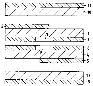
Fig. 1 shows the various steps in a possible manufacturing
process for a multilayer microwave board according to the
state of the art. In Fig. lA, laminate 1, for instance
duroid, is provided with a conductor pattern 2 and a ground
5 plane 3. Laminate 4 is also provided with a conductor
pattern 5 and a ground plane 6. A connection with
favourable microwave properties shall be effected between
conductor pattern 2 and conductor pattern 5. The ground
planes are thereto provided with circular recesses 7, 8,
usually obtained by means of etching. Subsequently, ground
planes 3, 6 are bonded together after which a through-hole
9 is drilled through the package, which is then provided
with a plating according to a method known in the art, as
shown in Fig. 1B. As shown in Fig. iC, laminate 10 provided
with ground plane 11 and laminate 12 provided with ground
plane 13 are then bonded to the package. These bonding
treatments that take place under high pressure and
temperature conditions, may impair the connection between
conductor patterns 2 and 5. Particularly in case of complex
multilayer microwave boards incorporating many connections
and requiring many operations, a faulty connection is
likely to occur. The connection thus effected between
conductor patterns 2 and 5 is moreover found to possess
less favourable wave properties. The transition from a
stripline mode in conductor pattern 2 to a coaxial mode
between plated hole 9 and recesses 7, 8 and subsequently in
a stripline mode in conductor pattern 5 is found to cause
reflections. Even a careful selection of all contributory
components, such as hole diameter, plating thickness and
diameter of recesses 7, 8, still yields a minimum
reflection of -20 dB, which limits the range of application
of the multilayer microwave board.
The known method of manufacture allows several variations
that are of minor relevance. It is for instance possible to
6
leave out ground plane 3 or ground plane 6 or to replace
laminate 10 or laminate 12 by a thick adhesive layer as
well-known in the art. This does not substantially change
the complexity of the process, the ratio of rejects and the
microwave properties.
Fig. 2 shows the simplified method of manufacture of a
multilayer microwave board according to the invention. In
Fig. 2A, laminate 1 is provided with conductor pattern 2
l0 and ground plane 3, and laminate 4 is provided with
conductor pattern 5 and ground plane 6, and laminate 10 is
provided with ground plane 11 and laminate 12 provided with
ground plane 13. All layers are simultaneously bonded. In
view of the connections between conductor patterns 2 and 5
having not yet been effected, this bonded construction is
risk-free. After the bonding process, through-hole 9 is
drilled through the entire package and is plated as shown
in Fig. 2B. Subsequently, the superfluous parts 15, 16 of
the platingare mechanically removed. Milling, spark
machining or etching are acceptable alternatives for
drilling. This enables all connections in a multilayer
microwave board to be realized in one single operation
comprising etching, bonding, drilling, plating and
machining, which keeps down the costs and the ratio of
rejects.
The mechanical removing of excess plating entails two
options for tuning the connection between the conductor
pattern and the plating; one option is to select the
thickness of the drill, the second option entails the
possibility to retain any excess plating, strictly
speaking. This choice shall be made dependent on the type
and thickness of the laminate and is to a minor extent
dependent on the microwave frequency and the bonding
process. Individual tuning will, however, not be required;
~
~~.~~~~s
once said parameters are known, the single determination of
the tuning parameters enables an improvement of the
reflection properties of the transitions of at least 10 dB,
as a result of which the reflection decreases to assume a
value of less than -30 dB. When using a standard laminate
of 3/100 inch, this can usually be directly achieved by
using a drill having a diameter of approximately 1,15 times
the diameter of the plated hole and by retaining in axial
direction 10-50 ~Cmeter of the excess plating. If too much
plating is retained, the transition will be capacitive in
nature, if too much plating is removed, the transition will
be inductive in nature. This rule makes it easy to quickly
obtain the desired result for each type of laminate.
With boards based on conventional design, it is likewise
possible to tune the transition between the conductor
pattern and the plated hole and to obtain an improvement of
at least l0 dB. Since during the plating process some
material is formed at the conductor pattern around the
hole, the transition is capacitive in nature. By making a
hole into the package shown in Fig. 1C, for instance by
drilling, right through ground plane 11 and partly through
laminate 10 in the direction of the plated hole 9, it is
possible to effect a tuning of the transition, through
which the transition becomes substantially ohmic in nature.
Also in this case, individual tuning is not required and
can be determined once on the basis of the laminate, the
process and the frequency used.
A via is often surrounded by earthing pins. These are vias
that make contact with all ground planes in order to
facilitate a transition from the stripline mode in the
conductor pattern to the coaxial mode between plated hole 9
and recesses 7, 8 and to prevent the occurrence of false
modes. During manufacturing, these earthing pins can also
be drilled and plated in the one operation after the
adhesive bonding process.