Note: Descriptions are shown in the official language in which they were submitted.
21~317~
MODULAR POWER SUPPLY SYSTBM
BACKGROUND OF THE INVENTION
FIELD O~ THE INVENTION
This invention directs itself to modular power
supply systems for use with computers and
telecommunications equipment. In particular, this
invention directs itself to a modular system wherein an
input voltage is boosted to a high voltage level, the
high voltage being utilized as the input for one or more
1 output modules. Further, this invention directs itself
to a power supply system having a battery backup
subsystem for maintaining the high voltage level input to
the one or more output modules. Still further, this
invention directs itself to power supply systems having
inverter circuits utilizing a transformer having a
controlled leakage inductance.
214317i
PRIOR ART
Power supply systems are well known in the art.
Further, power supply systems having battery backup power
sources are also well known in the art. Such existing
systems, however, do not provide a positive indication of
battery capability, and thus may produce a catastrophic
failure when the primary power is lost.
Some prior art systems must be switched from the
primary source to a battery backup source responsive to
detection of a loss of the primary power source. Such
switchover between sources of energy result in transients
being generated and transmitted to the loads coupled to
the power supply output. In other situation , the
switching may be fast enough to avert the generation of
such transients, but allows the voltage input to the
output inverter circuits to droop sufficiently so as to
disturb the regulation of the output voltage being
supplied to the load.
In other prior art systems, the battery backup
system can only be tested by removing the primary power
214317 1
source and allowing the changeover circuit to detect the
loss of primary power and energize the backup system.
Obviously, if there is a fault in the battery backup
system, the output load will cease to be supported and
such is unacceptable for critical computer and
telecommunications applications.
Accordingly, the present invention has been
developed to overcome the specific shortcomings of prior
art systems, such as those described above, as well as
achieve other benefits and improvements over prior art
systems.
- 214317 1
SUMMARY OF THE INVENTION
A modular power supply system is provided. The
modular power supply system includes a DC voltage bus and
a boost converter circuit having an input coupled to a
power source for generating a first DC voltage signal
from an input line voltage supplied by the power source.
The boost converter circuit has an output connected to
the DC voltage bus for coupling the first DC voltage
signal to the DC voltage bus. The modular power supply
1 system also includes at least one converter module having
an input coupled to the DC voltage bus for converting the
first DC voltage signal to a second DC voltage signal.
The second DC voltage signal may be of a lesser magnitude
than the magnitude of the first DC voltage signal where
such converter module is a down converter, or may be
greater magnitude where an up converter is utilized. The
modular power supply system further includes a battery
backup module having an input and an output coupled to
the DC voltage bus for generating a third DC voltage
signal responsive to the magnitude of the first DC
2143171
voltage signal decreasing in value below a predetermined
first reference value. The modular power supply system
also includes a first control circuit for generating a
control voltage signal and having (1) a first input
coupled to the input of the up converter circuit for
monitoring the input line voltage, (2) a second input
coupled to the DC voltage bus for monitoring the first DC
voltage signal, and (3) first and second outputs
respectively coupled to the at least one down converter
module and to the battery backup module for supplying the
control voltage signal respectively thereto.
214317i
BRIEF DESCRIPTION OF THE DRAWINGS
FIG. 1 is a block diagram of the modular power
supply system of the present invention;
FIG. 2 is a circuit diagram of the power factor
corrected up converter circuit of the present invention;
FIG. 3 is a circuit diagram of the battery backup
module of the present invention;
FIG. 4 is a circuit diagram of the central control
circuit of the present invention; and,
FIG. 5 is a circuit diagram of a down converter
circuit of the present invention.
2143171L
DESCRIPTION OF THB PRBFERRED EMBODIMENTS
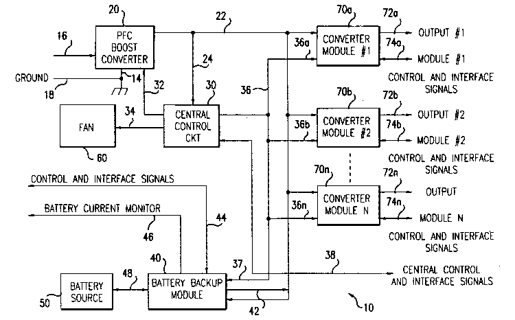
Referring to the Figures, there is shown modular
power supply system 10 for providing highly regulated
voltages to computer and telecommunication systems. As
will be seen in following paragraphs, modular power
supply system 10 includes an input conversion circuit 20
which provides power factor correction, such that system
10 substantially represents a resistive load to the
alternating current voltage source to which system 10 is
connected. The input converter 20 provides power to a
high voltage DC bus 22, from which a plurality of output
modules 70a - 70n draw power and convert such to
respective predetermined output voltages. Further,
system 10 includes a battery backup module 40 for
maintaining the high voltage DC bus power during an
outage of the AC source, allowing the computer or
telecommunications systems coupled to system 10 to be
maintained in operation, or shut down in an orderly
manner.
Referring now to the block diagram of the modular
power supply system 10, shown in FIG. 1, the AC power
21~3171
supplied on line 16 is converted to a high voltage DC
level for distribution to a plurality of output modules
70a - 70n on a DC voltage bus 22. The output modules
down convert the DC voltage supplied on bus 22 to
particular predetermined DC or AC levels for output to
respective loads on the output lines 72a - 72n. This two
stage approach, boost converting the input voltage and
down converting from the boost converted voltage improves
the overall regulation of the system. As will be
described in following paragraphs, the voltage output to
bus 22 is maintained substantially constant for an input
AC RMS voltage on line 16 within the range of 90 - 264
volts. With a substantially constant voltage supplied to
the input of the down converter modules 70a - 70b, those
modules are better able to regulate their respective
outputs, with their input voltage being substantially
invariant. The arrangement further provides for an
efficient means to incorporate a battery backup function,
the battery backup module 40 monitoring the voltage of
bus 22 and maintaining such at a predetermined level
21~3171
without introducing any switching transients or time
delay between loss of the AC input voltage and power
being supplied from the battery source.
Thus, boost converter 20 functions to convert the AC
power supplied on line 16 to a high voltage DC output
supplied to the DC voltage bus 22, in a manner which
makes system 10 appear as a substantially resistive load
to the AC source.
As is conventional with large power supply systems,
the system ground 14 is coupled to an external earth
ground by a line 18. Although each of the modules
coupled to the DC bus 22 include their own discrete
control circuitry, system 10 includes a central control
circuit 30 for coordinating the operations of system 10,
providing alarms to external devices, providing for start
up of the system and emergency shut down thereof.
Central control circuit 30 generates bias voltages and
synchronization signals which are output to each of the
down converter modules 70a - 70n on the output line 36
for respective coupling to each of the modules by the
2143171
lines 36a - 36n. Central control circuit 30 also
provides an output 32 which is coupled to the power
factor corrected boost converter 20 to provide a
synchronization signal and bias voltage thereto. The
generation of the bias voltages which are supplied to
each of the modules define the power source for the
amplifiers and logic circuits therein, and thereby
provide an efficient means for shutting the system down
from a central point in the system, as will be further
i described. Central control circuit 30 monitors the
thermal conditions of system 10 and also provides the
operational voltage to a DC fan 60 by the coupling line
34. Additionally, control circuit 30 monitors the
voltage level of bus 22 by means of the coupling line 24
in order to provide for start up of the system and
properly generate the bias voltages supplied to each of
the modules and the power factor corrected up converter
20.
System 10 may include at least one converter module,
with additional modules added as required to meet the
2143171
11
demands of a particular application. Although such
converter modules are typically down converters, they may
be up converter modules for applications requiring such.
Each of the modules 70a - 70n derive their input power
from the DC voltage bus 22, and are designed to provide a
predetermined regulated output voltage on their
respective output lines 72a - 72n. The down converter
modules are designed to maintain a substantially constant
output voltage, which may be AC or DC, depending upon the
particular application, with a variation of input voltage
within the range of 300 - 420 volts, with the voltage on
bus 22 being maintained at substantially 390 volts by
boost converter 20. Each of the down converter modules
70a - 70n also provides alarm and interface signals to
the particular load to which they are connected, through
a respective control and interface signal bus 74a - 74n.
Such interface signals may include a shut down control
signal transmitted from the load to the down converter
module, to disable the output therefrom responsive to
some external condition.
2143171
12
It is particularly important to the application of
modular power supply system 10 in critical computer and
telecommunications applications that it maintain the
regulated output voltage from each of the respective down
converter modules 70a - 70n during interruptions in the
AC power supplied on line 16, which is accomplished by
means of the battery backup module 40. The battery
backup module is coupled to the bias and synchronization
signal output of central controller circuit 30 by means
of the coupling line 37, and is coupled to the DC voltage
bus 22 for monitoring the magnitude of the voltage
thereon. Battery backup module 40 provides an output 42
coupled to DC voltage bus 22 for supplying a DC voltage
output, responsive to a drop in the bus voltage from the
nominal 390 volts to a level approximating 360 volts.
Thus, if the AC voltage on line 16 is interrupted, the
power factor correcting boost converter 20 will cease to
generate voltage, resulting in its output filter
capacitors discharging. The bus voltage will thereby
begin dropping, and as such reaches 360 volt~, the
2143171
13
battery backup module 40 will generate sufficient power
to maintain the bus voltage at the 360 volt level,
without generating any transience or glitches in the
voltage on bus 22. As the change from 390 volts to 360
volts will not affect the regulated output of the down
converter modules 70a - 70n, the respective output
voltages on outputs 72a - 72n are unaffected by the
transfer from AC power to the battery backup source 50.
The battery backup module 40 is coupled to the battery
l source 50 by a DC bus 48 for carrying battery power to an
up converter of module 40 and carries power to the
battery from a battery charger circuit of the module 40.
Module 40 further supplies battery charger alarm, logic
and battery current monitoring signals to external
systems through the coupling line 46, and receives
control and interface signals from external systems on
the bus 44.
Referring now to FIG. 2, there is ~hown a circuit
diagram for the power factor correcting boost converter
20. AC voltage from the source 12 is supplied by the
21~3171
14
lines 16 to the electromagnetic interference filter 100
which prevents high frequency noise generated by the
inverter circuits of system 10 from being fed back into
the AC lines. The output of EMI filter 100 is supplied
to the AC input terminals 106, 108 of the rectification
circuit 110. The output of rectifier circuit 110 is
coupled to an in-rush current limit circuit 120, which
limits the starting current flowing from rectifier 110
during an initial start up time period. Rectifier
l circuit 110 includes a negative voltage output terminal
114 which is coupled to the system ground 116, and a
positive voltage output terminal which is coupled to one
end of a current limiting resistor 118. After the
initial start up time period has lapsed, a pair of
switching devices 122 and 124 of the in-rush current
limit circuit 120 bypass resistor 118 to permit a maximum
current to pass to the high voltage DC bus 22.
Switching devices 122 and 124 may be silicon
controlled rectifiers (SCRs) each having its anode
coupled to a respective AC input terminal 106, 108 of
21~3171
rectifier 110. The gate voltage supplied on line 123 is
referenced to the line 127, also part of bus 32, and
coupled to the cathodes of the SCRs 122 and 124. A node
121 disposed between the series coupling of current
limiting resistor 118 and diode 126 is coupled to the
positive voltage line 22a of DC voltage bus 22 through
the bypass diode 128. Thus, on initial start up, the
rectified voltage from rectifier output terminal 112 is
coupled to the positive voltage line 22a of DC hiqh
voltage bus 22 by the series circuit comprising resistor
118 and diode 128, which provides current limiting by
virtue of the impedance of resistor 118.
The generation of the gate drive voltage for SCRs
122 and 124 will be described in following paragraphs,
however, subsequent to such being generated and supplied
to the respective gates of SCRs 122 and 124 by line 123,
resistor 118 is effectively removed from the circuit.
When SCRs 122 and 124 are turned on, alternating half
cycles of the AC voltage supplied to the respective
anodes thereof is supplied to the node 125 for coupling
2143171
16
to the positive voltage line 22a through the boost
circuit 129.
The inverter boost circuit 129 include~ a current
transformer 142 having a primary winding 144 through
which an oscillation or pulsating current flo~s
responsive to the repetitive switching on and off of the
switch 148. Current transformer 142 provides feedback of
the current flowing through switch 148. Switch 148 may
be any solid state switching device such as a MOSFET
I switching device, or alternately a plurality of MOSFET
switching devices coupled in parallel. Switch 148 is
turned on and off responsive to a switching control
signal supplied from the DRIVE output terminal of the
pulse width modulator/power factor correction circuit 150
by the coupling line 152. Thus, DC voltage supplied to
node 131 passes through an inductor 130, for coupling to
one end of the primary winding 144 of current transformer
142, and from the opposing end of primary winding 144
through the switching MOSFET 148 to the system ground
116. When the MOSFET 148 is switched from a conductive
2143171
17
to a nonconductive condition, a high voltage is induced
in the inductor 130 to boost the voltage supplied to the
node 131, by flyback voltage inducted in the inductor.
The voltage supplied to node 131 is coupled to the
positive voltage line 22a of the DC high voltage bus 22
through the current monitoring transformer primary
winding 134 and at least one series coupled blocking
diode 138. The reference voltage line 22b of the voltage
bus 22 is coupled to the system ground 116, and a storage
capacitor 140 is coupled across the bus voltage lines 22a
and 22b for providing low frequency filtering and charge
storage. Capacitor 140 may be one or more capacitors
combined to have a value within the range of 1400 - 1500
microfarads.
The voltage on the positive voltage bus line 22a i6
fed back to the voltage feedback input terminal Vy of
pulse width modulator/power factor correction circuit 150
by means of the coupling line 162, the resistor 160 and
the coupling line 164. The pulse width modulator/power
factor correcting circuit 150 controls the switching of
21~3171
18
MOSFET 148 so as to regulate the voltage generated in
inductor 130, and maintain a regulated voltage of 390
volts impressed between the DC voltage bus lines 22a and
22b. The switching of MOSFET 148 is controlled so as to
generate a current in inductor 130 which is reflected at
the input 16 as a current whose phase is maintained in
close relation to the phase of the voltage from the AC
source.
In addition to regulating the voltage of bus 22,
pulse width modulator/power factor correction circuit 150
controls the current supplied to the bus as well as
regulating the voltage, the current feedback information
being supplied by the secondary winding 136 of current
monitoring transformer 132 and secondary winding 146 of
current monitoring transformer 142, which are coupled in
parallel relation. Secondary winding 146 provides
feedback of the current flowing through the switching
device 148. The two secondary winding~ 136 and 146 are
each coupled in series with a respective diode 156 and
154, the cathode of both diodes being coupled
21~317i
19
together to the system ground 116. The opposing end of
each of the windings 136 and 146 are coupled together for
providing an output to the feedback current input
terminal I~ of the pulse width modulator circuit 150,
through the coupling line 158. Resistor 141 and
capacitor 143 are coupled in parallel relation between
the feedback coupling line 158 and ground 116 to provide
filtering thereof. The windings 136 and 146 are phased
such that each provides a signal on alternate half cycles
of the switching signal supplied on line 152, thereby
time division multiplexing the respective current
feedback signals. Thus, the pulse width modulator
circuit 150 may vary the duty cycle of the control signal
which drives MOSFET 148 in order to control the current
which flows through the switching device as well as the
current which is supplied to bus 22, and vary the duty
cycle of the control signal in order to regulate the
voltage induced in inductor 130.
The pulse width modulator/power factor correction
circuit 150, in order to maintain an input current which
2143~7~
is in phase with the AC input voltage, monitors the input
signals supplied to the system. The input signals are
represented by the rectified voltage supplied to node 125
and a current drawn therefrom. A representation of the
AC voltage is supplied to the AC input voltage terminal
VAc through a voltage divider defined by resistors 153 and
155, the center tap therebetween b~ing coup}ed to the VAc
terminal by the coupling line 157. The series
combination of resistors 153 and 155 are coupled between
the node 125 and the system ground 116. A representative
current is supplied to the AC current input terminal IAC
of pulse width modulator 150 from node 125 through the
resistor 151 and coupling line 159. Pulse width
modulator circuit 150 utilizes the waveform of the
current passing through resistor 151 as a reference for
generating a full wave sinusoidal current in inductor 130
to derive substantially unity power factor at the input.
Two of the control signals provided from the central
control circuit 30 are the bias supply voltage, supplied
to the voltage supply terminal Vcc of pulse width
21~3171
21
modulator 150 by means of the coupling line 196, an a
synchronization signal supplied by line 198 and coupled
to the SYNC input terminal of circuit 150. Pulse width
modulator circuit 150 also includes an enable/inhibit
input terminal INH for inhibiting the output from the
drive terminal responsive to a signal supplied to the INH
input. Several logic functions are coupled to the INH
input terminal for inhibiting generation of the boost
voltage responsive to particular predetermined
l conditions.
One such condition for inhibiting generation of the
boost voltage is an input undervoltage condition. After
the system has completed the start up cycle, if the input
voltage subsequently.drops below 80 volts, the boost
voltage generation is shut down. If the battery backup
module is not available when the input voltage drops
below 80 volts, then the whole system is shut down. The
positive output voltage terminal 112 of rectifier 110 is
monitored to provide a representation of the input AC
voltage. Thus, a current limiting resistor 184 i~
21g3171
coupled to terminal 112 to provide the input voltage
representation to the comparator 186 via the coupling
line 195. Comparator 186 compares the voltage supplied
on coupling line 195 with a first reference voltage V~E~1.
The output of comparator 186 is coupled to an inverter
190 by the coupling line 188, the output 192 of inverter
190 is coupled to the inhibit input terminal pulse width
modulator circuit 150 by coupling line 172. The output
of comparator 186 is also coupled to an input of the
l logic circuit 180 by the coupling line 174. Logic
circuit 180 provides a system shut down output on line
175 responsive to the signal on line 174 indicating that
the input voltage has dropped below 80 volts and an input
signal supplied from an interlock switch 183 on line 182
indicating that the battery backup module is either
present or not.
The bus voltage supplied on line 22A, supplied
through resistor 160 is also coupled to the comparator
168, by the coupling line 166. Comparator 168 compares
the voltage on the bus with a second reference volta~e
2143171
V~E~2, supplied to the comparator 168 by the coupling line
178. The output 170 of comparator 168 is coupled to the
inhibit input terminal INH by the coupling line 172. The
second reference voltage VIE~2 is selected such that the
boost voltage is limited to a maximum value of
approximately 450 volts, which will protect the battery
backup module and the output converter modules from an
overvoltage condition.
Referring now to FIG. 3, there is shown, the battery
backup module 40 which comprises two major components, a
charger 200 and a battery up converter 250. The charger
circuit 200 is basically a down converting inverter
circuit for converting the 390 volts DC supplied on bus
22 to a 56 volt DC level for charging the backup
battery 50. This inverter circuit includes a controlled
leakage inductance transformer 202 having a primary
winding 204 coupled in series with a switching device 212
across the voltage bus 22. The leakage inductance of
this and other transformers of system 10 are controlled
by virtue of their construction using flat conductors
2143171
2~
formed on a flexible insulator which is wound on a
bobbin. ~witching device 212 may be a single MOSFET
device, or a parallel arrangement of such devices
controlled by a pulse width modulator circuit (PWM) 216.
For simplification, the feedback connections to pulse
width modulator 216 have not been shown, as such may be
derived in a similar manner to that which has been
described for the power factor correction of converter
circuit 20, and such feedback connections for pulse width
l modulators are well known in the art. PWM 216 has an
output drive signal supplied to the gate of the MOSFET
switching device 212 through the coupling line 216. The
high frequency switching of current through the primary
winding 204 induces a voltage in the secondary winding
206 which is rectified by diode 208 and filtered by
capacitor 210, to provide a voltage on the battery supply
bus 48 for charging battery 50. The negative supply line
48b of bus 48 is coupled to the battery system ground
116' to provide a reference for the positive battery
voltage supplied on line 48a. The battery voltage is
2143171
supplied to the battery up converter 250 through the
coupling line 222, which is monitored by the interface
circuit 232.
The battery voltage is coupled to interface circuit
232 by the input coupling line 234, wherein the battery
voltage is compared with a third reference voltage V~gg3
supplied to the circuit on line 228. The output of
interface circuit 232, indicating an overvoltage
condition, as when the battery is electrically removed,
i is supplied on coupling line 46, which provides logic
level alarm signals to an external system, such as the
computer or telecommunications system which is being
powered by system 10. The presence of the battery is
also monitored by the comparator 240, which receives the
battery voltage through the input coupling line 238,
providing an output on line 242 to the optical coupler
218 through the coupling line 246, responsive to the
voltage on line 238 being less than the third reference
voltage which is supplied to the comparator 240.
Other connections, not shown, to interface circuit
232 may provide such information as charging current,
2143171
26
battery load current, a low battery voltage indication, a
battery open indication and various temperature
measurements. An output from the battery up converter,
provided on line 296, is coupled to the node 244,
disposed between the output of comparator 240 and the
input of optical coupler 218, for inhibiting the
operation of the charger when the up converter 250 is
enabled. Thus, the pulse width modulator is inhibited
responsive to a signal on line 248 from the optical
coupler which in turn is generated responsive to either
an output from comparator 240 indicating the battery
voltage is less than the third reference voltage, or an
output from the interface logic circuit 290 of the up
converter 250 indicating that the voltage bus 22 is being
supplied power from the up converter 250. The pulse
width modulator 216 is supplied with a synchronization
signal on line 220, and provided with a DC operating
voltage by the line 298.
The battery up converter 250 includes an up
converter circuit utilizing a controlled leakage
2143171
27
inductance transformer 251 for generating a 360 volt DC
output from the 48 volt battery source. The battery
voltage is supplied from the positive bus line 48a to the
center tap 254 of inverter transformer primary winding
252 by the coupling line 222. Each of the opposing ends
of the primary winding 252 of transformer 251 are
respectively coupled to a switching device 278, 282 for
alternately drawing current through a respective half of
winding 252. By this arrangement, one end of winding 252
i is coupled to the drain 284 of the MOSFET switching
device 282, with the source 286 of device 282 being
coupled to the battery system ground 116', to thereby
complete a current path from the positive lead of battery
50, through the center tap of winding 252 through one
half of the primary winding 252 to the battery ground
reference 116'. Similarly, the opposing end of winding
252 is coupled to the drain 279 of the MOSFET switch 278,
its source 280 being coupled to the battery system ground
116'.
A pulse width modulator circuit 70 provides
respective drive outputs 274, 276 which are coupled to
214~171
28
the respective gates of MOSPETs 278, 282, switching each
on in alternate half cycles. Responsive to the
alternating current driven through the respective
portions of primary winding 252, a voltage is induced in
the secondary winding 256 of controlled leakage
inductance transformer 251 which is coupled to the
rectifier and filter circuit 260. Here again, the
feedback signals for maintaining regulation of the
induced voltage is not shown for simplicity.
When the high voltage DC bus 22 is above a
predetermined level, the operation of pulse width
modulator 270 is inhibited, the output drive signals
being inhibited while the remainder of the circuit is
operational, such as the high frequency oscillator and
feedback monitoring circuits, such that the drive signals
can be properly supplied to the MOSFET switches when the
inhibit signal is removed. The voltage on the positive
bus line 22a is coupled to the up converter output line
42a and from there to the logic circuit 264 by the
coupling line 262. Control circuit 264 compares the
214~17 L
29
voltage on the bus line 22a with a reference voltage so
as to provide an output error signal on line 266
responsive to the voltage on bus line 22a for regulating
the bus at 360 volts, and thereby inhibit voltage
generation when the bus voltage is greater than 360
volts.
The output from control circuit 264 on line 266 is
coupled to an optical coupler circuit 268, for providing
isolation. The output of optical coupler circuit 268 is
supplied to the pulse width modulator 270 by coupling
line 272. Thus, when the voltage is properly generated
by the power factor corrected boost converter circuit 20,
the voltage on bus line 22a will be approximately 390
volts, which will in turn result in an output signal from
control circuit 264 which inhibits the operation of pulse
width modulator 270. If however the AC voltage input to
the power factor corrected up converter 20 is lost for
any reason, capacitor 140, shown in FIG. 2, will begin to
discharge, and as the discharge voltage drops to 360
volts, control circuit 264 will generate an error signal
21g3171
which will allow pulse width modulator 270 to control the
MOSFET switches 278 and 282. Responsive to the operation
of the MOSFET switches, the secondary winding 256 will
provide an induced voltage to the rectifier filter
circuit 260, for supplying the DC voltage bus 22 with a
360 volt voltage, and thereby maintain power to the
various other modules 70a - 70n coupled to the bus 22.
Particular operating parameters of the battery up
converter 250 are supplied to the interface logic circuit
1 290 by the coupling line 292 for output to external
systems on the interface bus 44. Further, an output from
interface circuit 290 is provided to the charger through
the coupling line 296 to inhibit the charger's operation
during operation of the up converter. A synchronization
signal from the central control circuit 30 is provided to
the pulse width modulator 270 by means of the coùpling
line 288. Further, the DC voltage for powering the logic
circuits, the bias voltage, is supplied on line 298 to
the interface logic circuit 290, pulse width modulator
270 and control circuit 264 of the up converter 250, as
2143171
31
well as to the pulse width modulator 216 and interface
circuit 232 of the charger 200.
Periodically, it may be desirable to test the
battery backup module 40 to insure that such is
operational and performs to specification. However,
where the modular power supply system 10 is coupled to a
live load, one which must be maintained operational, it
would be imprudent to simply remove the AC power source
as the means of testing the battery backup function. It
is therefore desirable to provide a means for testing the
operation of the battery up converter 250 without the
danger of losing the ability to maintain the voltage of
bus 22. Such a battery backup test function has been
incorporated into the system 10. An external signal
supplied to the battery test input terminal is coupled to
the control circuit 264 by the coupling line 299. This
logic signal is coupled to the pulse width modulator 270
through an optical channel of the optical coupler circuit
268, such coupling being represented by the coupling line
272. The function of this signal is to shift the voltage
2143171
32
regulating operating point of pulse width modulator 270
from 360 volts to 415 volts.
Responsive to this test signal, the pulse width
modulator 270 is enabled with the bus voltage at the 390
volt level, and is raised to 415 volts by the up
converter circuit 250. The internal error amplifier of
the PWM 150 of the power factor correction boost
converter circuit 20 senses the bus voltage is above 390
volts, and thus shuts down the output drive signal to the
i MOSFET 148, while maintaining its other circuit functions
in an operational state. Obviously, if there is a
problem in the battery backup module 40 which does not
permit the generation of the DC output voltage on the
output lines 42, the DC voltage bus 22 will be maintained
at the 390 volt level, the load will remain undisturbed,
and an alarm signal will be output from interface logic
circuit 290.
If the battery backup module 40 operates properly
when in the battery test mode, the voltage on the bus
will be raised to the 415 volt level, the power factor
3 2143171
correction up converter circuit 20 will be shifted to a
standby mode and the regulation of the output modules 70a
- 70n will be unaffected by the small increase in bus
voltage. Subsequent to removal of the battery test
signal, the operation of pulse width modulator 270 will
be inhibited, since its operating point will be returned
to 360 volts and the bus voltage will be above 360 volts.
The voltage on the DC voltage bus 22 will bleed off, and
such will be sensed by the error amplifier of the PWM
150, which will reactivate the output drive signal of the
pulse width modulator 150 once the bus drops to
approximately 390 volts.
Referring now to FIG. 4, there is shown the central
control circuit 30 which supplies synchronization and
bias voltages to the various modules of the system 10.
When system 10 is initially energized, the voltage
supplied to the DC bus 22 begins to rise from a zero
value, the voltage initially being supplied through the
in-rush current limiting resistor 118 and bypass diode
128. During this initial time period the pulse width
~14~171
34
modulator 150 of the power factor correction boost
converter circuit is not operational, as there is not yet
sufficient voltage on line 196 to properly power pulse
width modulator 150. The DC voltage initially supplied
to the voltage bus line 22a is coupled to a voltage
source 370, formed by a constant current source supplying
a capacitor, through the coupling line 376 for providing
an operating voltage (Vcc) to pulse width modulator 340.
The voltage on bus line 22a is also supplied to one end
of the primary winding 302 of the transformer 300, which
may also be a controlled leakage inductance transformer.
The opposing end of primary winding 302 is coupled in
series relation with the switching device 344, which may
be one or more MOSFET switching devices having a drain
connection 346 coupled to primary winding 302 and a
source connection 348 coupled to the system ground 116.
Thus, as the voltage on the bus line 22a begins to rise,
the pulse width modulator 340 operates to switch current
through the primary winding 302. Responsive to the
switching current in primary winding 302, the
2143171
multiplicity of secondary windings of transformer 300
generate induced voltages therein. As the voltage
increases on bus line 22a, the respective voltages
generated in the secondary windings of transformer 300
also increase.
The voltage induced in secondary winding 304 is
rectified by diode 380 and filtered by capacitor 382.
The anode of diode 380 is coupled to one end of winding
304 through the current limiting resistor 378, the
I opposing end of winding 304 being coupled to the
reference voltage line 127. The rectified voltage from
diode 380 is coupled to the gate drive line 123 which is
in turn coupled to the gates of SCRs 122 and 124, shown
in FIG. 2 and the reference line 127 is coupled to the
cathodes of SCRs 122 and 124 to provide a reference for
the gate voltage. Thus, when the voltage generated on
line 123 is sufficient to turn on SCRs 122 and 124, the
in-rush current limiting resistor 118 is thereby
bypassed.
The pulse width modulator circuit 150, shown in FIG.
2, receives its power from a bootstrap voltage generating
21~3171
36
circuit 368. Bootstrap voltage generating circuit 368
generates sufficient voltage for operating the pulse
width modulator 150 during the initial start up phase,
then subsequently provides a change in transformation
ratio to prevent the supply voltage from exceeding
predetermined limits. By providing such a transformation
ratio change, limiting the voltage generated by the
bootstrap voltage generating circuit, allows the use of
Shottkey type rectifying diodes, which are more
efficient. When the output of the bootstrap voltage
generating circuit 368 is sufficient to power the pulse
width modulators 150 and 340, an output signal supplied
on line 372 shuts down the voltage source circuit 370,
thereby allowing the bootstrap voltage generator circuit
to supply power to the pulse width modulator 340 through
the coupling line 374.
The output drive signal of pulse width modulator
340, supplied to the MOSFET 34~ on line 342 is coupled to
the power factor correction and charger sync circuit 356
through the coupling line 354. The synchronization
2143171
37
circuit 356 utilizes the oscillation signal from the
pulse width modulator to provide synchronization signals
to pulse width modulator 150 through the coupling line
198 and to pulse width modulator 216 of charger circuit
200 through the coupling line 220. The secondary winding
306 is coupled to a voltage sense circuit 336, which
provides an output to the bootstrap voltaqe generator
circuit through the coupling line 338 when the induced
voltage of winding 306 exceeds a predetermined value.
l The signal from voltage sense circuit 336 is
utilized to change the transformation ratio which
provides the input thereto. The voltage generated by
bootstrap voltage generator circuit 368 is derived from
the output of the secondary winding 308, which is the
combination of voltages induced in the tapped winding
portions 310 and 312. Responsive to the signal output
from voltage sense circuit 336, the winding 310 is
preferably opened, thereby reducing the magnitude of the
input voltage to the voltage generating circuit 368.
Transformer 300 includes a plurality of secondary
windings 314a - 314n for providing bias voltage to the
21~3171
various modules of system 10. Each of the windings 314a
- 314n is coupled to a respective bias rectifier and
filter circuit 318a - 318n for supplying bias voltage and
synchronization signals to the respective modules. The
bias rectification and filter circuits may include a pair
of diodes 322 and 324, each having an anode thereof
coupled to an opposing end of the secondary winding 314a.
the cathodes of each diode are respectively coupled to
the sync signal line 402 for coupling to a respective
down converter module circuit 70. The common cathode
connection of diodes 322 and 324 is also coupled to one
end of a choke 326, the opposing end of choke 326 being
coupled in series relation with the parallel RC circuit
formed by capacitor 326 and resistor 327, and the DC
output line 404 which supplies the power supply voltage,
with respect to a module ground 116'', to the logic and
pulse width modulator circuits of the respective down
converter module, to which it is coupled.
Such a rectification and filter circuit is provided
for each of the down converter modules 70a - 70n of
2143171
39
system 10. One of the rectification and filter circuits
318n supplies synchronization signals, output on line
288, to the pulse width modulator 270 of the battery up
converter 250, shown in FIG. 3. The DC voltage supplied
on line 298 provides the operating voltage for the pulse
width modulators and logic circuits of the battery backup
module 40. An additional secondary winding 316 is
coupled to a logic power supply circuit 320 for powering
the DC cooling fan 60 of system 10 and the logic circuits
l of the central control circuit 30. A DC output voltage
supplied on line 34 powers the fan 60, and on line 358
for powering the control and interface logic circuit 330,
and the logic circuit 360. Line 196, in addition to
supplying PWM 150 also provides power for the comparators
168, 186 and 190 of boost converter 20, delaying their
energization and that of PWM 150 relative to pulse width
modulator 340, such that the low voltage inhibit function
does not interfere with initial start up of system 10.
The control and interface logic circuit 330 monitors the
operation of the DC fan, through the fan fail monitoring
2143171
line 332, receives a status from the output modules on
line 36, and outputs alarm and status signals on the
interface bus 38.
The generation of the bias voltages for powering the
logic circuits of all of the modules in system 10
provides a unique and efficient means for providing a
shut down of the entire system. When conditions indicate
that the whole system should be shut down, such as when
the input voltage drops below 80 volts and the battery
backup module is not present, logic circuit 180, shown in
FIG. 2, outputs a shut down signal on line 175. That
signal is coupled to the logic circuit 360 of the central
control circuit 30. Logic circuit 360 provides an output
signal of appropriate polarity to the optical coupler 364
by means of the output coupling line 362. Optical
coupler 364 provides an optically isolated signal output
on line 366 for inhibiting the output of pulse width
modulator 340. Thus, the switching device 344 is
maintained in an off state to thereby cease the induction
of voltage in the plurality of secondary windings of
41 214317 ~
transformer 300. Hence, the DC voltages that were
supplied to the logic circuits and pulse width modulators
of each of the ~utput modules, the battery backup module
and the power factor corrected boost converter are
substantially simultaneously cut off, quickly shutting
down the entire system from a central point. As shown in
the representative bias rectifier and filter circuit
318a, each of the bias supplies is provided with a bleed
resistor 327, such that the bias voltage is quickly
brought down when the induced voltage supplying the
rectifier circuit is cut off.
Referring now to FIG. 5, there is shown a typical
output module 70a for converting the high voltage
supplied on the DC bus 22 to a predetermined output
voltage on the output lines 72a for use by a
predetermined load. The DC voltage bus 22 is coupled to
a high frequency inverter 400 whose output is coupled to
a rectifier and filter circuit 434 to supply the required
DC voltage on the output lines 72a. Inverter 400 is a
bridge type switching circuit, sometimes referred to as
2143171
42
an H-switch circuit, wherein the output is taken from the
coupling between the central portion of each leg thereof.
Each leg comprises a pair of switching devices coupled in
series relation which are operated alternately. Each of
the respective four MOSFETs 406, 408, 410 and 412 have
their respective gates coupled to the output drive
terminals l~ 2~ 3 and O~ of the phase shift pulse width
modulator 436 by the respective coupling lines 438, 440,
444 and 442.
Phase shift pulse width modulator 436 controls the
operation of each of the four MOSFET switching devices
such that the MOSFETs 406 and 412 are turned on during
one portion of an AC cycle and MOSFETs 408 and 410 are
operated during an alternate half cycle, to provide bi-
directional current flow through the primary winding 426
of the controlled leakage inductance transformer 424. In
order to provide the minimum stress on the circuit
components and minimize the generation of harmonic
signals, the switching of current through primary winding
426 is best accomplished when the voltage across each
43 2 1 4 3 17i
MOSFET is 0 volts. To accomplish this 0 voltage
switching, the energy which is stored in primary winding
426 and the leakage inductance 422 of transformer 424
must induce a voltage equal the bus voltage. It is for
this reason that it is important that the leakage
inductance of transformer 424 be predictable and
consistent from one transformer 424 to another, and since
the leakage inductance is additive, it is equally
important that its value be similarly known and
controlled.
Each of the MOSFET switching devices has an
intrinsic capacitance 414, 416, 418 and 420 between the
respective source and drain terminals thereof. This
intrinsic capacitance is a known value which is very
consistent from one device to another. The capacitance
value for each of the devices 406, 408, 410 and 412 is a
relatively low value, in the picofarad range. Therefore,
it is desirable to have a suitable inductance coupled
therewith to form a resonant circuit, such that the
stored energy can be efficiently transferred. Since the
21~317~
leakage inductance 422 effectively appears as an
inductance value which is in series with the mutual
inductance reflected in the primary winding 426, such is
shown as a separate element coupled in series with the
primary winding 426 between the output nodes 407 and 411.
The alternation of current through primary winding
426 induces a voltage in secondary winding 428, the
opposing ends of which are coupled to the rectifier and
filter circuit 434 through the coupling lines 432 and
430. Obviously, if an AC voltage is desired for supply
to a particular load, the rectifier filter circuit 434
may be eliminated and the output from the secondary
winding 428 provided thereto. Feedback from the output
voltage line 72a is supplied to the "Sens" input of pulse
width modulator 436 by the coupling line 452, feedback
logic circuit 454, and coupling line 448, allowing the
phase shift pulse width modulator 436 to control the
switching of the respective MOSFETs 406, 408, 410 and 412
to maintain the output voltage or current at a
predetermined level. Here again, conventional
2143171
connections for feedforward, and current feedback have
not been shown for purposes of clarity.
Thus, the feedback line 452 may represent voltage or
current feedback, for discussion purposes. The feedback
signal from line 452 is applied to the output line 448 of
feedback logic circuit 454, unmodified, if no control
signal is input on line 456 from control and interface
logic circuit 446. The output module 70a further
includes a control and interface logic circuit 446, for
1 providing the inhibit signal to the phase shift pulse
width modulator 436, by means of coupling line 450, as
well as providing an interface for alarm and other
signals which are exchanged between the module 70a and
the particular load to which it supplies power. Control
and interface logic 446 also provides a status output on
line 36 to the control and interface logic circuit 330
(FIG. 4), indicating whether the output module is
operating properly or not. A synchronization signal is
supplied on line 402 to the SYNC input of pulse width
modulator 436 and the bias supply voltage form the
21i3171
46
circuit 318a is supplied on line 404 to the Vcc input of
pulse width modulator 436 and the voltage supply input of
the control and interface logic 446, which permits the
system to be shut down, as was previously described.
Multiple output converter modules 70 may be coupled
in parallel to a load with the load current being equally
divided among the paralleled modules. When this option
is utilized, a control signal is input on the respective
interface bus 74. Thus, if module 70a is being
l paralleled with module 70b, or a module 70a of another
power supply system, then the power sharing control
signals will be respectively on the buses 74a and 74b.
This control signal, as shown in FIG. 5, is input to the
control and interfacç logic circuit 446 of each module.
The control and interface logic circuit 446 outputs a
control signal to the feedback logic circuit 454. In
response to the input from signal line 456, feedback
logic circuit 454 modifies the feedback signal provided
from feedback line 452 to generate a signal on line 448
which maintains a load current value substantially equal
to that of the other paralleled module 70b.
- -
2143171
Although this invention has been described in
connection with specific forms and embodiments thereof,
it will be appreciated that various modifications other
than those discussed above may be resorted to without
departing from the spirit or scope of the invention. For
example, equivalent elements may be substituted for those
specifically shown and described, certain features may be
used independently of other features, and in certain
cases, particular locations of elements may be reversed
i or interposed, all without departing from the spirit or
scope of the invention as defined in the appended Claims.