Note: Descriptions are shown in the official language in which they were submitted.
W094/06054 21 4 3 8 4 6 PCT/GB93/01897
-- 1 --
NON-T,TN~R S~MTCONDUCTOR OP~ICAT D~VIC~
The present inventlon relates to a non-linear
semiconcuctor optical device. Such devices find application
in optical communications systems, for instance as switches.
Embodiments of the present invention can show a
relatively large and fast optical non-linearity and thus lend
themselves to exploitation for instance in high speed or high
data rate optical communication systems.
Communications llnks which can carry high data rates
10 are advantageous because they can transmit increased levels
of information and/or can provide links via a single physical
connection whi~h services higher numbers of customers. For
instance, time division multiplexed signals on a
communications link can provide a higher number of time
15 slots, and potentially therefore service a higher number of
customers, where the link itself carries a higher data rate.
Alternatively, ultra high bit rate links may enable customers
to be offered large bandwidth services, and/or give
telecommunications companies greater flexibility in managing
20 their networks.
In order to access the data on a communications link,
it is necessary to download the information on the link to a
receiver. To do this, switching devices may be used, the
speed of switching of the device being commensurate with the
25 capability of the link for carrying high speed traffic. In
optical communications, it is envisaged that data rates may
be achieved as high as 100Gbit/s or more, in the foreseeable
future. This might be carried for instance in ten time
slots, providing ten channels at 10Gbit/s.
Data rates of 100Gbit/s or higher will require all-
optical switching elements since electronic components
operatlng at such speeds are not available. Embodiments of
~ the present invention can provide an important part of
achieving ultra high bit rate links, providing a switching
35 device potentially capable of demultiplexing for instance a
10Gbit~s blt s.ream from a 100Gbit/s optical time divisior
W094t06054 PCT/GB93/01897 _
2 1 43 8 46 - 2 -
multiplexed (OTDM) signal. An optical pump synchronised to
the data stream might be used to switch out every tenth blt.
Applications of a large, fast optical non-linearity
such as that provlded by embodiments of the present invention
go beyond just high data rate optical communication systems.
In particular, there will be applications in all-optical
processing and logic systems. A reference in this respect is
a review paper: "Third Order Non-Linear Integrated Optics"
by G I Stegeman et al., Journal of Lightwave Technology, vol
i0 6 953-970 June 1988. This describes a range of devices and
applications, many of which could be exploited using
- embodiments of the present invention.
A further desirable characteristic in an optical
switching device is the combinatlon of high speed of
15 operation with moderate optical power requirements for
~switching, preferably the optical switching power being
generated from a conventional source for optical
transmission.
Recently, a large above-bandgap ultrafast optical non-
20 linearity has been observed in active waveguides driven atthe material transparency current. The above-bandgap non-
linearity is reported in two papers, as follows:
"Observations of Ultrafast Non-Linear Refraction in an
InGaAsP Optical Amplifier", published in Applied Physics
25 Letters volume 58 pages 1119-1121 (1991) by R S Grant and W
Sibbett, and "Ultrafast Refractive Index Dynamics in AlGaAs
Diode Laser Amplifiers~, published in Applied Physics Letters
volume 59 page 635 (1991) by C T Hultgren and E P Ippen.
In an active waveguide as discussed herein, there is
30 an optically confined active region of material which can be
supplied in use with a drive current to produce gain by
stimulated emission in optical radiation propagating through
the active region. In the absence of electrical injection by
means of the drive current, this active region leads to
35 interband absor?tion of light for wavelengths shorter than
the bandgap equivalent wavelength. The st~ucture is designed
such that cu_rent injection produces electron/ho~e
2l438~6
W094/06054 PCT/GB93/01897
.", ,_
-- 3
populations in the active region, countering the interband or
stimulated absorption with the stimulated emission to a
degree determined at least in part by the drive current, over
a range of wavelengths corresponding to the gain bandwidth,
between the bandgap equivalent wavelength and some shorter
wavelength. For a given wavelength there is then a "material
transparency current" being the level of current injection at
which stimulated emission and stimulated absorption are
balanced and there is no net change in the carrier
'~ ?opulat_ons induced by the presence of the input optical
pump. It should be noted that stimulated absorption does not
include absorption by processes other than interband
transitions, eg. it does not include defect related losses,
free carrier absorption or scattered light. The material
i5 transparency current is a function of wavelength; while a
transparency current can be found for any wavelength in the
gain bandwidth, for a given device, the value of this current
will depend on the particular wavelength considered. In
practice the short wavelength limit will be determined by the
20 maximum current that can be applied to a particular device,
since higher currents are required to achieve material
transparency at shorter wavelengths.
The term "above-bandgap" is used herein to indicate a
system in which the photon energy of optical radiation used
2~ to trigger the non-linearity is greater than the bandgap
energy of an active region in the device through which the
radiation propagates.
The non-linearity is potentially very attractive for
all-optical switching and processing devices operating at bit
30 rates approaching the Tbit/s range. These devices could work
at switching powers considerably lower than those required by
devices using known alternative ultrafast effects such as the
below bandgap optical Stark effect.
~ The origin of the new, above-bandgap non-linearity is
3 not yet clear. Dynamic carrier effects may contribute, as
may a resonantly enhanced optical Stark effect, not normally
observable in passive waveguides because cf high interband
21438~6
absorption. In the case of active waveguides at
transparency, this optical loss is balanced by gain from the
electrical pumping.
An object of the present lnvention ls to provide a
5 non-linear semiconductor optical device, such as a switch,
- which can offer the combination of a high speed of operation
with moderate optical power requirements.
According to a first aspect of the present invention,
there is provided a non-linear, active, optical semiconductor
10 device for use in data operations in optical communications
systems, the device comprising
i) an active regio~ adapted to receive an optical
signal;
ii) optical pump input means for inputting an optical
pump to said active region, said optical pump
comprising a wavelength shorter than a bandgap
equivalent wavelength of sald active region; and
iii) optical gain determining means for setting said
active region at, or substantially at,
transparency with respect to the optical pump,
such that stimulated emission and stimulated
absoprtion are substantially balanced at the
wavelength of the optical pump radiation,
the arrangement being such that, in use, the optical pump
25 affects the refractive index of said active region in a non-
linear fashion such that transmission of the optical signal
in the device can be controlled.
It has been found, in connection with the present
invention, that there appears to be a significant enhancement
30 of the non-linear effect in quantum well devices rather than
bulk material devices. (That is, as will be understood by a
person skilled in this art, where the active region of a
devlce has a quantum well structure.) A relatively large
non-linear figure of merit has been demonstrated, indicating
35 considerable promise for practical ultrafast switching
systems. In particular, phase shifts of 5~/2 radians in a
lmm long device at 820mW peak optical power have been
AMEN~ED SHEE~
~ 21~38~6
_ - 5
observed in non-optimised devices, which phase shifts were
effectlvely instantaneous on a 20ps time scale.
Where the active region comprises a quantum well
rather than bulk structure, there will be a significant
5 enhancement of the non-linear effect, allowing use of lower
- pump powers for instance. Furthermore it has been found that
if the quantum well material is "strained", for example by
incorporating a lattice mis-match between successive material
layers, the non-linear effect is further enhanced.
The active region may be part of a waveguide
arrangement. The waveguide arrangement may then comprise a
ridge or buried heterostructure waveguide and comprise
semiconductor materials suitable for integration with other
devices in a semiconductor based optical communications
15 system, such as the indium phosphide based materials.
According to a second aspect of the present invention,
there is provided a method of operating an active optical
semiconductor device, the method comprising the steps of:-
1) inputting an optical signal to the active region
of the device;
2) inputting an optical pump, at a wavelength
shorter than the bandgap equivalent wavelength of
the active region, to the active region;
3) adjusting the optical gain of the active region
such that stimulated emission and stimulated
absorption, at the wavelength of the optical
pump, are substantially equal; and
4) controlling the transmission of the optical
signal through the device by utilising the
optical pump to affect the refractive index of
the active region of the device.
Advantageously, the optical signal may be chosen to
have a wavelength for which the material is not at
transparency, ie. the pump and signal wavelengths may be
35 distinct. This allows a device to be operated in a regime
where the signal experiences gain, for example at wavelengths
longer than the pump. Signal wavelengths in the bandgap can
AMENDED SHEEr
21438~6
also be employed. The selection of an optimum signal
wavelength will depend on a balance between the insertion
loss of a particular device and the size of the available
non-linearlty under cross phase modulation conditions. This
5 will depend on the detuning between the pump and signal
wavelengths. Additionally, any dependence on the
relationship between the pump wavelength and the bandgap
equivalent wavelength should be taken into account.
Preferably a region of operation is thus chosen with a large
10 non-linearity where the signal wavelength experiences gain or
at least low loss.
- It will clearly be neeessary in any embodiment of the
present invention that the optical pump has a wavelength for
which a transparency current can be set. This will lie to
15 the short wavelength side of a (or the) bandgap equivalent
wavelength for the active region, for instance within a few
tens of nm of said bandgap equivalent wavelength.
Embodiments of the invention will now be described in
more detail, by way of example only, with reference to the
20 accompanying figures, in which;
Figure 1 shows a bLock diagram of an experimental
arrangement for demonstrating use of a switching device
according to an embodiment of the present invention;
Figure 2 shows spectra for pulses passing through
25 active buried heterostructure waveguide devices according to
embodiments of the present invention, in TE polarisation;
Figures 3a and 3b-show a plan view and cross section
respectively of a directional coupler device structure using
the non-linear effect demonstrated in the experimental
30 arrangement of Figures 1 and 2;
Figure 4 shows a demultiplexer incorporating a
directional coupler as shown in Figure 3;
Figure 5 shows an arrangement for demultiplexing two
separate channels from a multi-channel, high bit rate, data
35 stream, based on cascaded directional couplers;
AMENDE~ SH~L,
2143846
-
- 6A -
Figure 6 shows two configurations of a wavelength
converter incorporating a directional coupler as shown in
Figure 3; and
5Figure 7 shows a non-linear loop mirror incorporating
a laser amplifier set at transparency according to the
- present invention.
Referring to Figure 1, an experimental arrangement for
demonstrating non-linear behaviour of an active waveguide 3
AMENDED SHEET
W094/06054 21 4 3 % ~ 6 PCT/GB93/01897
_ - 7
comprises a pulse source l, coupled via a half wave plate 4
and an input objective 2 to the active waveguide 3 whose
characteristics are being demonstrated. The output of the
waveguide 3 is collected by an output objective 6 and
5 spatially filtered by means of a small aperture 5 before
detection at a detector 7.
It should be noted that the function of the half wave
plate 4 can be provided in other ways and it might for
lnstance be regarde~ as part of the source l.
Non-linear behaviour in the waveguide 3 can be
characterised by observing self phase modulation (SPM) of a
short, high power optical pulse on passing through the
waveguide 3 under conditions of carrier injection. The
pulses used are of 20 to 30ps length, provided by a pulse
15 source l comprising a synchronously mode-locked KCl: Tl~ (l)
colour-centre laser operating at 82MHz, configured to give
stable, transform limited pulses, monitored using an
autocorrelator. The objectives 2, 6 for coupling light into
and out of the active waveguide 3, comprise microscope
20 objectives and the half wave plate 4 controls the launched
polarisation of the input pulses. The aperture 5 is
dimensioned to pass only light in the guided mode in the
waveguide 3 for detection at the detector 7.
The power of the light in the guided mode can be
25 assessed by measuring the power collected behind the aperture
5 and relating this back to power in the waveguide 3 using a
calibration of the aperture 5 from measurements of
spontaneous emission from the waveguide 3. This calibration
is consistent with estimates of the out-coupling efficiency
30 of the microscope objective 6 used.
The optical wavelength of the colour-centre laser used
as the pulse source l (tunable in the l.5~m range) was set to
lie within the gain spectrum of the waveguide 3. SPM
behaviour was seen to be similar across this range, with
35 appropriate setting of the transparency current. A single
device should, therefore, be able to operate at any point
W094/06054 2 ~ 43 ~ ~6 _ 8 - PCT/GB93/01897
across a broad wavelength range (tens of nm) with an
appropriate current bias.
A scanning Fabry-Perot interferometer was used to
monitor the spectrum of the transmitted light from the
5 waveguide 3 and an infra-red vidicon used to observe the near
field patterns.
Measurements were perfor~ed at the material
transparency current. This can be identified by monitoring
the voltage supplied to the waveguide 3 by a constant current
10 source (not shown) in the presence of a modulated optical
signal, a~ dlsclosed in the publication "Electrical
Diagnostics of the Amplifier Operation and a Feasibility of
Signal Registration on the Basis of the Voltage Saturation
Effect in Junction Laser Diodes~ published IEEE Journal of
15 Quantum Electronics volume QE19 pages 1080-1083 (1983), by Vu
-Van Lu'c, Eliseev, P G, Manko, M A and Mikaelian G T. The
modulated optical signal could alternatively be replaced by
pump radiation. Away from transparency, a voltage modulation
is observed, either in phase or in anti-phase with the
20 launched optical modulation. At transparency the amplitude
of modulation goes through zero as the incident light does
not then affect the carrier population in the waveguide.
This is a convenient way of setting the material transparency
current and may provide the basis for an automatic control_
25 scheme.
Transparency set as described at high or low optical
powers may be different. In practice, the current set should
minimise any long term carrier accumulation or depletion
effects.
Results using the above arrangement, either above
or below the transparency current, showed spectral broadening
of the output pulse due to saturation of either the gain or
absorption respectively in the waveguide 3. This broadening
was accompanied by a shift of the whole spectrum.
Referring to Figure 2, at transparency however,
symmet-ical broadening with no shift in centre wavelength was
observed with a change in the shape of the spectrum The
W094/06054 21 4 384 6 PCT/GB93/01897
transparency current was 12.6mA al 15.0~C, the transmltted
wavelength being 1526.8nm. The two peaks in Figure 2a
correspond to a single wavelength and come from adjacent free
spectral ranges of the spectrometer.
The overall refractive index n of a material or
structure can be affected by various factors. One of these
is the intensity I of optical radiation in the material or
structure. The refractive index n can for instance be
consldered to be the su~,of a ~Ibase~ refractive index, nO, and
10 a component dependent on the intensity of optical radiation
present, n2I. This introduces the non-linear refractive index
coefficient n2 which is constant at lower optical intensities
but may become intensity dependent at higher optical
intenslties.
The spectral behaviour seen in Figure 2, similar to
that observed and published by Grant and Sibbett in the paper
referenced above, is characteristic of SPM due to a non-
iinear index change with a recovery time much faster than the
incident pulse duration, the latter being 21ps, assuming a
20 Gaussian pulse shape. The shapes of the spectra allow the
peak phase shift in the waveguide to be determined. The
spectra in Figures 2b and 2c correspond to peak phase shifts
of 3~2 and 5~/2 radians respectively. This allows
assessment of the magnitude of the non-linear refractive
25 index coefficient n2.
The guided power, taken as the power emerging from the
waveguide 3, was determined as described above, maximum peak
power used being 820mW, and the modal area calculated using
the weighted index method modified for buried heterostructure
30 waveguides. This gave a value of 2~m2 for TE polarisation.
Values for In2lof 4 x 10-l~ cm2 W-l for TE and 2.5 x 10-ll cm2 W-l
for TM were obtained, similar to but somewhat larger than
previously reported values. The error was + ~ 1 x 10-l1 cm2
w-i
3- It should be noted that the values determined are for
the waveguide 3 rather than for the non-linear material, the
optical confinement factor being approximately 0.04 in the
W094/06054 ~ ~ 43~ 4 6 PCT/GB93/01897
- 10 -
waveguide structure used. There is thus considerable scope
for optimising the structure to give larger n2 values lf
desired.
~arlier work indicates that the non-linearity is
5 negative, this being referred to in the pa~ers by Grant et al
and Hultgren el al referenced above, and the values
determined for n2 may be compared with values of ~ 1 x 10l2
cm2 w-i for the below bandgap optical Stark effect, as
~ disclosed in ~Femto Second Measurements of the Non-resonant
Non-Linear Index in AlGaAs", published -. Applied Physics
Letters voiume 56 pages 417-419 (1990) by M J La Gasse et al.
Other materials considered for picosecond all-optical
switching include glass fibres and organ~cs. Silica fibre
has an n2 value of ~ 3 x 10l6 cm2 w-i and therefore much longer
15 devices are required to achieve significant phase shifts.
-Organic materials can in pri~ciple exhibit comparable values
of n~ to transparent semiconductor waveguides, but the
materials are poorly developed for device applications with
serious problems of optical loss, sta~ility and device
20 processing. Active semiconductor waveguides therefore offer
considerable advantages for compact devices based on a mature
materials and process technology, including the possibility
of integration with a range of optoelectronic components.
As far as speed is concerned, preliminary measurements
25 indicate recovery times considerably faster than 20ps but say
no more than that. The earlier work published by Grant et al
in the paper referenced above suggests a value of a few ps
but recent time resolved work, describea in the paper by
Hultgren et al referenced above, has demonstrated a large
(negative) component faster than the 400fs pulses used in
their experiments as well as a (positive) slower one (~
1.7ps) associated with carrier heating. It can be speculated
that the spectral data put forward in the paper by Grant et
al referenced above is affected by this siower component.
In order to exploit a non-linear re-ractive index for
switchlng, the phase shift produced may be converted to a
more usable form. For example, i-. a Mach-Zehnder
21 438~ 6
W O 94/06054 PC~r/G B93/01897
-- 1 1 --
interferometer, the signal amplitude can be split into two
branches and a non-linear phase shift imposed on one branch.
When the two branches are recombined, interference can
convert the phase change into a signal amplitude change.
Referring to Figure 4, alternatively a directional
coupler 40 can be used to produce spatial switching from a
change in refractive index. A directional coupler consists
of two waveguides 41, 42 in close proximity such that the
optical modes of the two guides 41, 42 are coupled. Light
10 launched into one guide 41 periodically crosses to the other
guide 42 and then returns as it propagates through the
device. A device of appropriate length can thus give all
output in the cross state. The effect of changing the
refractive index of one of the guides 41 can be to inhibit
15 the crossover and hence to leave light in the incident guide.
Non-linear grating devices can also be used to
translate an index change into, for example, bistable
behaviour or tunable wavelength filtering.
The suitability of this ultrafast refractive non-
20 linearity for all-optical switching can be evaluated by
considering a figure of merit for non-linear materials
disclosed in "Two Photon Absorption as a Limit to All-optical
Switching" published in Optics Letters volume 14 pages 1140-
11~2 (1989) by V Mizrahi et al. This makes clear some
25 minimum material requirements for all-optical switching
device applications, independent of the waveguide length and
optical intensity;
I n2/~A I >c
where ~ is the TPA coefficient
A is the operating wavelength, and
c is a constant dependent on the device structure
(2 for a non-linear directional coupler and 1 for a Mach-
Zehnder interferometer, for example).
The term "operatin~ wavelengthl' is used herein to mean
35 the wavelength of optical radiation used to control the non-
linear effect in a device.
W094/06054 2 l ~3 8 ~ 6 PCT/GB93/01897
- 12 -
Assuming the dominant non-linear absorption in this
device is two photon absorption (TPA) in the confinement
layers, and following the work of Sheik-Bahae et al,
published in ~Dispersion of Bound Electronic Non-Linear
5 Refraction in Solids" published in I EE Journal of Quantum
Electronics volume 27 pages 1296-1309 (1991), on bulk
material, ~ can be estimated to be -40cm GWI. This leads to
a figure of merit of around 7 for the waveguide structure in
this device, comrortably above the minimum requirement for a
10 range of potential devices.
In fact the non-linear refraction in the waveguide is
reduced from that of the well material by the optical
confinement factor (0.04) so a value of n2 = 1 x 109 cm2W~I
for TE polarised light in the well material may be deduced,
15 assuming the non-linear refraction is dominated by the well
~material. Estimating a TPA value of 65cmGW~I, consistent with
measured values of TPA in InGaAsP/InP MQW waveguides
published in "Two-photon Absorption and Self-phase Modulation
in InGaAsP/InP Multi-quantum-well Waveguides" in the Journal
20 of Applied Physics vol 70 pages 3992-3g94 by H K Tsang et
al., implies a material figure of merit of about 100 for the
well material. Optical con~inement factors in -practical
devices will tend to reduce this value but there is clearly
scope for optimising devices to exploit this highly_
25 attractive effect.
The arrangement described above with reference to
Figures 1 and 2 represents a study of a large ultrafast
optical non-linearity in actlve semiconductor waveguides.
The results indicate that a compact all-optical switching
30 device approaching terabit data rates and operating at
practical power levels is achievable.
Referring to Figure 1, the device used as the active
waveguide 3, in more detail, comprises a lmm long four
-quantum well GRINSCH (graded index, separate confinement,
35 heterostructure), buried heterostructure waveguide based on:
. barriers of GaInAsP quaternary material of
bandgap equivalent wavelength 1.29~m.
21~3846
W094/06054 PCT/GB93/01897
.. ,~
- 13 -
ii. wells of GaInAs material (lattice matched to
InP).
GaInAs has a bandgap equivalent wavelength of ~1.67~m
which is shortened by quantum size effects in a quantum well
5 structure. In the present case the effect of this is to give
a bandgap equivalent wavelength in the 1.5~m region for the
wells which make up the active material.
Details of a similar device (structurally) have been
published in the paper "High Power 1.5~m All-MOVPE Buried
Heteros.-ucture Graded I..dex Separate Confinement Multiple
Quantum Well Lasers", published in Electronics Letters volume
25 pages 1635-1636 (1991) by D M Cooper, C P Seltzer, M
Aylett, D J Elton, M Harlow, H Wickes and D L Murrell.
However, the device disclosed in this reference is a laser
15 wherea~, in the device of Figure 1, both end facets are anti-
reflection coated.
Design issues for optimisation of high speed non-
linear optical devices based on the effect described above
will now be discussed in more detail.
The non-linear effect under consideration originates
principally in the active region of the device concerned. A
particular waveguide structure leads to a characteristic
optical ield distribution within the waveguide which will
have an associated confinement factor in the active region.
2S The refractive index change in the active material gives a
change in the modal index of the guided light weighted by the
confinement factor. The modal index change ls the important
parameter in a waveguide switch and so a high confinement
factor will lead to lower operating powers.
The choice of active material is also important and,
as pointed out above, it appears that a significant
- enhancement of the non-linearity occurs in quantum well
material compared with bulk material. In bulk material,
there is a further constraint in that the composition of the
3S bulk active region is determined by the required operating
wavelength of the device, and the thickness will then be
cons~ralned by the need to control the optical modes
W094/06054 2 1 ~ 3 8 ~ 6 PCT/GB93/01897
- 14 -
supported by the waveguide structure. The use of quantum
well material in the active region of a waveguide allows some
degree of lndependence in the choice of bandgap (and hence
operating wavelength) and refractive index (and hence
5 waveguiding properties). This independence is not available
with bulk active material. For a glven combination of well
and barrier materials comprising the MQW, the bandgap is
controlled by the thickness of the well material, whereas the
refractive index is controlled by the ratio of well and
lO barrier thickness so that these two parameters can be
optimised independently. The extra flexibility offered in
the design of waveguides could, in particular, give optical
modes well matched to external optics (eg. a circularly
symmetric mode for coupling to lensed fibres). Thus higher
15 coupling efficiencies are obtained and lower pump power can
_be used.
It has been found that there is a "trade-off" between
achieving a significant non-linear effect and losses in the
optical pump and/or signal. The cause of the losses is not
20 yet determined but the extent tends to increase with the
amount of active material through which the pump or signal
passes. Another advantage which quantum well devices have is
that background losses tend to be lower than in bulk devices.
This has been found to be more particularly the case where_
25 longer wavelengths for the pump or signal are concerned, for
instance l.55~m rather than l.3~m or 0.98~m.
High optical intensities in the active region produce
the refractive changes and so for optical power efficiency,
a small modal area is required together with a high coupling
30 efficiency from an external source. The optical confinement
should also be sufficiently strong that the optical modes are
negligibly perturbed by the changes in the refractive index
profile induced by the optical intensities to be used.
-- Control over transverse modes in the waveguide is
35 important to achieve good switching contrast and coupling
efficiency in and out of the device. This means ensuring
that only the modes required to achieve device operation are
21~3846
W094/06054 PCT/GB93/01897
- 15 -
supported (e.g. a single mode vertically and two horizontally
for a non-linear directional coupler). Satisfactory
operation may still be obtainable, however, with slightly
- overmoded structures.
Internal losses need to be minimised. The current
bias to transparency balances absorption due to interband
transitions in the active region but the waveguides will
still have residual loss due to scattering and defect related
absorption as well as two photon absorption (TPA) in all
lO lavers of the waveguide and free carrier absorption
particularly in the active region. Defect related processes
can be reduced to low levels with high quality material and
scattering can be minimised by careful waveguide design and
fabrication. TPA can be kept low by keeping down optical
15 intensity (again highlighting the need for high optical
confinement to the active region and hence low peak switching
powers), and free carrier absorption, although inevitable,
can be minimised by suitable choice of operating wavelength
(i.e. chosen to minimise the transparency current and hence
20 the carrier density in the active region). Processes such as
TPA which give rise to real changes in the carrier
populations may be particularly significant as such changes
will lead to long term (few hundred picoseconds) effects,
potentially causing problems in the switching of high duty
25 cycle pulse trains.
A further consideration in choosing the active
material is that it appears that strained quantum well
material causes a further enhancement of the non-linear
refractive index at transparency of a laser amplifier. A 16
30 well zero net strain amplifier based on the laser reported by
Seltzer, C.P, Perrin, S.D, Tatham, M.C, and Cooper, D.M, in
"Zero-net-strain and conventionally strained InGaAsP/InP
multiquantum well lasers" published in Electronic Letts.,
1992, 28, pp.63-63, has been assessed. This device had an
35 active region consisting of compressively strained InGaAs
wells between tensile strained InGaAsP (l=l.3 ~m) barriers
With unstrained devices it was found that the non-linear
W094/06054 ~ ~ ~ 3 8 ~ ~ PCTtGB93/01897 ~_
- 16 -
index varied with the optical conflnement factor (the
proportion of the optical intensity overlapping the gain
medium). However, with this strained device, although the
confinement factor was only 0.07, the non-linear index for
5 the waveguide was two to three times greater than that for an
unstrained device wlth a slightly greater confinement factor.
Consequently, the inclusion of strain in the active
region of laser amplifiers may be advantageous for optimising
devices for non-linear operation at transparency. An
10 op~_.m sec device migh. lnclude a large number of strained
wells or wells with a shallower well/barrier energy level
step to increase the confinement factor while maintaining the
use of strained active material.
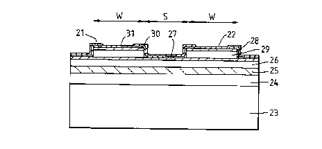
Referring to Figure 3, a specific ultrafast optical
15 switching device is based on a non-linear directional coupler
-20. This comprises two waveguides 21, 22 close enough
together to allow optical coupling between modes propagating
in the guides.
Referring to Figure 3a, in plan view, the directional
20 coupler 20 simply comprlses a device with a pair of parallel
ridge waveguides 21, 22. Referring to Figure 3b, the
construction of these waveguides can be seen in cross
section, being as follows:
(i) A substrate 23 of InP, -lOO~m thick, n-doped;
(ii) A buffer layer 24 of InP, 1.5~m thick and
doped to n = 2 x 10l8;
(iii) An undoped active/waveguide layer 25, of MQW
construction and total thickness 0.4~m;
(iv) A cladding layer 26 of InP, 0.2~m thick and p-
doped to 5 x 10¹⁷;
(v) An etch stop layer 27 of GaInAsP, 0.03~m thick
and p-doped to 5 x 10¹⁷;
(vi) A ridge 28 of each waveguide 21, 22,
comprising InP, l.O~m thick and p-doped to 5 x
10'7;
W094/06054 21 ~ 3 8 1 6 PCT/GB93/01897
- 17 -
(vii) A semiconductor contact layer 29 to each ridge
28, of GaInAs, 0.l~m thick and p-doped to l019;
(viii) An isolator layer 30 of silicon oxide;
(ix) A metal contact layer 31 of Ti/Au.
All doping levels are given in cm~3.
These thicknesses and doping levels quoted are for
illustrative purposes only as a range of different parameters
can give similar device properties.
The two ridges 23 Gf equal width W are separated by a
l0 distance S, formed by etching through the ridge and contact
layers 28, 29 to form channels. The etch stop layer 27 is
used to control the etch depth if a selective chemical
etching process is used.
The active/waveguide layer 25 consists of 32 GaInAs
15 wells, each 65A thick, together with 60A InP barrier layers.
The active/waveguide layer 25 may alternatively have
a more complicated layer structure to separate its two
functions and achieve higher confinement. The well thickness
is chosen to give the desired operating wavelength, while the
20 barrier thickness is chosen to be as thin as possible without
leading to coupling between the carrier bound states in
adjacent wells. The total MQW thickness is then chosen to
give the desired waveguiding properties.
It should be noted that a different number of wells
25 could be used in the active/waveguide layer 24, such as fewer
wells. However, this would affect the coupling length (Lc)
in the device and adjustments might be necessary in the
active~waveguide layer thickness.
The insulating layer 30 is a silicon oxide insulating
30 layer which is windowed above the ridges to allow an ohmic
contact 3l, typically either Ti/Au or Ti/Pt/Au, to be made to
the tops of the waveguides 21, 22. ~Ohmic contact is also
made to the bottom of the substrate 23 before cleaving the
devices to the required length.
Low reflectivity coatings are required on cleaved
facets of the device 20 to minimise any resonant cavity
effects.
wo 94~060s42 1 ~ 3 8 4 6 - 1 ô - PCT/GB93/01897 ~_
The structure described, and shown in Figure 3, gives
a vertical confinement factor of ~ 0.3 for the active
material and single modal operation at 1.55~m for the
individual ridge waveguides 21, 22. At low powers, light
5 launched into one of the guides 21 crosses to the other guide
22 in a distance Lr/ the coupling length, and then back to the
through state, continuing periodically. Coupling lengths for
directional couplers of this type, where the ridges 28 have
a width W of be~ween 2~ and 3~m separated by a gap S of 2~m
10 to 3~m, lie in the range 0.5-4mm. If the waveguides 21, 22
are perturbed then the crossover can be inhibited and the
light remains in the original guide 21.
Referring to Figure 4, as mentioned above, a
demultiplexer can be realised as follows: a high bit rate
15 data stream, consisting of a number of optical TDM channels,
passes through a directional coupler of length Lc and emerges
in the cross state. Applying a high power pulse as a "pump"
at the data rate of a single channel and synchronised with
the desired channel, inhibits crossover for that channel,
20 which therefore emerges in the through state, spatially
separated from the remainder of the bit stream which can also
be recovered if required.
Referring to Figure 5, separation of the switched and
unswitched channels might be done for instance by integration
25 of curved waveguides to achieve a wider spatial separation
(e.g. for optical fibre output), and suitable technology has
already been developed to achieve this, disclosed in
"Integrated Lossless 1 to 4 Optical Splitter/Combiner
Operating at 1.55~m" by D A O Davies, P S Mudhar, M A Fisher,
30 D A H Mace, M J Adams, presented as a post-deadline paper
(PD10) at the ~opical Meeting on Optical Amplifiers and
Applications, Santa Fe, New Mexico, June 24-26 1992.
In Figure 5, two directional couplers 51, 52 are
cascaded. There is an input 53 carrying multiple channels of
35 a high data rate link, and three outputs 54, 55, 56. The
multiple channeis would cross over at each directional
coupler 51, 52 so as to leave the arrangement on the out~ut
2193846
W094/06054 ~ PCT/GB93/01897
-- 19 --
56 furthest spatially (as shown) from the input 53. However,
pumps are used to inhibit crossover at each coupler 51, 52
for a single channel. Thus a single channel is output on
each remaining (and spatially separated) output 54, 55.
The pump and data must be separated to recover the
data at an output and there are a number of approaches that
can be used to achieve this. Codirectional pump and data may
have crossed polarisations or be at different wavelengths,
allowing separation using a polariser or filter respectively.
~~ Tn ei'her case, ~walX-off" of the pulses due to dispersion
and different coupling behaviour needs to be considered.
These effects can be minimised by suitable waveguide design.
Alternatively, contradirectional pump and data could
be used. Here separation at the signal output is not
15 required but the pump pulses need to be longer than the data
pulses, possibly as long as the data pulse transit time in
the device 20, to achieve good overlap in the device 20. The
ability to use the device in pipeline mode twith-more than
one pulse in the device at a time) would then be lost,
20 limiting the multiplexed channel spacing to the device
transit time. This is around lOps for a lmm long device.
This may be acceptable for some applications.
It will be realised that embodiments of the present
invention can provide functional switching, processing or
25 logic devices based on non-linear active waveguides at
transparency. The beneflts of this approach include not only
low optical power requirements, but also compactness, the use
of a mature device processing technology and a clear
potential for integration with other components.
30 Applications could include the non-linear directional coupler
and Mach-Zehnder interferometer referred to above, a Fabry-
- Perot etalon, and grating structures etc. biased at
transparency.
For example, a similar directional coupler to that
35 shown in Figure 3 can be designed to operate as a wavelength
conversion device at very high bit rates. To achieve this a
directional coupler, composed of two parallel amplifiers in
W094/06054 21~ 3 8 ~ 6 PCT/GB93/01897
- 20 -
close proximity and with a common current contact, is
designed to be of length one coupling length over the target
wavelength range of interest. Figure 6 shows two
configurations of such a wavelength converter, Figure 6(a)
5 shows an arrangement having two optical inputs at one input
port, the first being the data signal/ and the second a clock
signal (synchronised with the data signal) at the target
wavelength. The wavelength of the clock may lie anywhere
within the galn spectrum of the amplifier, or over a range of
lO wavelengths below or above this spectrum. The data signal
peak pulse_powers must be sufficient to access the fast non-
linearity at transparency, whilst the clock powers may be
much lower than this. When the clock and signal pulses
coincide, the information will be transferred from the
15 signal wavelength to the clock wavelength and, at the same
time, the resulting information pulse will be emitted from
the appropriate exit port of the device. When this
coincidence does not occur, the clock pulses will be emitted
from the other exit port. The device thus performs the dual
20 function of wavelength conversion and separation of clock and
information outputs. A filter would be required, for the
configuration shown in Figure 6(a), at the output to exclude
wavelengths other than that of the converted data. For a
low-loss (high extinction) device, the requirement for this
25 filter can be relaxed, or for an ideal device dispensed with,
by arranging the clock and signal inputs to be incident at
different input ports; in this case the initial and converted
data are emitted from different exit ports as shown in Figure
6(b).
A further example of a device according to the present
invention comprises laser amplifiers based at transparency in
a non-linear loop mirror (see Figure 7). In this device, the
input (signal) pulse is split in half by coupler CPLR l, with
the half pulses counter-propagating around the loop. In the
35 absence of a pump pulse the signal recombines at CPLR 1 and
no signal emerges from the output port. A strong pump pulse
(at the transparency wavelength for the amplifier bias in
W094/06054 21~ 3 8 ~ 6 PCT/GB93/01897
- 21 -
use) is lntroduced through the wavelength division
multiplexing coupler CPLR 2, and propagates round the loop,
temporally and spatially overlapping the half of the signal
pulse propagating in the same direction. The phase shift
5 introduced in the signai beam co-propagating with the pump
relative to the counter propagating beam will induce
switching when the beams return to the coupler CPLR 1 and
interfere, leading to a non-zero signal at the output.
Applications of such a device could include
LO demultiplexins, as wel, as more general switching in time
division multiplexed systems, optical logic operations and,
since the pump and probe will be at different wavelengths,
wavelength conversion. As for the wavelength converter
comprising a directional coupler, the data signal will need
15 to be at a high power and would, in this example, be launched
into CPLR2, and the clock signal need not be at powers high
enough to access the non-linearity and, in this example,
would be launched into CPLRl. The wavelength converted data
signal would then emerge from CPLRl.
This arrangement is an improvement over known fibre
non-linearity based loop mirrors because the transit time
will be much reduced (a fibre loop mirror can be 10 km long),
and group velocity dispersion will be much less important,
again because the device length will be orders of magnitude
25 less.
The arrangement is also an improvement to previously
published devices where the amplifier is not biased at
transparency, and switching is achieved using long lived
inter-band transitions, for example O'Neill, A.W. and Webb,
30 R.P., "All-optical loop mirror switch employing an asymmetric
amplifier/attenuator combination~, Electronics Lett., 1990,
2~, pp. 2008-2009,-and Eiselt, M., ~Optical loop mirror with
semiconductor laser ampllfer~, Electronics Letts., 1992, 28,
- pp. 1505-1507. Although some devices using the long lived
35 effect such as the SLALOM device (semiconductor laser
amplifier in a loop mirror) described by Eiselt can achieve
switching of data from multi gigabit data streams, the
W094/06054 2~43846 PCT/GB93/01897
- 22 -
relatively long carrier recombination times will cause
patterning unless the pump pulse repetition rate is kept to
below about 1 GHz. In contrast, the device according to the
present invention can respond quasi-instantaneously to pump
5 signals at data rates up to the order of 100 Gbit/s, without
patterning effects, allowing significantly more flexibility
in the application of the device when compared to those
already demonst-ated.
Yet a further example of a device according to the
10 present invention comprises an all-optical clock recovery
device utilising a laser amplifier biased at transparency.
The all-optical recovery of a clock signal from a data stream
using a mode locked laser is known from a paper by Smith &
Lucek, published in Electronics Letts., Vol 28, No.l9, pp.
1814-15, 1992. Here a data stream was used to mode lock a
~fibre laser via a non-linear optical modulator which was
shared between the laser cavity and the transmission fibre.
The non-linear optical modulator comprised a 9 km length of
optical fibre in which the mode locking was achieved by cross
20 phase modulation of the laser light by the data stream.
According to the present invention the length of fibre is
replaced by a semiconductor optical amplifier biased at
transparency which acts as the non-linear optical modulator.
The advantages of this device in terms of reduced size and
25 temperature sensitivity are clear, however most importantly,
because several passes of the cavity are required in order to
achieve mode locking, the reduction in the cavity length
results in greatly reduced delay times before locking occurs.
It is not essential that an embodiment of the present
30 invention has a waveguiding region. Although a waveguiding
region might be used to give a long enough interaction path
for a significant effect to be achieved by use of the optical
pump, alternative structures might for instance incorporate
a resonator arrangement, in which radiation travels to and
35 fro, in order to achieve a suitable lengt~ of interaction
path. Hence, embodiments of the present invention might
W094/06054 21 4 3 ~ 4 6 PCT/GB93/01897
- 23 -
comprise a Fabry-Perot or Confocal arrangement in place of
waveguiding.
In logic devices, there will be one or more signal
(data) inputs. One or more of these might act as the optical
5 pump, there being no need for a separate optical pump input.
The effect of all inputs to the device would be to provide
one or more optical outputs whose level is related to, that
lS determined by, the levels of the inputs. Functions
covered in this way could include:
'~ .hresholding: singlê input beam produces a high output
only when the input level exceeds a
critical value;
'imitlng: output level constrained to be less than
some set value, regardless of input;
5 binary (or higher)
logic operations: multiple inputs giving outputs
determined by the relationships between
signals on different data channels;
bistability: recent history of input signals plays a
part in determining the outputs.
In the above description of specific embodiments of
the present invention, the InP materials system is employed.
This and the AlGaAs~GaAs materials system are currently the
most developed for opto-electronic devices and it is
25 advantageous that the invention could be carried out in
either system. However, it is thought to be the case that
the non-linearity at transparency on which the invention is
based could be observed in any direct bandgap semi-conductor
material.