Note: Descriptions are shown in the official language in which they were submitted.
~O 94/09537 PCT/US93/10000
-1-
The present invention relates to current control circuits for gas discharge
devices, and more particularly to a current control circuit which isolates low
voltage
circuitry from high voltage circuitry.
Gas discharge devices commonly employ a pair of electrodes for passing an
electrical current through the gas within a gas containing cavity and
subsequently
1o initiating a gas discharge. Such gas discharge devices are commonly
employed in
lasers. However, in laser applications, the electrical current passing through
the gas
is commonly controlled so as to establish appropriate characteristics of the
laser
beam. This is particularly important in ring laser gyros as those shown and
described
in U.S. Patent 3,373,650, issued to Killpatrick, and U.S. Patent 3,390,606,
issued to
Podgorski.
In the aforesaid ring laser gyro, commonly employed is a single cathode and a
pair of anodes in which the total electrical current between each pair of
electrodes
must be held constant to within a fraction of a percent to prevent changes in
what is
referred to as the ring laser gyro output bias. Further, not only are the
electrical
2o currents between the cathode and each of the anodes maintained
substantially equal,
but the total current passing into and out of the cathode is held constant
within a
fraction of a percent to prevent changes also in the gyro output bias.
To achieve this goal in ring laser gyros, designers generally build high
voltage
supplies to overcome the large resistance of the gas discharge cavity, and
then the
electrical currents flowing into and out of the cathode is carefully measured
using
sensitive, precision components, and compared to a stable reference current or
voltage. This comparison is then used to create an error signal which is then
fed back
to a high voltage current control circuit which is electrically connected to a
high
voltage electric potential source.
3o In operation, such circuits function so that if the current begins to
deviate
slightly from a desired amount, the error signal that is generated is sent
back to the
current control circuit to compensate, thereby forcing the current to be
regulated.
In such systems it is important to translate the low voltage error signal
provided from a low voltage measuring circuit to the high voltage current
control
circuit. Simple wire connections would allow dangerous high voltages to flow
back
to the low voltage measuring circuits and may subsequently damage them by
exceeding their respective voltage ratings. In the prior art, a common
solution has
i ..
CA 02144414 2002-08-15
'64159-1346
2
been to use several stages of transistors to isolate the
high voltage circuitry from the low voltage measuring
circuits.
SUMMARY OF INVENTION
An object of the present invention is to isolate
the low voltage current measuring circuitry employed in a
gas discharge device from the high voltage current control
circuitry in gas discharge devices and, more particularly,
to ring lasers employed in ring laser gyros.
In the present invention a low voltage comparator
circuit is utilized for comparing the current flowing into
and out of one of the electrodes of a gas discharge device
with a preselected value. In turn, the comparator provides
an output signal to an optical isolation means for
generating light waves in response to the comparator means
output. In turn, the optical isolation means includes a
photosensitive means for providing an output signal which is
responsive to the intensity of light waves generated by the
light generating means. The output of the photosensitive
means in turn is electrically connected to an input means
for a current control which includes a first terminating
means electrically connected to the one electrode of the gas
discharge device, and a second terminating means
electrically connected to the high voltage supply.
In accordance with the present invention there is
provided a current control circuit for a ring laser wherein
said ring laser includes a cathode and two anodes
electrically connected to first and second polarity
terminating means respectively, of a high and a low voltage
electric potential source (+VL, -VH) , respectively, for
passing an electrical current between said cathode and said
i i.
CA 02144414 2002-08-15
'64159-1346
2a
anodes, said current control circuit comprising: isolation
means having, signal input means and signal output means;
current control means having a control signal input means,
and first and second terminating means, said current control
means including a transistor (T200) for controlling the
current passing into and out of said first terminating means
in response to a command signal electrically coupled from
said signal output means to said control signal input means,
wherein said first terminating means is electrically
to connected to said cathode of said ring laser, said second
terminating means is electrically connected to said first
polarity terminating means of said high voltage electrical
potential source; and means for providing to said signal
input means a signal as a function of the difference between
(i) a first signal value representative of current into and
out of said anodes and ( i i ) a second signal value (+Vrei)
representative of a desired current value for said current
into and out of said anodes, characterized in that said
isolation means are optical isolation means comprising: a
light-emitting diode operated between the low voltage
electric potential source (+VL) and said signal input means;
a photo-sensitive transistor adjacent to and responsive to
the intensity of light emitted by said light-emitting diode
and operated between a negative supply voltage (-VH+)
substantially equal to that at the negative said first
polarity terminating means plus an additional positive
voltage value (VP) and said signal output means; and the
emitter of said photo-sensitive transistor being directly
connected to the base of said transistor (T200) of said
current control means via said signal output means and said
control signal input means.
ii
CA 02144414 2002-08-15
'64159-1346
2b
BRIEF DESCRIPTION OF THE DRAWINGS
Figure 1 is a schematic diagram of a current
control circuit of the prior art.
Figure 2 is a current control circuit in
accordance with the present invention.
DETAILED DESCRIPTION OF THE INVENTION
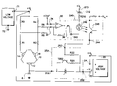
Shown in Figure 1 is a schematic diagram showing a
current control circuit for a ring laser gyro of the prior
art. Thereshown is a gas discharge device 10 in the form of
a ring laser gyro as particularly described in U.S. Patent
3,373,650, issued to Killpatrick, and U.S. Patent 3,390,606,
issued to Podgorski. As is well understood in the ring
laser gyro art, a block is provided for containing a gas. A
plurality of electrodes are in communication with the gas in
order to pass a discharge current therethrough and
subsequently produce a pair of counter-propagating laser
beams travelling along an optical closed-loop path.
Referring particularly now to the drawing of Figure 1, the
gas discharge device includes a first electrode 12
electrically connected to the negative polarity terminating
means 22 of high voltage electric potential source 20.
Further, a gas discharge device 10 includes a second
electrode 14 electrically connected to the positive polarity
terminating means 24 of high voltage electric potential
source 20 through series resistors R1 and R2. Similarly,
electrode
~O 94/09537 PCT/US93/10000
-3- 214~~~.
16 is electrically connected to the positive polarity terminating means 24 of
high
voltage electrical potential source 20 through resistors R3 and R4. By virtue
of the
electrical connection of electrodes 14 and 16 to the positive polarity
terminating
means 24, electrodes 14 and 16 become the anodes of gas discharge device 10,
and
electrode 12 is the cathode.
Also illustrated in Figure 1 is a low voltage power supply 70 having a
positive
low voltage output, designated 71, and also as +VL, and a negative low voltage
output 72 connected to circuit ground. The positive low voltage output 71 is
1o electrically connected to the junction of resistors R2 and R4 as well as
other circuit
components, for example operational amplifier 30 (not shown) to provide low
voltage
circuit power. Also, the positive polarity output 71 is also electrically
connected to
the positive polarity terminating means 24 in order to provide a complete
electrical
control circuit.
The junction of resistors R1 and R2 is electrically connected to an input
means
32 of a comparator means 30 through resistor R5. The junction of resistors R3
and
R4 is also electrically connected to input means 32 through resistor R6.
Comparator
means 30 is schematically shown as a summing amplifier having the negative
input
2o thereof being input means 32, and the positive input thereof being
electrically
connected to an electric potential designated as Vref. Comparator means 30
includes
output means 36 which is proportional the voltage difference between input
means 34
and 32.
The comparator 30 output means 36 is electrically connected to input means
52 of current control circuit 50 through an electrical isolation circuit 40
including
input terminating means 42 and output terminating means 44. Electrical
isolation
circuit 40 includes a pair of transistors Tl and T2 connected in series, and
resistors
R7, R8, R9, R10 and Rll. Zener diode 43, and resistors R7 and R8 form a
biasing
arrangement for transistors Tl and T2. Resistors R9, R10 and Rll are generally
high
3o resistance values in the megohm range. As will more fully be described,
electrical
isolation circuit 40 essentially isolates the low voltage circuit at the
output 36 of
comparator 30 from the high voltage current control circuit 50.
Current control circuit 50 includes a transistor T3 having collector thereof
electrically connected to electrode 12, and the emitter thereof electrically
connected to
negative polarity terminating means 22 through limiting resistor R12. Current
control
circuit SO also includes a transistor biasing arrangement and isolation
circuit including
diodes 61, 62 and 63 and resistors R13 and R14.
WO 94/09537 PCT/US93/1001~
.. t f K' ~~ ~4 . -L~._
The circuit operation of Figure 1 will now briefly be described. The input
signal electrically connected to the input means 32 of comparator means 32
represents
the total electrical current passing into and out of electrode 12. In turn,
the output
means 36 of comparator 30 provides a command signal representative of the
difference in voltages between input means 32 and 34 as aforesaid. In turn,
the
command signal is electrically connected to input means 52 of current control
circuit
50 through the electrical isolation circuit 40 for controlling the current
passing
through transistor T3 and into and out of current control circuit terminating
means 54.
In closed-loop operation, as should be well understood to those skilled in the
art, the
to combination of comparator means 30 and current control circuit 50 serve to
maintain
a constant electrical current passing into and out of electrode 12.
As indicated earlier, fault tolerant system designs require isolation of
failures
as an aspect of their architecture. A transistor level shifter, like those
shown in the
isolation circuit 40, have a failure mode in which the transistors may short,
allowing
high voltage to pass through them. In turn, this may cause catastrophic
failure to low
voltage circuits and other circuits common to an electrical board, which in
turn may
cause catastrophic failure to the entire system. In the present invention, an
optical
isolation technique is employed to avoid a potential for catastrophic failure
due to
transistor short-circuits.
2o Shown in Figure 2 is essentially the circuit of Figure 1 with the
electrical
isolation circuit 40 replaced by electrical isolation circuit 240, and the
current control
circuit 50 replaced by current control circuit 250. In Figure 2, thereshown
are circuit
components of Figure 1 with similarly functioning and arranged circuit
components in
Figure 2 having the same numeral designations as in the previously described
Figure.
Now referring more particularly to Figure 2, thereshown is an optical
isolation
means 240 having a signal input means 242 and a signal output means 244.
Optical
isolation means includes a light generating means illustrated as a light
emitting diode
246 for producing light waves having an intensity in response to a command
signal
electrically coupled to the signal input means 242. Further, optical isolation
means
240 also includes a photosensitive means illustrated as a photosensitive
transistor 248
having the emitter thereof electrically connected to signal output means 244.
Optical isolation means 240 further includes a current biasing arrangement
including a current supply means illustrated as and including a supply voltage
VL
connected to terminating means 210 and also zener diode 212 in series with
resistor ,
8200.
The collector of photosensitive transistor 248 is electrically connected to a
negative supply voltage substantially equal to that at the negative polarity
terminating
means 22 plus an additional positive voltage value Vp, e.g., +20 volts.
~O 94/09537 PCT/US93/10000
-s- 2~.~~.~
Current control means 250 includes control transistor T200 having the
collector thereof connected to a first output terminating means 254, which in
turn is
electrically connected to electrode 12. The emitter of transistor T200 is
electrically
connected to the negative polarity terminating means 22 through current
limiting
resistor R20 and second output terminating means 256. Transistor T200 further
includes a biasing resistor R22 between the base of transistor T200 and output
terminating means 256.
The circuit operation of Figure 2 in accordance with the present invention
will
no be described. As before, the output terminating means 36 of comparator 30
1o provides an output signal representative of the difference in voltage
between voltage
signals at the inputs 32 and 34. The output terminating means 36 being
electrically
connected to the input means 242 of optical isolation means 240 substantially
controls
the current passing through the light emitting diode 246. In turn, transistor
248
provides an electrical current into and out of terminating means 244 which is
a
i5 function of the light intensity generated by the light emitting diode 246.
In turn, by virtue of output means 244 of optical isolation means 240 being
electrically connected to the current control input means 252, the current
passing
through transistor T200 is regulated in response to the current into and out
of input
means 252.
2o Therefore, the circuit of Figure 2 functions in a similar manner to Figure
1 for
maintaining the current passing into and out of electrode 12 to a constant
value as
determined by the reference voltage provided at the input means 34 of
comparator
means 30. However, by virtue of the optical isolation means 240, the high
voltage
circuit is electrically isolated from the low voltage circuit. This in turn
provides a
2s circuit which obviates the catastrophic breakdown of a transistor short due
to high
voltages as was the case in the prior art with use of the transistor isolation
circuit 40
of Figure 1.
Those skilled in the art will recognize that only a preferred embodiment of
the
present invention has been disclosed herein and that the embodiments thereof
may be
3o altered and modified without departing from the true spirit and scope of
the invention
as defined in the accompanying Claims.
More specifically, although the circuit is particularly applicable to ring
laser
gyros, the circuit is also applicable to any gas discharge device in which it
is intended
to isolate the low voltage from the high voltage circuits which power the gas
35 discharge device. Further, there are a wide variety of packaged, so called,
"opto-
isolator" circuits for providing optical isolation means 240, and are all
intended to be
within the scope of the present invention and accompanying claims.